EP3640975B1 - Dispositif et procédé de liaison de substrats - Google Patents
Dispositif et procédé de liaison de substrats Download PDFInfo
- Publication number
- EP3640975B1 EP3640975B1 EP19215305.4A EP19215305A EP3640975B1 EP 3640975 B1 EP3640975 B1 EP 3640975B1 EP 19215305 A EP19215305 A EP 19215305A EP 3640975 B1 EP3640975 B1 EP 3640975B1
- Authority
- EP
- European Patent Office
- Prior art keywords
- plate
- substrate
- mounting device
- curvature
- substrates
- Prior art date
- Legal status (The legal status is an assumption and is not a legal conclusion. Google has not performed a legal analysis and makes no representation as to the accuracy of the status listed.)
- Active
Links
Images
Classifications
-
- H—ELECTRICITY
- H10—SEMICONDUCTOR DEVICES; ELECTRIC SOLID-STATE DEVICES NOT OTHERWISE PROVIDED FOR
- H10W—GENERIC PACKAGES, INTERCONNECTIONS, CONNECTORS OR OTHER CONSTRUCTIONAL DETAILS OF DEVICES COVERED BY CLASS H10
- H10W95/00—Packaging processes not covered by the other groups of this subclass
-
- H—ELECTRICITY
- H10—SEMICONDUCTOR DEVICES; ELECTRIC SOLID-STATE DEVICES NOT OTHERWISE PROVIDED FOR
- H10P—GENERIC PROCESSES OR APPARATUS FOR THE MANUFACTURE OR TREATMENT OF DEVICES COVERED BY CLASS H10
- H10P10/00—Bonding of wafers, substrates or parts of devices
- H10P10/12—Bonding of semiconductor wafers or semiconductor substrates to semiconductor wafers or semiconductor substrates
- H10P10/128—Bonding of semiconductor wafers or semiconductor substrates to semiconductor wafers or semiconductor substrates by direct semiconductor to semiconductor bonding
-
- H—ELECTRICITY
- H10—SEMICONDUCTOR DEVICES; ELECTRIC SOLID-STATE DEVICES NOT OTHERWISE PROVIDED FOR
- H10P—GENERIC PROCESSES OR APPARATUS FOR THE MANUFACTURE OR TREATMENT OF DEVICES COVERED BY CLASS H10
- H10P72/00—Handling or holding of wafers, substrates or devices during manufacture or treatment thereof
- H10P72/04—Apparatus for manufacture or treatment
- H10P72/0428—Apparatus for mechanical treatment or grinding or cutting
-
- H—ELECTRICITY
- H10—SEMICONDUCTOR DEVICES; ELECTRIC SOLID-STATE DEVICES NOT OTHERWISE PROVIDED FOR
- H10P—GENERIC PROCESSES OR APPARATUS FOR THE MANUFACTURE OR TREATMENT OF DEVICES COVERED BY CLASS H10
- H10P72/00—Handling or holding of wafers, substrates or devices during manufacture or treatment thereof
- H10P72/04—Apparatus for manufacture or treatment
- H10P72/0438—Apparatus for making assemblies not otherwise provided for, e.g. package constructions
-
- H—ELECTRICITY
- H10—SEMICONDUCTOR DEVICES; ELECTRIC SOLID-STATE DEVICES NOT OTHERWISE PROVIDED FOR
- H10P—GENERIC PROCESSES OR APPARATUS FOR THE MANUFACTURE OR TREATMENT OF DEVICES COVERED BY CLASS H10
- H10P72/00—Handling or holding of wafers, substrates or devices during manufacture or treatment thereof
- H10P72/06—Apparatus for monitoring, sorting, marking, testing or measuring
- H10P72/0616—Monitoring of warpages, curvatures, damages, defects or the like
-
- H—ELECTRICITY
- H10—SEMICONDUCTOR DEVICES; ELECTRIC SOLID-STATE DEVICES NOT OTHERWISE PROVIDED FOR
- H10P—GENERIC PROCESSES OR APPARATUS FOR THE MANUFACTURE OR TREATMENT OF DEVICES COVERED BY CLASS H10
- H10P72/00—Handling or holding of wafers, substrates or devices during manufacture or treatment thereof
- H10P72/70—Handling or holding of wafers, substrates or devices during manufacture or treatment thereof for supporting or gripping
- H10P72/72—Handling or holding of wafers, substrates or devices during manufacture or treatment thereof for supporting or gripping using electrostatic chucks
- H10P72/722—Details of electrostatic chucks
-
- H—ELECTRICITY
- H10—SEMICONDUCTOR DEVICES; ELECTRIC SOLID-STATE DEVICES NOT OTHERWISE PROVIDED FOR
- H10P—GENERIC PROCESSES OR APPARATUS FOR THE MANUFACTURE OR TREATMENT OF DEVICES COVERED BY CLASS H10
- H10P72/00—Handling or holding of wafers, substrates or devices during manufacture or treatment thereof
- H10P72/70—Handling or holding of wafers, substrates or devices during manufacture or treatment thereof for supporting or gripping
- H10P72/76—Handling or holding of wafers, substrates or devices during manufacture or treatment thereof for supporting or gripping using mechanical means, e.g. clamps or pinches
-
- H—ELECTRICITY
- H10—SEMICONDUCTOR DEVICES; ELECTRIC SOLID-STATE DEVICES NOT OTHERWISE PROVIDED FOR
- H10P—GENERIC PROCESSES OR APPARATUS FOR THE MANUFACTURE OR TREATMENT OF DEVICES COVERED BY CLASS H10
- H10P72/00—Handling or holding of wafers, substrates or devices during manufacture or treatment thereof
- H10P72/70—Handling or holding of wafers, substrates or devices during manufacture or treatment thereof for supporting or gripping
- H10P72/76—Handling or holding of wafers, substrates or devices during manufacture or treatment thereof for supporting or gripping using mechanical means, e.g. clamps or pinches
- H10P72/7604—Handling or holding of wafers, substrates or devices during manufacture or treatment thereof for supporting or gripping using mechanical means, e.g. clamps or pinches the wafers being placed on a susceptor, stage or support
- H10P72/7611—Handling or holding of wafers, substrates or devices during manufacture or treatment thereof for supporting or gripping using mechanical means, e.g. clamps or pinches the wafers being placed on a susceptor, stage or support characterised by edge profile or support profile
-
- H—ELECTRICITY
- H10—SEMICONDUCTOR DEVICES; ELECTRIC SOLID-STATE DEVICES NOT OTHERWISE PROVIDED FOR
- H10P—GENERIC PROCESSES OR APPARATUS FOR THE MANUFACTURE OR TREATMENT OF DEVICES COVERED BY CLASS H10
- H10P72/00—Handling or holding of wafers, substrates or devices during manufacture or treatment thereof
- H10P72/70—Handling or holding of wafers, substrates or devices during manufacture or treatment thereof for supporting or gripping
- H10P72/78—Handling or holding of wafers, substrates or devices during manufacture or treatment thereof for supporting or gripping using vacuum or suction, e.g. Bernoulli chucks
-
- H—ELECTRICITY
- H10—SEMICONDUCTOR DEVICES; ELECTRIC SOLID-STATE DEVICES NOT OTHERWISE PROVIDED FOR
- H10P—GENERIC PROCESSES OR APPARATUS FOR THE MANUFACTURE OR TREATMENT OF DEVICES COVERED BY CLASS H10
- H10P90/00—Preparation of wafers not covered by a single main group of this subclass, e.g. wafer reinforcement
- H10P90/19—Preparing inhomogeneous wafers
- H10P90/1904—Preparing vertically inhomogeneous wafers
- H10P90/1906—Preparing SOI wafers
- H10P90/1914—Preparing SOI wafers using bonding
-
- H—ELECTRICITY
- H10—SEMICONDUCTOR DEVICES; ELECTRIC SOLID-STATE DEVICES NOT OTHERWISE PROVIDED FOR
- H10W—GENERIC PACKAGES, INTERCONNECTIONS, CONNECTORS OR OTHER CONSTRUCTIONAL DETAILS OF DEVICES COVERED BY CLASS H10
- H10W10/00—Isolation regions in semiconductor bodies between components of integrated devices
- H10W10/10—Isolation regions comprising dielectric materials
- H10W10/181—Semiconductor-on-insulator [SOI] isolation regions, e.g. buried oxide regions of SOI wafers
-
- H—ELECTRICITY
- H10—SEMICONDUCTOR DEVICES; ELECTRIC SOLID-STATE DEVICES NOT OTHERWISE PROVIDED FOR
- H10W—GENERIC PACKAGES, INTERCONNECTIONS, CONNECTORS OR OTHER CONSTRUCTIONAL DETAILS OF DEVICES COVERED BY CLASS H10
- H10W72/00—Interconnections or connectors in packages
- H10W72/071—Connecting or disconnecting
- H10W72/0711—Apparatus therefor
-
- H—ELECTRICITY
- H10—SEMICONDUCTOR DEVICES; ELECTRIC SOLID-STATE DEVICES NOT OTHERWISE PROVIDED FOR
- H10W—GENERIC PACKAGES, INTERCONNECTIONS, CONNECTORS OR OTHER CONSTRUCTIONAL DETAILS OF DEVICES COVERED BY CLASS H10
- H10W72/00—Interconnections or connectors in packages
- H10W72/90—Bond pads, in general
-
- H—ELECTRICITY
- H10—SEMICONDUCTOR DEVICES; ELECTRIC SOLID-STATE DEVICES NOT OTHERWISE PROVIDED FOR
- H10W—GENERIC PACKAGES, INTERCONNECTIONS, CONNECTORS OR OTHER CONSTRUCTIONAL DETAILS OF DEVICES COVERED BY CLASS H10
- H10W99/00—Subject matter not provided for in other groups of this subclass
-
- H—ELECTRICITY
- H10—SEMICONDUCTOR DEVICES; ELECTRIC SOLID-STATE DEVICES NOT OTHERWISE PROVIDED FOR
- H10W—GENERIC PACKAGES, INTERCONNECTIONS, CONNECTORS OR OTHER CONSTRUCTIONAL DETAILS OF DEVICES COVERED BY CLASS H10
- H10W72/00—Interconnections or connectors in packages
- H10W72/01—Manufacture or treatment
- H10W72/0198—Manufacture or treatment batch processes
-
- H—ELECTRICITY
- H10—SEMICONDUCTOR DEVICES; ELECTRIC SOLID-STATE DEVICES NOT OTHERWISE PROVIDED FOR
- H10W—GENERIC PACKAGES, INTERCONNECTIONS, CONNECTORS OR OTHER CONSTRUCTIONAL DETAILS OF DEVICES COVERED BY CLASS H10
- H10W72/00—Interconnections or connectors in packages
- H10W72/071—Connecting or disconnecting
-
- H—ELECTRICITY
- H10—SEMICONDUCTOR DEVICES; ELECTRIC SOLID-STATE DEVICES NOT OTHERWISE PROVIDED FOR
- H10W—GENERIC PACKAGES, INTERCONNECTIONS, CONNECTORS OR OTHER CONSTRUCTIONAL DETAILS OF DEVICES COVERED BY CLASS H10
- H10W72/00—Interconnections or connectors in packages
- H10W72/071—Connecting or disconnecting
- H10W72/0711—Apparatus therefor
- H10W72/07163—Means for mechanical processing, e.g. for planarising, pressing, stamping or drilling
-
- H—ELECTRICITY
- H10—SEMICONDUCTOR DEVICES; ELECTRIC SOLID-STATE DEVICES NOT OTHERWISE PROVIDED FOR
- H10W—GENERIC PACKAGES, INTERCONNECTIONS, CONNECTORS OR OTHER CONSTRUCTIONAL DETAILS OF DEVICES COVERED BY CLASS H10
- H10W72/00—Interconnections or connectors in packages
- H10W72/071—Connecting or disconnecting
- H10W72/0711—Apparatus therefor
- H10W72/07178—Means for aligning
-
- H—ELECTRICITY
- H10—SEMICONDUCTOR DEVICES; ELECTRIC SOLID-STATE DEVICES NOT OTHERWISE PROVIDED FOR
- H10W—GENERIC PACKAGES, INTERCONNECTIONS, CONNECTORS OR OTHER CONSTRUCTIONAL DETAILS OF DEVICES COVERED BY CLASS H10
- H10W72/00—Interconnections or connectors in packages
- H10W72/071—Connecting or disconnecting
- H10W72/0711—Apparatus therefor
- H10W72/07183—Means for monitoring
-
- H—ELECTRICITY
- H10—SEMICONDUCTOR DEVICES; ELECTRIC SOLID-STATE DEVICES NOT OTHERWISE PROVIDED FOR
- H10W—GENERIC PACKAGES, INTERCONNECTIONS, CONNECTORS OR OTHER CONSTRUCTIONAL DETAILS OF DEVICES COVERED BY CLASS H10
- H10W72/00—Interconnections or connectors in packages
- H10W72/071—Connecting or disconnecting
- H10W72/073—Connecting or disconnecting of die-attach connectors
- H10W72/07331—Connecting techniques
-
- H—ELECTRICITY
- H10—SEMICONDUCTOR DEVICES; ELECTRIC SOLID-STATE DEVICES NOT OTHERWISE PROVIDED FOR
- H10W—GENERIC PACKAGES, INTERCONNECTIONS, CONNECTORS OR OTHER CONSTRUCTIONAL DETAILS OF DEVICES COVERED BY CLASS H10
- H10W72/00—Interconnections or connectors in packages
- H10W72/071—Connecting or disconnecting
- H10W72/073—Connecting or disconnecting of die-attach connectors
- H10W72/07331—Connecting techniques
- H10W72/07332—Compression bonding, e.g. thermocompression bonding
-
- H—ELECTRICITY
- H10—SEMICONDUCTOR DEVICES; ELECTRIC SOLID-STATE DEVICES NOT OTHERWISE PROVIDED FOR
- H10W—GENERIC PACKAGES, INTERCONNECTIONS, CONNECTORS OR OTHER CONSTRUCTIONAL DETAILS OF DEVICES COVERED BY CLASS H10
- H10W80/00—Direct bonding of chips, wafers or substrates
- H10W80/011—Manufacture or treatment of pads or other interconnections to be direct bonded
- H10W80/031—Changing or setting shapes of the pads
- H10W80/037—Changing or setting shapes of the pads by mechanical treatment, e.g. by cutting, pressing or stamping
-
- H—ELECTRICITY
- H10—SEMICONDUCTOR DEVICES; ELECTRIC SOLID-STATE DEVICES NOT OTHERWISE PROVIDED FOR
- H10W—GENERIC PACKAGES, INTERCONNECTIONS, CONNECTORS OR OTHER CONSTRUCTIONAL DETAILS OF DEVICES COVERED BY CLASS H10
- H10W80/00—Direct bonding of chips, wafers or substrates
- H10W80/161—Aligning
- H10W80/163—Aligning using active alignment, e.g. detecting marks and correcting position
-
- H—ELECTRICITY
- H10—SEMICONDUCTOR DEVICES; ELECTRIC SOLID-STATE DEVICES NOT OTHERWISE PROVIDED FOR
- H10W—GENERIC PACKAGES, INTERCONNECTIONS, CONNECTORS OR OTHER CONSTRUCTIONAL DETAILS OF DEVICES COVERED BY CLASS H10
- H10W90/00—Package configurations
- H10W90/701—Package configurations characterised by the relative positions of pads or connectors relative to package parts
- H10W90/791—Package configurations characterised by the relative positions of pads or connectors relative to package parts of direct-bonded pads
- H10W90/792—Package configurations characterised by the relative positions of pads or connectors relative to package parts of direct-bonded pads between multiple chips
Definitions
- the present invention relates to a method for bonding a first substrate to a second substrate, a corresponding device and a plate according to the independent claims.
- JP2009010072A discloses a substrate bonding device having a substrate holding part, a support body holding part aligned with the substrate holding part and provided on the substrate holding part in a contactable or detachable manner with a suction holder of a support body 50.
- Chucks are available in a wide variety of designs.
- the decisive factor for the chuck is a flat receiving surface or mounting surface for holding/fixing the substrates so that the structures on the substrates can be correctly aligned and contacted over the entire substrate surface.
- US20120077329A1 describes a method to obtain a desired alignment accuracy between the functional units of two substrates during and after bonding by not fixing the lower substrate.
- the lower substrate is not subject to any boundary conditions and can bond freely to the upper substrate during the bonding process.
- the alignment process plays a key role in bonding substrates.
- One of the biggest technical problems when bonding two substrates is the alignment accuracy of the functional units between the individual substrates.
- the substrates can be aligned very precisely with each other using alignment equipment, distortions of the substrates can also occur during the bonding process. Due to the distortions that occur during the bonding process, the functional units are not necessarily correctly aligned with each other at all positions.
- the alignment inaccuracy at a certain point on the substrate can be a result of distortion, a scaling error, a lens error (magnification or reduction error), etc.
- Overlay refers to the coverage accuracy of structures from different manufacturing steps.
- Overlay errors are referred to as "run-out” errors, which are primarily caused by a distortion of at least one substrate during a bonding process.
- the distortion of at least one substrate also distorts the functional units of the first substrate in relation to the functional units of the second substrate.
- the resulting "run-out" errors are radially symmetrical around the contact point, and therefore increase from the contact point to the circumference. In most cases, the increase in the run-out errors is linear. Under special conditions, however, the run-out errors can also increase non-linearly.
- the object of the present invention is to provide a device and a method for bonding two substrates, with which the bonding accuracy is increased.
- the invention is based on the idea that a plate is arranged between at least one of the substrates and the corresponding receiving device, wherein the substrate with the plate is curved relative to the receiving device before and/or during bonding.
- a preferably flat receiving surface of the receiving device for receiving the plate and the substrate is therefore not deformed in particular.
- the receiving device serves to deform/curve the plate, wherein the substrate fixed to the plate is also curved by the curvature of the plate.
- the invention describes in particular a method and a device for improved bonding of two substrates. In particular, this means minimizing the "run-out" error.
- the invention is based in particular on the idea of placing a plate between the substrate and the receiving device, which can be fixed by the receiving device on the one hand and is itself able to fix the substrate.
- the plate preferably a ceramic plate, is fixed in particular by a receiving device that is able to control the fixation locally.
- the fixations (in particular consisting of fixing means/fixing elements) are grouped in particular in several zones.
- Preferably in the center of the receiving device there is a device for bending the plate, in particular only partially fixed.
- the bending device is referred to as a curvature element.
- the curvature element is in particular a nozzle through which a fluid, preferably a gas, can exit in order to generate an overpressure between the plate and the receiving device, which curves the plate and thus the substrate fixed to the plate.
- a fluid preferably a gas
- the plate is curved.
- the plate preferably holds the substrate fixed during the bonding process and thus creates a system consisting of the plate and the substrate.
- the system and/or the plate have a higher bending resistance than the substrate alone.
- the increased bending resistance of this system has a positive effect on minimizing the run-out error.
- the bending resistance is characterized by the bending resistance moment.
- a core of the invention consists in particular in positioning a plate between at least one of the two substrates and the receiving device, which plate can be curved.
- the plate is curved, in particular in the center or from the center of the substrate or plate, using a curvature mechanism, in particular using compressed air. Since the bending of the two substrates takes place at a certain distance, the gap is preferably reduced as the bonding wave advances in order to enable full-surface contact of the substrates.
- a curvature element of the curvature mechanism for effecting the curvature is arranged in particular within the fixation, preferably in the center.
- the fixation, in particular the holding vacuum, of the holding device is deactivated, while the curvature mechanism, in particular the compressed air, remains activated.
- the lower plate thus floats on an air cushion in this state, provided compressed air is used, and enables full-surface contact of the substrates.
- the plate fixes the substrate, increasing its thickness and thus its flexural rigidity. In particular, its flexibility is also reduced, so that the bonding result is significantly improved.
- the fixation of the substrate by the plate or on the plate, in particular the vacuum is preferably maintained via a fixing element connection, which is in particular stretchable or extendible.
- the fixation of the substrate on the plate can thus be independent of the Control and fixation of the plate to the receiving device must be maintained.
- a significant advantage of the invention is therefore that different errors, in particular the "run-out” error and the residual errors, can be almost completely eliminated.
- Translation and/or rotation errors are mainly due to an inaccurate alignment of the two substrates to each other before the bonding process begins. Therefore, the alignment of the substrates is carried out as best as possible, preferably with appropriate alignment devices.
- Example alignment devices are described in the publications US6214692B1 , WO2014202106A1 , WO2015082020A1 described, to which particular reference is made.
- the alignment is preferably carried out using alignment marks and/or using the functional units present on the substrates.
- the alignment accuracy is in particular better than 500 nm, preferably better than 300 nm, even more preferably better than 150 nm, most preferably better than 100 nm, most preferably better than 20 nm.
- the run-out error between two structures is in particular smaller than 500 nm, preferably smaller than 300 nm, even more preferably smaller than 150 nm, most preferably smaller than 100 nm, most preferably smaller than 20 nm.
- the residual errors are in particular smaller than 100 nm, preferably smaller than 50, even more preferably smaller than 30 nm, most preferably smaller than 20 nm, most preferably smaller than 10 nm.
- the overlay can be reduced to less than 500 nm, preferably less than 300 nm, even more preferably less than 150 nm, most preferably less than 100 nm, most preferably less than 50 nm.
- the device according to the invention is able to carry out an optimal bonding process with the help of control loops.
- the flexibility can be specifically adjusted, especially by adjusting the bending stiffness.
- several such plates can exist, which can be exchanged in the simplest way, quickly, efficiently and inexpensively. This means that adaptation to the respective substrate is possible at any time, especially when using different substrates.
- the invention is based on the idea that at least one of the two substrates, preferably both substrates, are deformed to align the contact surfaces, in particular before and/or during bonding, preferably during fusion bonding, and that a plate is arranged between at least one of the two substrates and the receiving device, on which the substrate is fixed while the plate itself is fixed to the receiving device.
- Deformation refers in particular to a state that deviates from the initial state, in particular the initial geometry, of the substrates.
- the invention thus relates to a method and a device for reducing or completely avoiding the "run-out" error between two bonded substrates, in particular by means of thermodynamic and/or mechanical compensation mechanisms, during bonding. Furthermore, the invention relates to a corresponding article which is produced using the device and the method according to the invention.
- bonding is initiated after contacting the contact surfaces of the substrates, in particular by detaching the upper and/or lower plates.
- the use of at least one plate according to the invention also enables very precisely controlled detachment, since the stiffening of the substrate by the plate increases the bending resistance of the system consisting of substrate and plate.
- methods for bonding are therefore also described in the further course of the document which are based on a targeted and controlled bonding process, which can dispense with spontaneous dropping of the upper substrate and/or the upper plate with the substrate fixed to it.
- the embodiment according to the invention is first described using a receiving device with a plate and a substrate.
- a device is also later disclosed which has two such receiving devices. It may be that the plate according to the invention is used only on one of the two receiving devices or on both receiving devices. If only one plate is used, it can be located on the upper, but preferably on the lower receiving device.
- the most preferred embodiment according to the invention consists in two to use plates according to the invention, one each between a substrate and the associated receiving device.
- the first and/or second substrate is preferably radially symmetrical.
- the substrate can have any diameter, the substrate diameter is in particular 1 inch, 2 inches, 3 inches, 4 inches, 5 inches, 6 inches, 8 inches, 12 inches, 18 inches or greater than 18 inches.
- the thickness of the first and/or second substrate is between 1 ⁇ m and 2000 ⁇ m, preferably between 10 ⁇ m and 1500 ⁇ m, more preferably between 100 ⁇ m and 1000 ⁇ m.
- a substrate can also have a rectangular shape or at least a shape deviating from the circular shape.
- a substrate is understood to mean in particular a wafer.
- the substrates have approximately identical diameters D1 and D2, which differ from each other in particular by less than 5 mm, preferably less than 3 mm, even more preferably less than 1 mm.
- a further, particularly independent, aspect is the design of the plate and its use between the substrate and the receiving device.
- the plate is arranged with its side facing away from the substrate on a curvature means or a curvature-changing means of the receiving device.
- the substrate is thus not deformed directly, but the deformation of the substrate takes place indirectly through the deformation of the plate by the curvature-changing means.
- the plate is preferably fixed/fixable to the receiving device.
- the plate is in particular made predominantly, preferably entirely, from a ceramic, preferably a technical ceramic.
- the plate can be coated.
- the plate has the same diameter as the substrate fixed/fixable on it.
- the plate has a larger radius than the substrate to be fixed to it. Since the plate has a larger diameter than the substrate, the plate can be fixed to the receiving device in an advantageous manner, in particular exclusively, in the area projecting beyond the substrate.
- the radius of the plate corresponds to at least 1.01 times, preferably more than 1.1 times, even more preferably more than 1.2 times, most preferably more than 1.3 times, most preferably more than 1.4 times, the radius of the substrate to be fixed.
- Particularly preferred embodiments of the plate according to the invention have diameters that are between 10% and 20% larger than the diameters of the substrates to be fixed.
- a thin substrate has a very low bending resistance due to its small thickness.
- the low bending resistance leads to an extremely high flexibility, which makes it difficult to control the bonding process in a targeted manner.
- This has the disadvantage that defects in the center, especially gas bubbles (voids), can have a negative impact on the bonding result.
- the additional By supporting the substrates with the plate, the low bending resistance of the substrate becomes irrelevant, since the plate supports the substrate fixed to it during the bonding process.
- a particularly independent aspect of the invention consists in forming a system from the plate and a substrate which has a higher bending resistance than the individual substrate (without plate).
- the plate can have steps, particularly at the edge.
- the steps are removed in particular in the direction of the receiving device, so that there is a peripheral empty space between the plate and the receiving device. This empty space allows for more optimal deformation of the plate in the edge area and thus supports the deformation.
- the plate according to the invention can be supported and fixed on several piezo elements. This measure allows the plate to be deformed locally.
- the plate is characterized by material parameters such as purity, inherent rigidity, flatness and deformability.
- the plate lies between the support device and the substrate fixed/fixable to it. On the one hand, it will be thick enough not to be deformed by unwanted external influences and to be able to provide sufficient support for the substrate lying on it, and on the other hand, it will be thin enough to be bent by a targeted force (compressed air, vacuum, mechanical, pneumatic or electrical actuator).
- the plate can be made into a convex and/or concave shape.
- the plate has a heat resistance of more than 500°C, preferably more than 750°C, more preferably more than 1000°C.
- the plate is a ceramic plate.
- the plate is made of a special oxide ceramic, in particular aluminum oxide Al 2 O 3 .
- the plate consists of a high-strength, elastically deformable membrane.
- the elastic membrane can consist of a film material.
- a radius of curvature of the first and/or second plate during bonding, in particular at the start of bonding is in particular greater than 0.01 m, preferably greater than 0.1 m, more preferably greater than 1 m, even more preferably greater than 10 m, most preferably greater than 100 m, most preferably greater than 1000 m.
- the radius of curvature of the first/lower plate is the same as the radius of curvature of the second/upper plate. This results in a starting position for bonding that is symmetrical in terms of geometry.
- the radius of curvature of the plate is adjustable. Due to the controlled curvature of the plates, it is preferred according to the invention if the radius of curvature of both substrates, in particular at the bond front, differs from one another by less than 5%, and is even more preferably the same.
- the thickness of the deformable plate is in particular between 0.1 and 10 mm, preferably between 0.25 and 8 mm, more preferably between 0.5 and 6 mm, most preferably between 1 and 5 mm.
- the elastic modulus is a material property that describes the relationship between strain and stress during the deformation of a solid body with linear elastic behavior.
- the E-modulus of the plate is between 0.01 GPa and 1100 GPa, preferably between 0.1 GPa and 800 GPa, even more preferably between 1 GPa and 600 GPa, most preferably between 10 GPa and 500 GPa, most preferably between 100 GPa and 450 GPa.
- the plate has a higher modulus of elasticity than the substrate.
- the plate has sufficient inherent rigidity to ensure easy handling and to provide optimal support properties for the substrates.
- the roughness of the plate is specified either as mean roughness, root mean square roughness or as average roughness depth.
- the determined values for mean roughness, root mean square roughness and average roughness depth generally differ for the same measuring section or measuring surface, but are in the same order of magnitude. Therefore, the following numerical value ranges for the roughness are to be understood either as values for mean roughness, root mean square roughness or for the average roughness depth.
- the roughness is less than 100 ⁇ m, preferably less than 10 ⁇ m, even more preferably less than 1 ⁇ m, most preferably less than 100 nm, most preferably less than 10 nm.
- a further idea according to the invention which is particularly independent or can be combined with the aforementioned, consists in the use of a deformation element as a curvature means and/or curvature changing means.
- the plates and/or the substrates are curved.
- the curvature is the reciprocal of the radius of curvature of a circle (two-dimensional) or a sphere (three-dimensional) at the ossification point at which the curvature is to be determined.
- the curvature of a plate and/or a substrate can therefore be position-dependent in particular.
- the curvature is constant for all points on a circle around the center of the substrate.
- bend is preferred.
- bending is understood to mean the distance from the center of the raised surface of an object in relation to the surface of the object being fixed.
- bending is understood to mean the distance in the center between the surface of the plate facing the receiving device and the surface of the receiving device.
- the bending is/will be set in particular to be less than 1 mm, preferably less than 500 ⁇ m, even more preferably less than 100 ⁇ m, most preferably less than 50 ⁇ m, most preferably less than 10 ⁇ m.
- the substrates are flat, especially at a contact surface, apart from any structures that protrude beyond the contact surface (microchips, functional components) and substrate tolerances such as bending and/or thickness variations.
- the substrates In the initial state, the substrates have a very slight bend at most. For a 300 mm wafer, bends of less than 50 ⁇ m are preferred.
- the curvature element is a gas outlet opening.
- the gas outlet opening can in particular be a nozzle (or several).
- the plate can be curved by a gas flow, which in particular ensures an overpressure. Since the plate is fixed to the receiving device by vacuum, in particular around the entire circumference, the plate is curved/bent.
- the curvature element is a piezo device, in particular a piezo column.
- the curvature element is a rigid object that can be moved in translation, in particular a pin.
- the pin can be adjusted in particular by hydraulic and/or pneumatic and/or piezo elements. It is also conceivable that there is a nozzle in the pin, so that a combined curvature element is obtained.
- the curvature element is one or more electrodes.
- charged materials are arranged on the substrate (not technically preferred) or influentable charges are provided on the substrate.
- the curvature element is one or more electrical coils.
- the substrate In order to be able to curve the substrate using coils, the substrate either has magnetic materials or inducible magnetic fields are formed on the substrate.
- the curvature element is integrated in particular in the receiving device, preferably centrally.
- the curvature elements are in particular controllable and/or adjustable.
- a plurality of curvature elements can be provided which can deform the plate or substrate at different locations.
- a characteristic process according to the invention during bonding, in particular during permanent bonding, preferably fusion bonding, is the point-like contacting of the two substrates as centrally as possible.
- the contacting of the two substrates can also be non-centric.
- the distance between a possible non-centric contacting point and the center of the substrate is in particular less than 100 mm, preferably less than 10 mm, more preferably less than 1 mm, most preferably less than 0.1 mm, most preferably less than 0.01 mm.
- the center is preferably understood to be the geometric center of an underlying ideal body, compensated for asymmetries if necessary.
- the center is the center of the circle that surrounds the ideal wafer without a notch.
- the center is the center of the circle that surrounds the ideal wafer without a flat.
- Analogous considerations apply to substrates of any shape.
- the center is understood to be the center of gravity of the substrate, provided this is explicitly claimed/described or replaces the above definition.
- only one of the plates and/or one of the substrates can be deformed.
- the other substrate preferably the upper substrate
- the upper substrate has a curvature in the direction of the lower substrate, in particular caused exclusively by gravity.
- the plate and/or the receiving device have curvature measuring means for measuring the curvature.
- sensors for measuring distance and pressure are installed in the plate and/or the receiving device, in particular symmetrically and evenly distributed. This enables discrete but comprehensive distance and pressure measurement.
- Pressure measurement is particularly advantageous when the curvature element is a fluid, in particular a gas or gas mixture, introduced via a channel.
- the data from the curvature measuring devices and sensors are used in particular for control/regulation.
- the plate and/or the receiving device are designed in such a way that the substrate and/or the plate can be tempered, in particular in sections.
- the tempering enables, in particular, a targeted additional deformation of the Substrate and/or the plate is possible. If the thermal expansion coefficients of the substrates and the plate or the plate and the receiving device are different, the substrates in particular follow the thermal expansion of the plate or the plate in particular follows the thermal expansion of the receiving device.
- the substrate and/or the plate are pre-tempered or brought to the desired temperature using heating and/or cooling means before being fixed to the plate or the receiving device.
- the receiving device and/or the plate can be tempered in a temperature range between -100°C and 500°C, preferably between -50°C and 450°C, more preferably between -25°C and 400°C, most preferably between 0°C and 350°C.
- plate fixings are provided with which the substrate is or can be fixed to the plate.
- receiving device fixings are provided with which the substrate is or can be fixed to the receiving device, in particular by means of the plate. Both fixings are of the same nature and type and are therefore only described once.
- the structure, grouping and zone formation of the said fixings can also be identical for the plate according to the invention and the receiving device. However, it is also conceivable that they are designed differently.
- the fixing of the substrate to the plate or of the plate to the receiving device preferably takes place in an outer region of the substrate, preferably in a region of the plate, in particular projecting beyond the substrate.
- the substrate or plate is only attached to a circular segment located as far out as possible in the area of the side edge in order to give the substrate or the plate the best possible flexibility and freedom of expansion within the fixation towards the center.
- a fixation preferably consists of several fixing elements.
- the fixing elements can in particular be grouped into zones.
- a grouping of the fixing elements into zones fulfills either a geometric, optical or preferably a functional task.
- a functional task is understood to mean, for example, that all fixing elements in a zone can be switched simultaneously. It is also conceivable that all fixing elements in a zone can be switched individually. In this way, several fixing elements can be controlled simultaneously to fix or release the substrate or plate within the zone, or they can be controlled individually but produce a very individual deformation property of the substrate or plate in their zone.
- zones there can also be areas without fixing elements between the zones.
- the distance between such zones is in particular less than 50 mm, preferably less than 25 mm, even more preferably less than 20 mm, most preferably less than 10 mm, most preferably less than 5 mm. If the zones are designed as circular segments, then the distance would be the distance between the inner circular ring of an outer circular segment and the outer circular ring of an inner circular segment.
- the number of fixing elements per zone is arbitrary. In particular, there is at least 1 fixing element in a zone, preferably at least 2 Fixing elements, preferably more than 10, more preferably more than 50, even more preferably more than 100, most preferably more than 200, most preferably more than 500.
- the first receiving device and/or the second receiving device has fixing means arranged, in particular in a ring shape, preferably in a circular ring shape, on the circumference of receiving surfaces of the first receiving device and/or the second receiving device for receiving the plates, in particular exclusively in the region of side edges of the plates/substrates.
- the fixing means are designed as fixing elements, in particular evenly distributed on the receiving surfaces, preferably concentrically arranged, divided into zones, in particular separately controllable.
- the fixing means are preferably arranged, in particular exclusively, in an edge region of the receiving surface.
- the edge region extends in particular up to half the radius, preferably up to a quarter of the radius, of the receiving surface.
- the number of fixing elements per cross section can also be considered.
- the number of fixing elements in the cross section is less than 20, preferably less than 10, even more preferably less than 5, most preferably less than 3, most preferably 1.
- the fixing elements which can be subjected to negative pressure for fixing, can also be subjected to positive pressure to release the substrate.
- the fixing elements consist of simple holes, in particular those produced by drilling or spark erosion.
- the fixing elements have ring-shaped slots, in particular circular slots, in particular slots produced by a milling process.
- the fixing elements can be provided with vacuum lips. If the fixing elements are provided as vacuum elements, they can generate a pressure of less than 1 bar, preferably less than 0.1 mbar, even more preferably 0.01 mbar, most preferably less than 0.001 mbar, most preferably less than 0.0001 mbar.
- the fixing elements consist of conductive plates that are used as electrostatic fixation.
- the conductive plates can be connected unipolarly, but preferably bipolarly. In a bipolar connection, two plates are placed at mutual potential.
- the recording device according to the invention then acts, particularly in zones, as an electrostatic recording device with a high-resolution electrostatic fixing property, depending on the number of plates.
- the first receiving surface and/or the second receiving surface are formed from elevations, in particular forming a first receiving plane of the first receiving surface and a second receiving plane of the second receiving surface.
- Spherical shell studs, conical studs and cylindrical studs are complex to produce, whereas pyramid-shaped or cuboid-shaped studs can be manufactured relatively easily by etching and/or milling processes and are therefore preferred according to the invention.
- the stud receiving devices or stud plates mentioned can be closed off at their periphery by an edge element, so that the space between the studs can be interpreted as depressions.
- the studs represent the only elevations in relation to the stud plane on which all the studs are present.
- the receiving device is designed as a stud receiving device and/or the plate is designed as a stud plate with webs.
- the individual zones are interrupted by webs. At least one line ends within each zone, which allows the space between the studs to be evacuated. By using several channels, in particular individually controllable ones, a location-dependent evacuation of the space to varying degrees is possible.
- the receiving device and/or the plate is designed as a complete stud receiving device or stud plate, i.e. without webs.
- the width or diameter of the elevations, in particular knobs is in particular less than 5 mm, preferably less than 1 mm, even more preferably less than 500 ⁇ m, most preferably less than 200 ⁇ m.
- the height of the elevations, in particular knobs is in particular less than 2 mm, preferably less than 1 mm, even more preferably less than 500 ⁇ m, most preferably less than 200 ⁇ m.
- the ratio between the width or diameter of the elevations and the height of the elevations is greater than 0.01, preferably greater than 1, even more preferably greater than 2, most preferably greater than 10, most preferably greater than 20.
- a first zone consists of electrostatically operating fixing elements and a second zone has vacuum fixations.
- the receiving device and/or plate according to the invention can in particular have holes, referred to as measurement holes in the further course of the document, which allow the fixed substrate surface to be viewed from the rear of the receiving device and plate. This enables the fixed substrate surface to be measured in this area.
- the measurement holes can also be closed using a cover. In a particularly preferred embodiment, the measurement holes can be opened or closed fully automatically using the cover.
- the particularly preferred distance sensors can be used as curvature measuring devices in that the curvature of the substrate or the plate is determined from the distance between the substrate and the receiving device or from the distance between the plate and the receiving device, in particular by interpolating and/or calculating between support points.
- distance sensors are preferably used, in particular distributed along the receiving surface, in order to enable better control or even regulation of the deformations, in particular curvature and/or change in curvature.
- several sensors are designed primarily as distance sensors in order to measure the distance of the substrate or the plate before and/or during the bonding process in relation to a plane.
- the plane is preferably the receiving surface and/or the receiving surface, in particular a plane formed by the elevations.
- sensors are located on different levels.
- the sensors measure, in particular exclusively, the change in a distance, preferably transverse to the contact surface, so that the reference to one and/or several levels is irrelevant. In this case, only the relative, in particular locally different, change in distance of the substrate or plate needs to be recorded.
- the measurement of the distance is primarily used for process control.
- the fixing elements according to the invention are controlled/regulated for optimal, especially gradual, detachment of the substrate or plate is particularly efficient.
- sensors for measuring distance and pressure are installed in the receiving device and/or the plate, in particular symmetrically and evenly distributed. This enables discrete but comprehensive distance and pressure measurement.
- Pressure measurement is particularly advantageous when the deformation element is a fluid, in particular a gas or gas mixture, introduced via a line.
- the adjustment and/or control of the curvatures and/or curvature changes can be carried out on the basis of empirically determined parameters.
- a fixation in particular a radially symmetrical one, is used in the receiving device.
- the number of fixing elements of the plate during the bending process is preferably selected so that a bend of 100 ⁇ m of the plate can be achieved without it coming loose from the holding device.
- other vacuum elements are used in addition to the vacuum tracks to generate a negative pressure. These include, above all, sealing elements, in particular sealing rings and vacuum lips.
- the substrate or plate can preferably be fixed to the receiving device over the entire surface of the substrate or plate.
- the substrate or plate is bent in the center of the receiving device using compressed air.
- Radially symmetrical fixation can be achieved using vacuum tracks, attached vacuum holes, a circular vacuum lip or similar vacuum elements that can be used to fix the plate.
- the use of an electrostatic holding device is also conceivable.
- the receiving device and/or the plate are provided with a nub structure.
- the nubs represent a small, in particular evenly and continuously distributed, number of support points for the substrate and/or the plate. This prevents possible contamination of the substrate and/or the plate, but at the same time maintains stability.
- Corresponding nub receiving devices are provided in the WO2015113641A1 described, to which reference is made in this respect.
- a bonder according to the invention which consists of two receiving devices according to the invention, at least one of which has a plate according to the invention.
- both substrates are supported in a vertical direction and position, in particular over their entire surface, by the respective associated plate.
- the substrates are each curved towards the bond initiation point by a deformation means, in particular symmetrically to a bond initiation point (first contact point between the substrates at the start of bonding), so that the convex surfaces can be contacted at the bond initiation point.
- the bonding process which is in particular automatic, with a bonding wave is preferably started by detaching at least one of the substrates and/or plates from the receiving device.
- the embodiments according to the invention are preferably operated in a defined, in particular controllable, atmosphere, preferably under normal pressure.
- the device according to the invention can advantageously be operated under inert gas.
- a gas atmosphere which is preferably present, can dampen the contacting process and thus prevent the contact surfaces from coming into contact prematurely or at several points at the same time. This measure avoids distortions.
- To control the bonding during contacting it is particularly conceivable to control the pressure in the bonder.
- One, particularly independent, aspect of the invention consists in contacting in a way that is as coordinated as possible and at the same time quasi-automatic, by applying a prestress to both substrates, or at least one of the substrates, before contacting, which prestresses run radially outwards, in particular concentrically to the center M of a contact surface of the substrate.
- This prestress is ensured by bending the plate on which the substrate is fixed. This then only influences the start of contacting, while after contacting a section, in particular the center M of the substrate, the substrate, still fixed to the plate, is released and thus bonds automatically, supported by the plate, in a controlled manner to the opposite substrate due to its prestress.
- the prestress is achieved by a controllable deformation of the plate and thus indirectly a controllable deformation of the substrates by means of deformation means, wherein the deformation means act in particular on the side facing away from the bonding side.
- Release and pressurization processes can act over the entire surface or locally or along a predetermined path.
- the curvature elements or fixing elements are switched or controlled accordingly.
- the bending of the two substrates takes place in particular at a certain distance, whereby the distance is reduced as the bonding wave advances.
- the plate can be completely detached from the holding device for full-surface contact of the substrates.
- the substrate remains fixed to the plate.
- the fixing elements of the holding device are deactivated while the curvature element is activated or remains activated.
- the lower plate floats as if on an air cushion and enables full-surface contact of the substrates.
- the pressure of the fluid is regulated and adjusted by control means so that the process runs optimally.
- the plate can additionally be held in an aligned x-y position by limiting elements.
- the limiting elements can either be located outside the plate and prevent a translational and/or rotational movement of the plate and/or they are guided through holes in the plate to prevent the plate from translating and/or rotating. Since the plates according to the invention only have to have very slight bends, a play of a few micrometers between the holes in the plate and the limiting elements is sufficient to ensure smooth bending of the plate but to largely prevent any significant displacement and/or rotation.
- limiting elements Another, particularly independent, aspect of the invention of limiting elements (or alternatively separate/additional catching elements) is the mechanical catching of a plate that has been completely released from the fixing of the receiving device. If all fixings of an upper receiving device are switched off, an upper plate would fall from the upper receiving device without such limiting elements.
- the limiting elements prevent the plate from falling and hold the upper plate in position. This makes it possible for the plate to be completely released or uncoupled from the receiving device.
- the limiting elements have a limiting effect in the z direction in particular.
- the upper plate If the upper plate is completely detached from the receiving device after contact has been made at the bond initiation point of both substrates, the upper substrate, still fixed to the plate, falls downwards on the one hand due to gravity and on the other hand due to a bonding force acting along the bonding wave and between the substrates.
- the upper substrate is connected to the lower substrate radially from the center or from the bond initiation point to the side edge. This results in the formation of a radially symmetrical bond wave according to the invention, which runs in particular from the center to the side edge.
- the two substrates push the gas present between the substrates, in particular air, in front of the bond wave and thus ensure a bond interface without gas inclusions.
- the upper substrate, supported by the plate, practically lies on a type of gas cushion during the fall.
- the first/upper substrate, supported by the plate is not subject to any additional fixation at the bond initiation point after the bond has been initiated and can therefore move freely and also distort - apart from the fixation at the bond initiation point and the fixation at the plate.
- the plate is chosen so that it is flexible enough to minimize "run-out" errors during bonding with the substrate and at the same time to support the substrates sufficiently to avoid bonding errors caused by excessive softness of the substrates.
- the bonded substrate stack After completion of the bonding process, the bonded substrate stack is protected by the upper and lower plate and can thus be unloaded or transported further. Alternatively, for example, after completion of the bonding process the second/upper substrate is released from the plate. The bonded substrate stack remains fixed at least on the lower plate until the unloading process. The lower plate is also fixed to the holding device again with a vacuum if necessary.
- the receiving device can have a second vacuum zone to ensure that the plate is fixed over the entire surface.
- This second vacuum zone of the receiving device can be designed, for example, to be cross-shaped, linear or circular.
- the receiving device therefore has in particular a first vacuum zone with vacuum tracks in the edge area, preferably in an outer circular ring area, and a second vacuum zone in the interior area, preferably in an inner circular area.
- the bonding wave runs preferably radially symmetrically from the center to the side edge during the bonding according to the invention and pushes a ring-shaped (concentric) gas cushion in front of it during this process.
- a ring-shaped (concentric) gas cushion in front of it during this process.
- the upper/second substrate therefore lies on a type of gas cushion during the bonding process.
- all variable parameters are selected so that the bond wave propagates at the best possible speed with respect to the existing initial and boundary conditions.
- the slowest possible speed of the bond wave is advantageous.
- the speed of the bond wave propagation is set in particular so that it is less than 200 cm/s, more preferably less than 100 cm/s, more preferably less than 50 cm/s, most preferably less than 10 cm/s, most preferably less than 1 cm/s.
- the Velocity of the bond wave greater than 0.1 cm/s.
- the velocity of the bond wave is constant along the bond front.
- All mentioned embodiments of the invention can be carried out in a special embodiment in a vacuum, especially in a low vacuum or in a high vacuum.
- the speed of the bonding wave automatically becomes faster because the substrates connecting along the bonding line do not have to overcome any resistance from a gas.
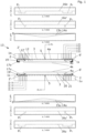
- the Figure 1 shows a bonder 13 according to the invention in a process step according to the invention, from the bonder 13 to the For illustration purposes, only a lower receiving device 1u and an upper receiving device 1o arranged opposite the lower receiving device 1u are shown. The other, usual components of the bonder 13 are not shown.
- a lower plate 17u is fixed on a first plate side 20 by means of ring-shaped first fixing elements 2 of the lower receiving device 1u.
- the fixing elements 2 can in particular be acted upon by fluid technology, preferably with channels that can be acted upon by pressure and pass through the receiving device 1u.
- the lower plate 17u has second fixing elements 2' on a plate side 21 opposite the first plate side 20, which can preferably be controlled directly by the lower receiving device 1u and/or are connected to the first fixing elements 2.
- the upper receiving device 1o also has an upper plate 17o, which can be fixed by means of ring-shaped fixing elements 2 of the upper receiving device 1o.
- the second fixing elements 2' of the plates 17u, 17o are connected to the receiving device 1o, 1u via fixing element connections 6'.
- the fixing element connections 6' are preferably designed as channels, in particular passing through the plates 17u, 17o.
- the fixing element connections 6' of the lower plate 17u are also evacuated, in particular automatically. The same applies to the upper plate 17o and the upper receiving device 1o.
- the plates 17u, 17o are in a curved state because within the ring-shaped fixing elements 2, curvature elements 5 cause a curvature, while the fixing elements 2 fix the plates 17u, 17o.
- a first (upper) substrate 4o is fixed to the upper plate 17o by the fixing elements 2'.
- a second (lower) substrate 4u is fixed to the lower plate 17u by the fixing elements 2'.
- First diagrams in the Figure 1 Above and below the bonder 13 represent an actual curvature 14u, 14o of the substrates 4u, 4o and/or the plates 17u, 17o as well as a desired curvature 15u, 15o of the substrates 4u, 4o and/or the plates 17u, 17o as a function of the x-position.
- second diagrams are shown in Figure 1 which represent a pressure p 1' which drops across the fixing element connections 6' designed as lines and which fixes the substrates 4u, 4o to the plates 17u, 17o.
- the third diagrams show the pressure p 1 which is present at the periphery of the plates 4u, 4o.
- First limiting elements 19' are located on the lower receiving device 1u, which limit a purely translational displacement of the plate 17u according to the invention. It is conceivable, for example, that in one process step all the fixings 2 are switched off and the lower plate 17u floats freely on an air cushion that is generated by a fluid that emerges in particular from the curvature element 5.
- Second limiting elements 19 are located on the upper receiving device 1o and are shaped in such a way that they prevent the plate 17o from falling down, in particular with the substrate 4o fixed thereon.
- an upper receiving device 1o is carried out with the help of a particularly stretchable fixing element connection 6" (in Figure 1 not shown) an independent control of the second fixing element 2 (channel subjected to pressure p 1 ) of the receiving device 1u Fixing elements 2'. This can be subjected to a pressure p 1' via a pressure line.
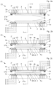
- the Figure 2a shows a bonder 13 according to the invention for contacting and bonding contact surfaces 4k of a first/upper substrate 4o and a second/lower substrate 4u arranged opposite one another.
- the bonder 13 consists of a lower receiving device 1u and an upper receiving device 1o.
- the receiving devices 1u, 1o can be designed in particular to receive a first/upper substrate 4o and/or a first/upper plate 17o and a second/lower substrate 4u and/or a second/lower plate 17u, wherein the lower receiving device 1u can be designed or equipped differently than the upper receiving device 1o.
- the upper receiving device 1o preferably has measurement holes 12 through which, in particular from a rear side of the substrate holder 1o, a measurement of the plate 17o and/or the substrate 4o can take place. If the substrate 4o is measured, in particular the plate 17o also has corresponding measurement holes 12'. Alternatively, sensors can be arranged in the measurement holes 12, 12'. The measurement holes 12, 12' are arranged in particular between the curvature changing means and the fixing means. Alternatively or additionally, the lower substrate holder 1u and/or the lower plate 17u can have corresponding measurement holes 12, 12'. The measurement holes pass through the receiving device 1 and run in particular orthogonal to the receiving surface 1s. Preferably, the surveying holes 12 are arranged at a distance of 180° or 120° from each other on the surface.
- the receiving devices 1u, 1o have a receiving surface 1s with several fixing elements 2 and sensors 3, 3'.
- the fixing elements 2 are evacuated via channels designed as fluid lines and fix the plates 17u, 17o.
- the distance sensors are arranged directly on the curvature changing means 5 and distributed up to the fixing means. They thus extend over a partial area of the receiving surface 1s.
- sensors 3' designed as pressure sensors are arranged, with which the pressures p 1 are measured along the x-position of the sensors 3 between the plates 17u, 17o and the receiving devices 1u, 1o.
- the upper substrate 4o has an actual curvature 14o, which is present in particular due to gravity, while the lower substrate 1u lies flat and therefore has no actual curvature 14u (in reality a vanishingly small one) in the sense of the present invention.
- the gravitationally set actual curvature 14o is negligibly small.
- the Figure 2b shows the bonder 13 during a further process step.
- the two substrates 4u and 4o were brought closer together by a relative movement of the two substrate holders 1u, 1o. Otherwise, the situation has changed compared to the situation according to Figure 2a nothing changed.
- the Figure 2c shows the bonder 13 in a further process step.
- the curvature elements 5 in the case shown a gas outlet opening through which a gas flows at a pressure p2
- the two plates 17u, 17o and thus the substrates 1u, 1o are brought into a desired curvature, wherein preferably a regulation of the pressure by means of the distance sensors.
- the pressures of the fixing elements 2 can also be used for the control/regulation, so that they also take on tasks of the curvature means 5, 5' or curvature changing means 5, 5' and can therefore also be counted among these in the sense of the invention.
- the pressure values can be controlled/regulated in particular continuously and/or steadily, preferably separately in zones.
- the Figure 2d shows the bonder 13 in a further process step.
- the two substrates 4u, 4o approach each other, the two substrates 4u, 4o form a bonding wave that spreads radially outwards, with the curvature of the substrates 4u, 4o changing continuously (curvature changing means).
- the change in curvature of the lower and/or upper plate 17u, 17o or the lower and/or upper substrate 1u, 1o is continuously monitored by means of the distance sensors and, if necessary, corrected by the curvature element 5 and/or the fixing elements 2 so that the desired or set target curvature is achieved (curvature changing means).
- Important parameters are the radii of curvature R1 of the upper plate 17o or the upper substrate 4o and R2 of the lower plate 17u or the lower substrate 4u at the point of the bonding wave.
- the pressures of four inner circumferential rows of fixing elements 2 are reduced to p0 at the upper receiving device 1o and the lower receiving device 1u simultaneously.
- the substrates 1u, 1o or the plates 17u, 17o lose the fixation to the receiving surface 1o, in particular continuously from the inside to the outside, whereby the pressure p2 from the curvature element 5 can spread further.
- run-out errors are minimized.
- "run-out" errors are further minimized because the plate-substrate system has a higher bending resistance and thus the substrate bonds more stably to the opposite substrate.
- the Figure 2e shows the bonder 13 in a further process step.
- the two substrates 1u, 1o have been bonded together in a controlled manner by reducing the pressure of the outermost row of fixing elements 2 of the upper receiving device 1o to p0.
- the upper plate 17o was left on the upper receiving device 1o. It is also conceivable that the upper plate 17o remains on the upper substrate 4o. In this case, no limiting elements 19 should be present.
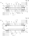
- the Figure 3 shows an improved and more preferred embodiment of the invention of a receiving device 1u and a plate 17u, in which the fixation is transferred from the receiving device 1u to the plate 17u via a fixing element connection 6", designed in particular as a bellows or lip.
- the fixing element device 6" is in particular stretchable without interrupting the fixation of a substrate 4u to the plate 17u.
- the fixing element connection 6" could, for example, be rods which maintain the potential between the receiving device 1u and the plate 17u.
- the fixing element connection 6" is a stretchable bellows, in particular as vacuum-tight as possible. If the fixing element connection 6" is mounted in particular centrally, possible curvature elements 5 are located to the side of the fixing element connection 6".
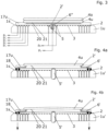
- the Figure 4a shows a recording device 1u', which is constructed similarly to the recording device 1u, in a first process step according to the invention.
- a distinguishing feature is the Receiving device 1u' in particular has sealing rings 18 arranged in a ring shape.
- the plate 17u is mounted on the sealing rings 18.
- a pin is arranged in the center of the receiving device 1u' as the curvature element 5'.
- the pin passes through the receiving device 1u' in the center and is movable relative to it in a z-direction.
- the plate 17u with the substrate 4u is placed on the tip of the already raised curvature element 5'.
- the plate is still lying on undeformed sealing rings 18.
- the plate 17u is essentially not yet curved.
- the Figure 4b shows the receiving device 1u' in a second process step. By switching on the vacuum along a vacuum path (channels, fixing elements 2, fixing element connections 6', 6", fixing elements 2'), the plate 17u is pulled downwards at the edge.
- FIG. 3a, 3b can be considered as a kinematic inversion of the embodiments of the Figures 1-2e
- this embodiment is characterized in that the plate 17u is also pulled downwards at the periphery by the generation of a vacuum, which acts in particular on the periphery, while in previous embodiments it was described how the application of force by the curvature element 5 leads to the plate 17u being deformed in the region of the curvature element 5 by distribution of the fluid flowing in through the curvature element 5.
Landscapes
- Container, Conveyance, Adherence, Positioning, Of Wafer (AREA)
- Combinations Of Printed Boards (AREA)
Claims (16)
- Procédé de collage d'un premier substrat (4o) avec un second substrat (4u) sur des surfaces de contact (4k) des substrats (4o, 4u) tournées l'une vers l'autre, dans lequel le premier substrat (4o) est reçu sur un premier dispositif de réception (1o) et le second substrat (4u) est reçu sur un second dispositif de réception (1u), dans lequel le second dispositif de réception (1u) présente une plaque (17u) et dans lequel la plaque (17u) est disposée entre le second substrat (4u) et une surface du second dispositif de réception (1u),
caractérisé en ce que
le second substrat (4u) est déformé par rapport au second dispositif de réception (1u) avec la plaque (17u) avant et/ou pendant le collage, dans lequel le second substrat (4u) est déformé par une déformation de la plaque (17u), dans lequel la plaque (17u) est fixée par des premiers moyens de fixation (2) disposés sur le pourtour du dispositif de réception (1o, 1u). - Procédé selon la revendication 1, dans lequel une plaque (17o) est disposée entre le premier substrat (4o) et le premier dispositif de réception (1o), dans lequel le premier substrat (4o) est déformé par rapport au premier dispositif de réception (1o) avec la plaque (17o) avant et/ou pendant le collage.
- Procédé selon l'une des revendications précédentes, dans lequel, avant la mise en contact avec les surfaces de contact (4k), la déformation est réglée et/ou conduite en symétrie de miroir et/ou de manière concentrique aux surfaces de contact (4k).
- Procédé selon l'une des revendications précédentes, dans lequel au moins une des déformations, en particulier par alimentation en fluide sous pression, est réglée et/ou conduite au moyen d'au moins un moyen de flexion (5, 5') sollicitant la plaque (17u, 17o).
- Procédé selon l'une des revendications précédentes, dans lequel au moins une des plaques (17u, 17o) est fixée par des premiers moyens de fixation (2) disposés de manière annulaire, principalement en arc de cercle, sur le pourtour des dispositifs de réception (1u, 1o), en particulier exclusivement au niveau du bord de pourtour de la plaque (17o, 17u).
- Procédé selon la revendication 5, dans lequel au moins un des substrats (4u, 4o) est fixé par des seconds moyens de fixation (2') de la plaque (17o, 17u) de préférence similaires, reliés en particulier aux premiers moyens de fixation (2) du dispositif de réception.
- Procédé selon l'une des revendications précédentes, dans lequel la déformation d'au moins un des substrats (4o, 4u) et/ou d'au moins une des plaques (17o, 17u) est détectée par des moyens de détection de flexion, en particulier des capteurs (3), de préférence des capteurs de distance.
- Procédé selon au moins l'une des revendications précédentes, dans lequel un rayon de courbure de la plaque (17u) est réglable.
- Dispositif pour coller un premier substrat (4o) avec un second substrat (4u) sur des surfaces de contact (4k) des substrats (4o, 4u) tournées l'une vers l'autre, comprenant :- un premier dispositif de réception (1o) pour recevoir le premier substrat (4o) et un second dispositif de réception (1u) pour recevoir le second substrat (4u), dans lequel le second dispositif de réception (1u) présente une plaque (17u),- dans lequel la plaque (17u) est disposée entre le second substrat (4u) et le second dispositif de réception (1u),caractérisé en ce que le second substrat (4u) peut être déformé par rapport au second dispositif de réception (1u) avec la plaque (17u) avant et/ou pendant le collage, dans lequeldes moyens de modification de la courbure pour déformer la plaque (17u) avec le second substrat (4u) par rapport au second dispositif de réception (1u) pendant le collage peuvent être commandés,dans lequel le second substrat (4u) peut être déformé par une déformation de la plaque (17u), dans lequel la plaque (17u) est fixée par des premiers moyens de fixation (2) disposés sur le pourtour du dispositif de réception (1o, 1u).
- Dispositif selon la revendication 9, dans lequel une plaque (17o) est disposée entre le premier substrat (4o) et le premier dispositif de réception (1o), dans lequel le premier substrat (4o) est conçu en pouvant être déformé par rapport au premier dispositif de réception (1o) avec la plaque (17o) avant et/ou pendant le collage.
- Dispositif selon la revendication 9 ou 10, dans lequel le premier dispositif de réception (1o) et/ou le second dispositif de réception (1u) présentent des moyens de flexion en particulier mécaniques, et/ou des moyens d'alimentation en fluide sous pression pour régler et/ou commander les déformations.
- Dispositif selon au moins l'une des revendications précédentes, dans lequel le premier dispositif de réception (1o) et/ou le second dispositif de réception (1u) présentent des premiers moyens de fixation (2) disposés de manière annulaire, pour fixer la plaque (17o, 17u).
- Dispositif selon au moins l'une des revendications précédentes, dans lequel au moins une des plaques, présente des seconds moyens de fixation (2') de préférence similaires, reliés en particulier aux premiers moyens de fixation (2) du dispositif de réception (1o, 1u) pour fixer les substrats (4u, 4o).
- Dispositif selon au moins l'une des revendications précédentes, dans lequel au moins une des plaques (17o, 17u) présente un module d'élasticité entre 0,01 GPa et 1100 GPa, de préférence entre 0,1 GPa et 800 GPa, plus encore de préférence entre 1 GPa et 600 GPa, de manière la plus préférée entre 10 GPa et 500 GPa, de manière préférée entre toutes entre 100 GPa et 450 GPa.
- Dispositif selon au moins l'une des revendications précédentes, dans lequel les déformations peuvent être détectées par des moyens de mesure de flexion, en particulier des capteurs, de préférence des capteurs de distance.
- Dispositif selon au moins l'une des revendications précédentes, dans lequel un rayon de courbure de la plaque (17u) est réglable.
Priority Applications (2)
| Application Number | Priority Date | Filing Date | Title |
|---|---|---|---|
| EP24204876.7A EP4465340A3 (fr) | 2017-09-21 | 2017-09-21 | Dispositif et procédé de liaison de substrats |
| EP19215305.4A EP3640975B1 (fr) | 2017-09-21 | 2017-09-21 | Dispositif et procédé de liaison de substrats |
Applications Claiming Priority (3)
| Application Number | Priority Date | Filing Date | Title |
|---|---|---|---|
| PCT/EP2017/073930 WO2019057286A1 (fr) | 2017-09-21 | 2017-09-21 | Dispositif et procédé de bonding de substrats |
| EP19215305.4A EP3640975B1 (fr) | 2017-09-21 | 2017-09-21 | Dispositif et procédé de liaison de substrats |
| EP17783732.5A EP3501037B1 (fr) | 2017-09-21 | 2017-09-21 | Appareil et méthode pour liaison de substrats |
Related Parent Applications (2)
| Application Number | Title | Priority Date | Filing Date |
|---|---|---|---|
| EP17783732.5A Division EP3501037B1 (fr) | 2017-09-21 | 2017-09-21 | Appareil et méthode pour liaison de substrats |
| EP17783732.5A Division-Into EP3501037B1 (fr) | 2017-09-21 | 2017-09-21 | Appareil et méthode pour liaison de substrats |
Related Child Applications (2)
| Application Number | Title | Priority Date | Filing Date |
|---|---|---|---|
| EP24204876.7A Division EP4465340A3 (fr) | 2017-09-21 | 2017-09-21 | Dispositif et procédé de liaison de substrats |
| EP24204876.7A Division-Into EP4465340A3 (fr) | 2017-09-21 | 2017-09-21 | Dispositif et procédé de liaison de substrats |
Publications (2)
| Publication Number | Publication Date |
|---|---|
| EP3640975A1 EP3640975A1 (fr) | 2020-04-22 |
| EP3640975B1 true EP3640975B1 (fr) | 2024-11-20 |
Family
ID=60083251
Family Applications (3)
| Application Number | Title | Priority Date | Filing Date |
|---|---|---|---|
| EP19215305.4A Active EP3640975B1 (fr) | 2017-09-21 | 2017-09-21 | Dispositif et procédé de liaison de substrats |
| EP24204876.7A Pending EP4465340A3 (fr) | 2017-09-21 | 2017-09-21 | Dispositif et procédé de liaison de substrats |
| EP17783732.5A Active EP3501037B1 (fr) | 2017-09-21 | 2017-09-21 | Appareil et méthode pour liaison de substrats |
Family Applications After (2)
| Application Number | Title | Priority Date | Filing Date |
|---|---|---|---|
| EP24204876.7A Pending EP4465340A3 (fr) | 2017-09-21 | 2017-09-21 | Dispositif et procédé de liaison de substrats |
| EP17783732.5A Active EP3501037B1 (fr) | 2017-09-21 | 2017-09-21 | Appareil et méthode pour liaison de substrats |
Country Status (8)
| Country | Link |
|---|---|
| US (3) | US11315901B2 (fr) |
| EP (3) | EP3640975B1 (fr) |
| JP (4) | JP7123123B2 (fr) |
| KR (7) | KR102183296B1 (fr) |
| CN (7) | CN118099000A (fr) |
| SG (1) | SG11201909992QA (fr) |
| TW (8) | TWI797024B (fr) |
| WO (1) | WO2019057286A1 (fr) |
Families Citing this family (26)
| Publication number | Priority date | Publication date | Assignee | Title |
|---|---|---|---|---|
| US11355666B2 (en) | 2019-05-07 | 2022-06-07 | Facebook Technologies, Llc | Bonding methods for light emitting diodes |
| KR102760924B1 (ko) * | 2019-05-20 | 2025-02-03 | 삼성전자주식회사 | 기판 본딩 장치 및 이를 이용한 반도체 소자 제조 방법 |
| SG11201911798UA (en) | 2019-08-23 | 2021-04-29 | Ev Group E Thallner Gmbh | Method and device for the alignment of substrates |
| KR102734318B1 (ko) * | 2019-11-08 | 2024-11-25 | 에베 그룹 에. 탈너 게엠베하 | 기판 결합 장치 및 방법 |
| US12482678B2 (en) | 2019-12-02 | 2025-11-25 | Ev Group E. Thallner Gmbh | Apparatus with deformable heater and method for heating a substrate thereof |
| JP7507860B2 (ja) | 2019-12-10 | 2024-06-28 | エーファウ・グループ・エー・タルナー・ゲーエムベーハー | 複数の基板の位置合わせをする方法および装置 |
| JP7368263B2 (ja) * | 2020-02-14 | 2023-10-24 | 株式会社Screenホールディングス | 基板処理装置および基板処理方法 |
| KR20230029607A (ko) | 2020-06-29 | 2023-03-03 | 에베 그룹 에. 탈너 게엠베하 | 기판 홀더 및 기판 고정 및 접합 방법 |
| KR102775379B1 (ko) * | 2020-06-29 | 2025-02-28 | 에베 그룹 에. 탈너 게엠베하 | 기판 접합 방법 및 장치 |
| US11587795B2 (en) * | 2020-09-28 | 2023-02-21 | Canon Kabushiki Kaisha | Planarization apparatus including superstrate chuck with bendable periphery |
| EP4232854A1 (fr) * | 2020-10-23 | 2023-08-30 | Corning Incorporated | Dispositif et procédé de fabrication d'un dispositif, tel qu'une lentille liquide, avec des liaisons configurées pour se rompre à la même pression de rupture |
| JP7678099B2 (ja) | 2021-02-01 | 2025-05-15 | エーファウ・グループ・エー・タルナー・ゲーエムベーハー | 基板ホルダおよび接合のための基板ホルダを製造する方法 |
| KR102883385B1 (ko) * | 2021-02-10 | 2025-11-07 | 주식회사 제우스 | 기판 본딩 장치와 방법 |
| TWI802956B (zh) * | 2021-08-11 | 2023-05-21 | 日商雅馬哈智能機器控股股份有限公司 | 部材間接合裝置以及接合部材製造方法 |
| JP7712832B2 (ja) | 2021-09-21 | 2025-07-24 | キヤノン株式会社 | インプリント装置、インプリント方法、および物品の製造方法 |
| JP7710350B2 (ja) * | 2021-09-28 | 2025-07-18 | キヤノン株式会社 | インプリント方法、インプリント装置、および物品の製造方法 |
| CN117941048A (zh) * | 2021-11-08 | 2024-04-26 | Ev 集团 E·索尔纳有限责任公司 | 用于接合基板的设备和方法 |
| CN116403929A (zh) * | 2021-12-28 | 2023-07-07 | 拓荆键科(海宁)半导体设备有限公司 | 调整卡盘形变的系统及装置 |
| JP2024020064A (ja) * | 2022-08-01 | 2024-02-14 | 株式会社ディスコ | リフトオフ方法 |
| WO2024046577A1 (fr) | 2022-09-02 | 2024-03-07 | Ev Group E. Thallner Gmbh | Procédé et dispositif pour influencer une onde de liaison lors d'une liaison |
| KR20240147798A (ko) | 2023-03-30 | 2024-10-10 | 세메스 주식회사 | 웨이퍼 변형 기구, 웨이퍼 본딩 장치, 및 웨이퍼 본딩 방법 |
| JP2024165113A (ja) * | 2023-05-16 | 2024-11-28 | 株式会社Screenホールディングス | 基板接合装置 |
| JP7695433B1 (ja) | 2024-03-08 | 2025-06-18 | タツモ株式会社 | 貼合装置 |
| WO2025214610A1 (fr) | 2024-04-12 | 2025-10-16 | Ev Group E. Thallner Gmbh | Support de substrat, procédé de fabrication d'un support de substrat de ce type, et procédé de maintien d'un substrat |
| WO2025228529A1 (fr) | 2024-05-02 | 2025-11-06 | Ev Group E. Thallner Gmbh | Support de substrat et procédé de fabrication d'un support de substrat |
| WO2026046508A1 (fr) | 2024-08-28 | 2026-03-05 | Ev Group E. Thallner Gmbh | Procédé de liaison d'un premier substrat sur un second substrat, support de substrat pour un tel procédé, et dispositif comprenant un tel support de substrat |
Family Cites Families (40)
| Publication number | Priority date | Publication date | Assignee | Title |
|---|---|---|---|---|
| JPS61145839A (ja) * | 1984-12-20 | 1986-07-03 | Toshiba Corp | 半導体ウエ−ハの接着方法および接着治具 |
| US5273553A (en) * | 1989-08-28 | 1993-12-28 | Kabushiki Kaisha Toshiba | Apparatus for bonding semiconductor substrates |
| JPH0766093A (ja) * | 1993-08-23 | 1995-03-10 | Sumitomo Sitix Corp | 半導体ウエーハの貼り合わせ方法およびその装置 |
| JPH1174164A (ja) * | 1997-08-27 | 1999-03-16 | Canon Inc | 基板処理装置、基板支持装置及び基板処理方法並びに基板の製造方法 |
| SG71182A1 (en) * | 1997-12-26 | 2000-03-21 | Canon Kk | Substrate processing apparatus substrate support apparatus substrate processing method and substrate manufacturing method |
| AT405775B (de) | 1998-01-13 | 1999-11-25 | Thallner Erich | Verfahren und vorrichtung zum ausgerichteten zusammenführen von scheibenförmigen halbleitersubstraten |
| JP3947989B2 (ja) | 1998-10-21 | 2007-07-25 | 株式会社エンヤシステム | マウント板へのウエ−ハ接着方法及び装置 |
| US20020110328A1 (en) * | 2001-02-14 | 2002-08-15 | Bischel William K. | Multi-channel laser pump source for optical amplifiers |
| FR2848337B1 (fr) * | 2002-12-09 | 2005-09-09 | Commissariat Energie Atomique | Procede de realisation d'une structure complexe par assemblage de structures contraintes |
| JP5281739B2 (ja) | 2006-07-18 | 2013-09-04 | 新光電気工業株式会社 | 陽極接合装置 |
| JP2009010072A (ja) | 2007-06-27 | 2009-01-15 | Shinko Electric Ind Co Ltd | 基板貼付装置 |
| KR20100108418A (ko) | 2008-11-14 | 2010-10-06 | 도쿄엘렉트론가부시키가이샤 | 접합 장치 및 접합 방법 |
| EP2351076B1 (fr) * | 2008-11-16 | 2016-09-28 | Suss MicroTec Lithography GmbH | Procédé et appareil de liaison de plaquette à connexion de plaquette améliorée |
| US8366873B2 (en) * | 2010-04-15 | 2013-02-05 | Suss Microtec Lithography, Gmbh | Debonding equipment and methods for debonding temporary bonded wafers |
| KR20120027237A (ko) * | 2009-04-16 | 2012-03-21 | 수스 마이크로텍 리소그라피 게엠바하 | 웨이퍼 가접합 및 분리를 위한 개선된 장치 |
| FR2962594B1 (fr) | 2010-07-07 | 2012-08-31 | Soitec Silicon On Insulator | Procede de collage par adhesion moleculaire avec compensation de desalignement radial |
| FR2965398B1 (fr) | 2010-09-23 | 2012-10-12 | Soitec Silicon On Insulator | Procédé de collage par adhésion moléculaire avec réduction de desalignement de type overlay |
| JP6279324B2 (ja) * | 2010-12-20 | 2018-02-14 | エーファウ・グループ・エー・タルナー・ゲーエムベーハー | ウェハの装着用受け取り手段 |
| JP5558452B2 (ja) | 2011-10-21 | 2014-07-23 | 東京エレクトロン株式会社 | 貼り合わせ装置 |
| JP5606429B2 (ja) * | 2011-12-08 | 2014-10-15 | 東京エレクトロン株式会社 | 接合方法、プログラム、コンピュータ記憶媒体、接合装置及び接合システム |
| JP2013187393A (ja) | 2012-03-08 | 2013-09-19 | Tokyo Electron Ltd | 貼り合わせ装置及び貼り合わせ方法 |
| JP2013258377A (ja) * | 2012-06-14 | 2013-12-26 | Sony Corp | 半導体装置の製造装置および半導体装置の製造方法 |
| US9538582B2 (en) | 2012-07-26 | 2017-01-03 | Taiwan Semiconductor Manufacturing Company, Ltd. | Warpage control in the packaging of integrated circuits |
| JP6501447B2 (ja) * | 2013-03-26 | 2019-04-17 | 芝浦メカトロニクス株式会社 | 貼合装置および貼合基板の製造方法 |
| CN109616408B (zh) | 2013-05-29 | 2023-07-25 | Ev 集团 E·索尔纳有限责任公司 | 用以接合衬底的装置及方法 |
| SG2014014054A (en) | 2013-06-17 | 2014-10-30 | Ev Group E Thallner Gmbh | Device and Method for Alignment of substrates |
| CN105247670B (zh) | 2013-12-06 | 2018-06-12 | Ev 集团 E·索尔纳有限责任公司 | 用于对齐衬底的装置和方法 |
| US9837291B2 (en) | 2014-01-24 | 2017-12-05 | Taiwan Semiconductor Manufacturing Company, Ltd. | Wafer processing method and apparatus |
| KR102009551B1 (ko) | 2014-02-03 | 2019-08-09 | 에베 그룹 에. 탈너 게엠베하 | 기질을 결합하기 위한 방법 및 장치 |
| US9576827B2 (en) * | 2014-06-06 | 2017-02-21 | Taiwan Semiconductor Manufacturing Company, Ltd. | Apparatus and method for wafer level bonding |
| JP6177739B2 (ja) | 2014-08-07 | 2017-08-09 | 東京エレクトロン株式会社 | 接合装置、接合システム、接合方法、プログラム及びコンピュータ記憶媒体 |
| WO2016093284A1 (fr) | 2014-12-10 | 2016-06-16 | 株式会社ニコン | Dispositif et procédé d'empilement de substrats |
| US9490158B2 (en) * | 2015-01-08 | 2016-11-08 | Taiwan Semiconductor Manufacturing Company, Ltd. | Bond chuck, methods of bonding, and tool including bond chuck |
| KR20170137050A (ko) | 2015-04-10 | 2017-12-12 | 에베 그룹 에. 탈너 게엠베하 | 2개의 기판을 결합하기 위한 기판 홀더 및 방법. |
| JP6407803B2 (ja) | 2015-06-16 | 2018-10-17 | 東京エレクトロン株式会社 | 接合装置、接合システム、接合方法、プログラム及びコンピュータ記憶媒体 |
| JP6616181B2 (ja) * | 2015-12-25 | 2019-12-04 | 東京エレクトロン株式会社 | 接合装置 |
| SG11201702778YA (en) | 2016-02-16 | 2017-09-28 | Ev Group E Thallner Gmbh | Method for bonding substrates |
| JP6448848B2 (ja) | 2016-03-11 | 2019-01-09 | ボンドテック株式会社 | 基板接合方法 |
| KR102749376B1 (ko) * | 2016-11-02 | 2025-01-06 | 삼성전자주식회사 | 기판 본딩 장치 및 그를 이용한 반도체 소자의 제조 방법 |
| JP6671518B2 (ja) * | 2017-02-02 | 2020-03-25 | 三菱電機株式会社 | 半導体製造方法および半導体製造装置 |
-
2017
- 2017-09-21 CN CN202410064010.5A patent/CN118099000A/zh active Pending
- 2017-09-21 CN CN202410063997.9A patent/CN118098996A/zh active Pending
- 2017-09-21 KR KR1020187026946A patent/KR102183296B1/ko active Active
- 2017-09-21 JP JP2020505485A patent/JP7123123B2/ja active Active
- 2017-09-21 CN CN202410064002.0A patent/CN118098998A/zh active Pending
- 2017-09-21 KR KR1020237004974A patent/KR102656787B1/ko active Active
- 2017-09-21 CN CN202410064013.9A patent/CN118099001A/zh active Pending
- 2017-09-21 SG SG11201909992Q patent/SG11201909992QA/en unknown
- 2017-09-21 WO PCT/EP2017/073930 patent/WO2019057286A1/fr not_active Ceased
- 2017-09-21 US US16/632,643 patent/US11315901B2/en active Active
- 2017-09-21 KR KR1020217020666A patent/KR102385071B1/ko active Active
- 2017-09-21 CN CN202410064007.3A patent/CN118098999A/zh active Pending
- 2017-09-21 EP EP19215305.4A patent/EP3640975B1/fr active Active
- 2017-09-21 CN CN201780025114.3A patent/CN110168711B/zh active Active
- 2017-09-21 EP EP24204876.7A patent/EP4465340A3/fr active Pending
- 2017-09-21 KR KR1020217010482A patent/KR102274677B1/ko active Active
- 2017-09-21 CN CN202410063999.8A patent/CN118098997A/zh active Pending
- 2017-09-21 EP EP17783732.5A patent/EP3501037B1/fr active Active
- 2017-09-21 KR KR1020207033389A patent/KR102240536B1/ko active Active
- 2017-09-21 KR KR1020247011567A patent/KR102923694B1/ko active Active
- 2017-09-21 KR KR1020227011210A patent/KR102500460B1/ko active Active
-
2018
- 2018-08-15 TW TW111122282A patent/TWI797024B/zh active
- 2018-08-15 TW TW112104993A patent/TWI810135B/zh active
- 2018-08-15 TW TW110111309A patent/TWI774292B/zh active
- 2018-08-15 TW TW113116777A patent/TWI896118B/zh active
- 2018-08-15 TW TW107128408A patent/TWI673816B/zh active
- 2018-08-15 TW TW114128441A patent/TW202546934A/zh unknown
- 2018-08-15 TW TW112123342A patent/TW202345241A/zh unknown
- 2018-08-15 TW TW108130088A patent/TWI773917B/zh active
-
2022
- 2022-02-15 US US17/671,732 patent/US12412865B2/en active Active
- 2022-08-09 JP JP2022126879A patent/JP7459184B2/ja active Active
-
2024
- 2024-03-19 JP JP2024044179A patent/JP7845616B2/ja active Active
-
2025
- 2025-08-14 US US19/299,651 patent/US20250372571A1/en active Pending
- 2025-11-10 JP JP2025189351A patent/JP2026027413A/ja active Pending
Also Published As
Similar Documents
| Publication | Publication Date | Title |
|---|---|---|
| EP3501037B1 (fr) | Appareil et méthode pour liaison de substrats | |
| EP3433875B1 (fr) | Procédé de liaison de substrats | |
| EP3404698B1 (fr) | Procédé de liaison des substrats | |
| EP3497712B1 (fr) | Procédé et porte-échantillon pour lier des substrats de façon commandée | |
| EP2422364B1 (fr) | Dispositif d'orientation et de préfixation d'une tranche | |
| EP3140856B1 (fr) | Procédé et dispositif de liaison permanente | |
| WO2024046578A1 (fr) | Support de substrat sous vide à joint à vide optimisé | |
| DE102008052100B4 (de) | Flexibel verformbares Halteelement für Substrate | |
| WO2026046508A1 (fr) | Procédé de liaison d'un premier substrat sur un second substrat, support de substrat pour un tel procédé, et dispositif comprenant un tel support de substrat | |
| EP4487371A1 (fr) | Dispositif et procédé de fixation d'un substrat | |
| WO2025228529A1 (fr) | Support de substrat et procédé de fabrication d'un support de substrat | |
| EP4548384A1 (fr) | Procédé de liaison d'un premier substrat à un second substrat, dispositif de liaison et d'assemblage d'un premier et d'un second substrat | |
| DE102015100608A1 (de) | Verfahren und Vorrichtung zur Bearbeitung eines Substrats |
Legal Events
| Date | Code | Title | Description |
|---|---|---|---|
| PUAI | Public reference made under article 153(3) epc to a published international application that has entered the european phase |
Free format text: ORIGINAL CODE: 0009012 |
|
| STAA | Information on the status of an ep patent application or granted ep patent |
Free format text: STATUS: THE APPLICATION HAS BEEN PUBLISHED |
|
| AC | Divisional application: reference to earlier application |
Ref document number: 3501037 Country of ref document: EP Kind code of ref document: P |
|
| AK | Designated contracting states |
Kind code of ref document: A1 Designated state(s): AL AT BE BG CH CY CZ DE DK EE ES FI FR GB GR HR HU IE IS IT LI LT LU LV MC MK MT NL NO PL PT RO RS SE SI SK SM TR |
|
| STAA | Information on the status of an ep patent application or granted ep patent |
Free format text: STATUS: REQUEST FOR EXAMINATION WAS MADE |
|
| 17P | Request for examination filed |
Effective date: 20200909 |
|
| RBV | Designated contracting states (corrected) |
Designated state(s): AL AT BE BG CH CY CZ DE DK EE ES FI FR GB GR HR HU IE IS IT LI LT LU LV MC MK MT NL NO PL PT RO RS SE SI SK SM TR |
|
| STAA | Information on the status of an ep patent application or granted ep patent |
Free format text: STATUS: EXAMINATION IS IN PROGRESS |
|
| 17Q | First examination report despatched |
Effective date: 20211021 |
|
| GRAP | Despatch of communication of intention to grant a patent |
Free format text: ORIGINAL CODE: EPIDOSNIGR1 |
|
| STAA | Information on the status of an ep patent application or granted ep patent |
Free format text: STATUS: GRANT OF PATENT IS INTENDED |
|
| RIC1 | Information provided on ipc code assigned before grant |
Ipc: H01L 21/762 20060101ALN20240527BHEP Ipc: H01L 23/00 20060101ALN20240527BHEP Ipc: H01L 21/687 20060101ALN20240527BHEP Ipc: H01L 21/20 20060101ALI20240527BHEP Ipc: H01L 21/18 20060101ALI20240527BHEP Ipc: H01L 21/683 20060101ALI20240527BHEP Ipc: H01L 21/67 20060101AFI20240527BHEP |
|
| INTG | Intention to grant announced |
Effective date: 20240612 |
|
| RIN1 | Information on inventor provided before grant (corrected) |
Inventor name: PLACH, THOMAS Inventor name: SUESS, JUERGEN MARKUS Inventor name: WAGENLEITNER, THOMAS Inventor name: ZINNER, DOMINIK |
|
| GRAS | Grant fee paid |
Free format text: ORIGINAL CODE: EPIDOSNIGR3 |
|
| GRAA | (expected) grant |
Free format text: ORIGINAL CODE: 0009210 |
|
| STAA | Information on the status of an ep patent application or granted ep patent |
Free format text: STATUS: THE PATENT HAS BEEN GRANTED |
|
| AC | Divisional application: reference to earlier application |
Ref document number: 3501037 Country of ref document: EP Kind code of ref document: P |
|
| AK | Designated contracting states |
Kind code of ref document: B1 Designated state(s): AL AT BE BG CH CY CZ DE DK EE ES FI FR GB GR HR HU IE IS IT LI LT LU LV MC MK MT NL NO PL PT RO RS SE SI SK SM TR |
|
| REG | Reference to a national code |
Ref country code: GB Ref legal event code: FG4D Free format text: NOT ENGLISH |
|
| REG | Reference to a national code |
Ref country code: CH Ref legal event code: EP |
|
| REG | Reference to a national code |
Ref country code: DE Ref legal event code: R096 Ref document number: 502017016574 Country of ref document: DE |
|
| REG | Reference to a national code |
Ref country code: IE Ref legal event code: FG4D Free format text: LANGUAGE OF EP DOCUMENT: GERMAN |
|
| REG | Reference to a national code |
Ref country code: NL Ref legal event code: FP |
|
| REG | Reference to a national code |
Ref country code: LT Ref legal event code: MG9D |
|
| PG25 | Lapsed in a contracting state [announced via postgrant information from national office to epo] |
Ref country code: PT Free format text: LAPSE BECAUSE OF FAILURE TO SUBMIT A TRANSLATION OF THE DESCRIPTION OR TO PAY THE FEE WITHIN THE PRESCRIBED TIME-LIMIT Effective date: 20250320 Ref country code: HR Free format text: LAPSE BECAUSE OF FAILURE TO SUBMIT A TRANSLATION OF THE DESCRIPTION OR TO PAY THE FEE WITHIN THE PRESCRIBED TIME-LIMIT Effective date: 20241120 Ref country code: IS Free format text: LAPSE BECAUSE OF FAILURE TO SUBMIT A TRANSLATION OF THE DESCRIPTION OR TO PAY THE FEE WITHIN THE PRESCRIBED TIME-LIMIT Effective date: 20250320 |
|
| PG25 | Lapsed in a contracting state [announced via postgrant information from national office to epo] |
Ref country code: FI Free format text: LAPSE BECAUSE OF FAILURE TO SUBMIT A TRANSLATION OF THE DESCRIPTION OR TO PAY THE FEE WITHIN THE PRESCRIBED TIME-LIMIT Effective date: 20241120 |
|
| PG25 | Lapsed in a contracting state [announced via postgrant information from national office to epo] |
Ref country code: BG Free format text: LAPSE BECAUSE OF FAILURE TO SUBMIT A TRANSLATION OF THE DESCRIPTION OR TO PAY THE FEE WITHIN THE PRESCRIBED TIME-LIMIT Effective date: 20241120 |
|
| PG25 | Lapsed in a contracting state [announced via postgrant information from national office to epo] |
Ref country code: ES Free format text: LAPSE BECAUSE OF FAILURE TO SUBMIT A TRANSLATION OF THE DESCRIPTION OR TO PAY THE FEE WITHIN THE PRESCRIBED TIME-LIMIT Effective date: 20241120 |
|
| PG25 | Lapsed in a contracting state [announced via postgrant information from national office to epo] |
Ref country code: NO Free format text: LAPSE BECAUSE OF FAILURE TO SUBMIT A TRANSLATION OF THE DESCRIPTION OR TO PAY THE FEE WITHIN THE PRESCRIBED TIME-LIMIT Effective date: 20250220 |
|
| PG25 | Lapsed in a contracting state [announced via postgrant information from national office to epo] |
Ref country code: LV Free format text: LAPSE BECAUSE OF FAILURE TO SUBMIT A TRANSLATION OF THE DESCRIPTION OR TO PAY THE FEE WITHIN THE PRESCRIBED TIME-LIMIT Effective date: 20241120 Ref country code: GR Free format text: LAPSE BECAUSE OF FAILURE TO SUBMIT A TRANSLATION OF THE DESCRIPTION OR TO PAY THE FEE WITHIN THE PRESCRIBED TIME-LIMIT Effective date: 20250221 |
|
| PG25 | Lapsed in a contracting state [announced via postgrant information from national office to epo] |
Ref country code: PL Free format text: LAPSE BECAUSE OF FAILURE TO SUBMIT A TRANSLATION OF THE DESCRIPTION OR TO PAY THE FEE WITHIN THE PRESCRIBED TIME-LIMIT Effective date: 20241120 |
|
| PG25 | Lapsed in a contracting state [announced via postgrant information from national office to epo] |
Ref country code: RS Free format text: LAPSE BECAUSE OF FAILURE TO SUBMIT A TRANSLATION OF THE DESCRIPTION OR TO PAY THE FEE WITHIN THE PRESCRIBED TIME-LIMIT Effective date: 20250220 |
|
| PG25 | Lapsed in a contracting state [announced via postgrant information from national office to epo] |
Ref country code: SM Free format text: LAPSE BECAUSE OF FAILURE TO SUBMIT A TRANSLATION OF THE DESCRIPTION OR TO PAY THE FEE WITHIN THE PRESCRIBED TIME-LIMIT Effective date: 20241120 |
|
| PG25 | Lapsed in a contracting state [announced via postgrant information from national office to epo] |
Ref country code: DK Free format text: LAPSE BECAUSE OF FAILURE TO SUBMIT A TRANSLATION OF THE DESCRIPTION OR TO PAY THE FEE WITHIN THE PRESCRIBED TIME-LIMIT Effective date: 20241120 |
|
| PG25 | Lapsed in a contracting state [announced via postgrant information from national office to epo] |
Ref country code: EE Free format text: LAPSE BECAUSE OF FAILURE TO SUBMIT A TRANSLATION OF THE DESCRIPTION OR TO PAY THE FEE WITHIN THE PRESCRIBED TIME-LIMIT Effective date: 20241120 |
|
| PG25 | Lapsed in a contracting state [announced via postgrant information from national office to epo] |
Ref country code: RO Free format text: LAPSE BECAUSE OF FAILURE TO SUBMIT A TRANSLATION OF THE DESCRIPTION OR TO PAY THE FEE WITHIN THE PRESCRIBED TIME-LIMIT Effective date: 20241120 |
|
| PG25 | Lapsed in a contracting state [announced via postgrant information from national office to epo] |
Ref country code: SK Free format text: LAPSE BECAUSE OF FAILURE TO SUBMIT A TRANSLATION OF THE DESCRIPTION OR TO PAY THE FEE WITHIN THE PRESCRIBED TIME-LIMIT Effective date: 20241120 |
|
| PG25 | Lapsed in a contracting state [announced via postgrant information from national office to epo] |
Ref country code: CZ Free format text: LAPSE BECAUSE OF FAILURE TO SUBMIT A TRANSLATION OF THE DESCRIPTION OR TO PAY THE FEE WITHIN THE PRESCRIBED TIME-LIMIT Effective date: 20241120 |
|
| PG25 | Lapsed in a contracting state [announced via postgrant information from national office to epo] |
Ref country code: IT Free format text: LAPSE BECAUSE OF FAILURE TO SUBMIT A TRANSLATION OF THE DESCRIPTION OR TO PAY THE FEE WITHIN THE PRESCRIBED TIME-LIMIT Effective date: 20241120 |
|
| REG | Reference to a national code |
Ref country code: DE Ref legal event code: R097 Ref document number: 502017016574 Country of ref document: DE |
|
| PG25 | Lapsed in a contracting state [announced via postgrant information from national office to epo] |
Ref country code: SE Free format text: LAPSE BECAUSE OF FAILURE TO SUBMIT A TRANSLATION OF THE DESCRIPTION OR TO PAY THE FEE WITHIN THE PRESCRIBED TIME-LIMIT Effective date: 20241120 |
|
| PLBE | No opposition filed within time limit |
Free format text: ORIGINAL CODE: 0009261 |
|
| STAA | Information on the status of an ep patent application or granted ep patent |
Free format text: STATUS: NO OPPOSITION FILED WITHIN TIME LIMIT |
|
| PGFP | Annual fee paid to national office [announced via postgrant information from national office to epo] |
Ref country code: DE Payment date: 20250919 Year of fee payment: 9 |
|
| PGFP | Annual fee paid to national office [announced via postgrant information from national office to epo] |
Ref country code: NL Payment date: 20250922 Year of fee payment: 9 |
|
| PGFP | Annual fee paid to national office [announced via postgrant information from national office to epo] |
Ref country code: FR Payment date: 20250926 Year of fee payment: 9 Ref country code: AT Payment date: 20250918 Year of fee payment: 9 |
|
| 26N | No opposition filed |
Effective date: 20250821 |
|
| REG | Reference to a national code |
Ref country code: DE Ref legal event code: R079 Ref document number: 502017016574 Country of ref document: DE Free format text: PREVIOUS MAIN CLASS: H01L0021670000 Ipc: H10P0072000000 |
|
| REG | Reference to a national code |
Ref country code: CH Ref legal event code: H13 Free format text: ST27 STATUS EVENT CODE: U-0-0-H10-H13 (AS PROVIDED BY THE NATIONAL OFFICE) Effective date: 20260504 |