EP3663084A1 - Verbundstoff aus metall und harz - Google Patents
Verbundstoff aus metall und harz Download PDFInfo
- Publication number
- EP3663084A1 EP3663084A1 EP18842083.0A EP18842083A EP3663084A1 EP 3663084 A1 EP3663084 A1 EP 3663084A1 EP 18842083 A EP18842083 A EP 18842083A EP 3663084 A1 EP3663084 A1 EP 3663084A1
- Authority
- EP
- European Patent Office
- Prior art keywords
- compound
- group
- resin
- metal
- substrate
- Prior art date
- Legal status (The legal status is an assumption and is not a legal conclusion. Google has not performed a legal analysis and makes no representation as to the accuracy of the status listed.)
- Withdrawn
Links
- 0 CC(N(**)C(N(*[S+]*)C(N*[S+]*)=O)=O)=O Chemical compound CC(N(**)C(N(*[S+]*)C(N*[S+]*)=O)=O)=O 0.000 description 1
Images








Classifications
-
- B—PERFORMING OPERATIONS; TRANSPORTING
- B32—LAYERED PRODUCTS
- B32B—LAYERED PRODUCTS, i.e. PRODUCTS BUILT-UP OF STRATA OF FLAT OR NON-FLAT, e.g. CELLULAR OR HONEYCOMB, FORM
- B32B15/00—Layered products comprising a layer of metal
- B32B15/04—Layered products comprising a layer of metal comprising metal as the main or only constituent of a layer, which is next to another layer of the same or of a different material
- B32B15/08—Layered products comprising a layer of metal comprising metal as the main or only constituent of a layer, which is next to another layer of the same or of a different material of synthetic resin
-
- C—CHEMISTRY; METALLURGY
- C09—DYES; PAINTS; POLISHES; NATURAL RESINS; ADHESIVES; COMPOSITIONS NOT OTHERWISE PROVIDED FOR; APPLICATIONS OF MATERIALS NOT OTHERWISE PROVIDED FOR
- C09J—ADHESIVES; NON-MECHANICAL ASPECTS OF ADHESIVE PROCESSES IN GENERAL; ADHESIVE PROCESSES NOT PROVIDED FOR ELSEWHERE; USE OF MATERIALS AS ADHESIVES
- C09J11/00—Features of adhesives not provided for in group C09J9/00, e.g. additives
- C09J11/02—Non-macromolecular additives
- C09J11/06—Non-macromolecular additives organic
-
- B—PERFORMING OPERATIONS; TRANSPORTING
- B05—SPRAYING OR ATOMISING IN GENERAL; APPLYING FLUENT MATERIALS TO SURFACES, IN GENERAL
- B05D—PROCESSES FOR APPLYING FLUENT MATERIALS TO SURFACES, IN GENERAL
- B05D3/00—Pretreatment of surfaces to which liquids or other fluent materials are to be applied; After-treatment of applied coatings, e.g. intermediate treating of an applied coating preparatory to subsequent applications of liquids or other fluent materials
- B05D3/02—Pretreatment of surfaces to which liquids or other fluent materials are to be applied; After-treatment of applied coatings, e.g. intermediate treating of an applied coating preparatory to subsequent applications of liquids or other fluent materials by baking
-
- B—PERFORMING OPERATIONS; TRANSPORTING
- B05—SPRAYING OR ATOMISING IN GENERAL; APPLYING FLUENT MATERIALS TO SURFACES, IN GENERAL
- B05D—PROCESSES FOR APPLYING FLUENT MATERIALS TO SURFACES, IN GENERAL
- B05D3/00—Pretreatment of surfaces to which liquids or other fluent materials are to be applied; After-treatment of applied coatings, e.g. intermediate treating of an applied coating preparatory to subsequent applications of liquids or other fluent materials
- B05D3/10—Pretreatment of surfaces to which liquids or other fluent materials are to be applied; After-treatment of applied coatings, e.g. intermediate treating of an applied coating preparatory to subsequent applications of liquids or other fluent materials by other chemical means
-
- B—PERFORMING OPERATIONS; TRANSPORTING
- B05—SPRAYING OR ATOMISING IN GENERAL; APPLYING FLUENT MATERIALS TO SURFACES, IN GENERAL
- B05D—PROCESSES FOR APPLYING FLUENT MATERIALS TO SURFACES, IN GENERAL
- B05D7/00—Processes, other than flocking, specially adapted for applying liquids or other fluent materials to particular surfaces or for applying particular liquids or other fluent materials
- B05D7/24—Processes, other than flocking, specially adapted for applying liquids or other fluent materials to particular surfaces or for applying particular liquids or other fluent materials for applying particular liquids or other fluent materials
-
- B—PERFORMING OPERATIONS; TRANSPORTING
- B32—LAYERED PRODUCTS
- B32B—LAYERED PRODUCTS, i.e. PRODUCTS BUILT-UP OF STRATA OF FLAT OR NON-FLAT, e.g. CELLULAR OR HONEYCOMB, FORM
- B32B15/00—Layered products comprising a layer of metal
- B32B15/04—Layered products comprising a layer of metal comprising metal as the main or only constituent of a layer, which is next to another layer of the same or of a different material
- B32B15/08—Layered products comprising a layer of metal comprising metal as the main or only constituent of a layer, which is next to another layer of the same or of a different material of synthetic resin
- B32B15/085—Layered products comprising a layer of metal comprising metal as the main or only constituent of a layer, which is next to another layer of the same or of a different material of synthetic resin comprising polyolefins
-
- B—PERFORMING OPERATIONS; TRANSPORTING
- B32—LAYERED PRODUCTS
- B32B—LAYERED PRODUCTS, i.e. PRODUCTS BUILT-UP OF STRATA OF FLAT OR NON-FLAT, e.g. CELLULAR OR HONEYCOMB, FORM
- B32B15/00—Layered products comprising a layer of metal
- B32B15/04—Layered products comprising a layer of metal comprising metal as the main or only constituent of a layer, which is next to another layer of the same or of a different material
- B32B15/08—Layered products comprising a layer of metal comprising metal as the main or only constituent of a layer, which is next to another layer of the same or of a different material of synthetic resin
- B32B15/088—Layered products comprising a layer of metal comprising metal as the main or only constituent of a layer, which is next to another layer of the same or of a different material of synthetic resin comprising polyamides
-
- B—PERFORMING OPERATIONS; TRANSPORTING
- B32—LAYERED PRODUCTS
- B32B—LAYERED PRODUCTS, i.e. PRODUCTS BUILT-UP OF STRATA OF FLAT OR NON-FLAT, e.g. CELLULAR OR HONEYCOMB, FORM
- B32B15/00—Layered products comprising a layer of metal
- B32B15/04—Layered products comprising a layer of metal comprising metal as the main or only constituent of a layer, which is next to another layer of the same or of a different material
- B32B15/08—Layered products comprising a layer of metal comprising metal as the main or only constituent of a layer, which is next to another layer of the same or of a different material of synthetic resin
- B32B15/09—Layered products comprising a layer of metal comprising metal as the main or only constituent of a layer, which is next to another layer of the same or of a different material of synthetic resin comprising polyesters
-
- B—PERFORMING OPERATIONS; TRANSPORTING
- B32—LAYERED PRODUCTS
- B32B—LAYERED PRODUCTS, i.e. PRODUCTS BUILT-UP OF STRATA OF FLAT OR NON-FLAT, e.g. CELLULAR OR HONEYCOMB, FORM
- B32B15/00—Layered products comprising a layer of metal
- B32B15/18—Layered products comprising a layer of metal comprising iron or steel
-
- B—PERFORMING OPERATIONS; TRANSPORTING
- B32—LAYERED PRODUCTS
- B32B—LAYERED PRODUCTS, i.e. PRODUCTS BUILT-UP OF STRATA OF FLAT OR NON-FLAT, e.g. CELLULAR OR HONEYCOMB, FORM
- B32B15/00—Layered products comprising a layer of metal
- B32B15/20—Layered products comprising a layer of metal comprising aluminium or copper
-
- B—PERFORMING OPERATIONS; TRANSPORTING
- B32—LAYERED PRODUCTS
- B32B—LAYERED PRODUCTS, i.e. PRODUCTS BUILT-UP OF STRATA OF FLAT OR NON-FLAT, e.g. CELLULAR OR HONEYCOMB, FORM
- B32B27/00—Layered products comprising a layer of synthetic resin
- B32B27/28—Layered products comprising a layer of synthetic resin comprising synthetic resins not wholly covered by any one of the sub-groups B32B27/30 - B32B27/42
- B32B27/281—Layered products comprising a layer of synthetic resin comprising synthetic resins not wholly covered by any one of the sub-groups B32B27/30 - B32B27/42 comprising polyimides
-
- B—PERFORMING OPERATIONS; TRANSPORTING
- B32—LAYERED PRODUCTS
- B32B—LAYERED PRODUCTS, i.e. PRODUCTS BUILT-UP OF STRATA OF FLAT OR NON-FLAT, e.g. CELLULAR OR HONEYCOMB, FORM
- B32B27/00—Layered products comprising a layer of synthetic resin
- B32B27/30—Layered products comprising a layer of synthetic resin comprising vinyl (co)polymers; comprising acrylic (co)polymers
-
- B—PERFORMING OPERATIONS; TRANSPORTING
- B32—LAYERED PRODUCTS
- B32B—LAYERED PRODUCTS, i.e. PRODUCTS BUILT-UP OF STRATA OF FLAT OR NON-FLAT, e.g. CELLULAR OR HONEYCOMB, FORM
- B32B27/00—Layered products comprising a layer of synthetic resin
- B32B27/30—Layered products comprising a layer of synthetic resin comprising vinyl (co)polymers; comprising acrylic (co)polymers
- B32B27/302—Layered products comprising a layer of synthetic resin comprising vinyl (co)polymers; comprising acrylic (co)polymers comprising aromatic vinyl (co)polymers, e.g. styrenic (co)polymers
-
- B—PERFORMING OPERATIONS; TRANSPORTING
- B32—LAYERED PRODUCTS
- B32B—LAYERED PRODUCTS, i.e. PRODUCTS BUILT-UP OF STRATA OF FLAT OR NON-FLAT, e.g. CELLULAR OR HONEYCOMB, FORM
- B32B27/00—Layered products comprising a layer of synthetic resin
- B32B27/30—Layered products comprising a layer of synthetic resin comprising vinyl (co)polymers; comprising acrylic (co)polymers
- B32B27/308—Layered products comprising a layer of synthetic resin comprising vinyl (co)polymers; comprising acrylic (co)polymers comprising acrylic (co)polymers
-
- B—PERFORMING OPERATIONS; TRANSPORTING
- B32—LAYERED PRODUCTS
- B32B—LAYERED PRODUCTS, i.e. PRODUCTS BUILT-UP OF STRATA OF FLAT OR NON-FLAT, e.g. CELLULAR OR HONEYCOMB, FORM
- B32B27/00—Layered products comprising a layer of synthetic resin
- B32B27/32—Layered products comprising a layer of synthetic resin comprising polyolefins
-
- B—PERFORMING OPERATIONS; TRANSPORTING
- B32—LAYERED PRODUCTS
- B32B—LAYERED PRODUCTS, i.e. PRODUCTS BUILT-UP OF STRATA OF FLAT OR NON-FLAT, e.g. CELLULAR OR HONEYCOMB, FORM
- B32B27/00—Layered products comprising a layer of synthetic resin
- B32B27/34—Layered products comprising a layer of synthetic resin comprising polyamides
-
- B—PERFORMING OPERATIONS; TRANSPORTING
- B32—LAYERED PRODUCTS
- B32B—LAYERED PRODUCTS, i.e. PRODUCTS BUILT-UP OF STRATA OF FLAT OR NON-FLAT, e.g. CELLULAR OR HONEYCOMB, FORM
- B32B27/00—Layered products comprising a layer of synthetic resin
- B32B27/36—Layered products comprising a layer of synthetic resin comprising polyesters
-
- B—PERFORMING OPERATIONS; TRANSPORTING
- B32—LAYERED PRODUCTS
- B32B—LAYERED PRODUCTS, i.e. PRODUCTS BUILT-UP OF STRATA OF FLAT OR NON-FLAT, e.g. CELLULAR OR HONEYCOMB, FORM
- B32B37/00—Methods or apparatus for laminating, e.g. by curing or by ultrasonic bonding
- B32B37/12—Methods or apparatus for laminating, e.g. by curing or by ultrasonic bonding characterised by using adhesives
-
- B—PERFORMING OPERATIONS; TRANSPORTING
- B32—LAYERED PRODUCTS
- B32B—LAYERED PRODUCTS, i.e. PRODUCTS BUILT-UP OF STRATA OF FLAT OR NON-FLAT, e.g. CELLULAR OR HONEYCOMB, FORM
- B32B38/00—Ancillary operations in connection with laminating processes
- B32B38/16—Drying; Softening; Cleaning
- B32B38/162—Cleaning
-
- B—PERFORMING OPERATIONS; TRANSPORTING
- B32—LAYERED PRODUCTS
- B32B—LAYERED PRODUCTS, i.e. PRODUCTS BUILT-UP OF STRATA OF FLAT OR NON-FLAT, e.g. CELLULAR OR HONEYCOMB, FORM
- B32B7/00—Layered products characterised by the relation between layers; Layered products characterised by the relative orientation of features between layers, or by the relative values of a measurable parameter between layers, i.e. products comprising layers having different physical, chemical or physicochemical properties; Layered products characterised by the interconnection of layers
- B32B7/04—Interconnection of layers
- B32B7/12—Interconnection of layers using interposed adhesives or interposed materials with bonding properties
-
- C—CHEMISTRY; METALLURGY
- C09—DYES; PAINTS; POLISHES; NATURAL RESINS; ADHESIVES; COMPOSITIONS NOT OTHERWISE PROVIDED FOR; APPLICATIONS OF MATERIALS NOT OTHERWISE PROVIDED FOR
- C09D—COATING COMPOSITIONS, e.g. PAINTS, VARNISHES OR LACQUERS; FILLING PASTES; CHEMICAL PAINT OR INK REMOVERS; INKS; CORRECTING FLUIDS; WOODSTAINS; PASTES OR SOLIDS FOR COLOURING OR PRINTING; USE OF MATERIALS THEREFOR
- C09D183/00—Coating compositions based on macromolecular compounds obtained by reactions forming in the main chain of the macromolecule a linkage containing silicon, with or without sulfur, nitrogen, oxygen, or carbon only; Coating compositions based on derivatives of such polymers
- C09D183/04—Polysiloxanes
-
- C—CHEMISTRY; METALLURGY
- C09—DYES; PAINTS; POLISHES; NATURAL RESINS; ADHESIVES; COMPOSITIONS NOT OTHERWISE PROVIDED FOR; APPLICATIONS OF MATERIALS NOT OTHERWISE PROVIDED FOR
- C09J—ADHESIVES; NON-MECHANICAL ASPECTS OF ADHESIVE PROCESSES IN GENERAL; ADHESIVE PROCESSES NOT PROVIDED FOR ELSEWHERE; USE OF MATERIALS AS ADHESIVES
- C09J11/00—Features of adhesives not provided for in group C09J9/00, e.g. additives
- C09J11/02—Non-macromolecular additives
-
- C—CHEMISTRY; METALLURGY
- C09—DYES; PAINTS; POLISHES; NATURAL RESINS; ADHESIVES; COMPOSITIONS NOT OTHERWISE PROVIDED FOR; APPLICATIONS OF MATERIALS NOT OTHERWISE PROVIDED FOR
- C09J—ADHESIVES; NON-MECHANICAL ASPECTS OF ADHESIVE PROCESSES IN GENERAL; ADHESIVE PROCESSES NOT PROVIDED FOR ELSEWHERE; USE OF MATERIALS AS ADHESIVES
- C09J201/00—Adhesives based on unspecified macromolecular compounds
- C09J201/02—Adhesives based on unspecified macromolecular compounds characterised by the presence of specified groups, e.g. terminal or pendant functional groups
- C09J201/06—Adhesives based on unspecified macromolecular compounds characterised by the presence of specified groups, e.g. terminal or pendant functional groups containing oxygen atoms
-
- C—CHEMISTRY; METALLURGY
- C09—DYES; PAINTS; POLISHES; NATURAL RESINS; ADHESIVES; COMPOSITIONS NOT OTHERWISE PROVIDED FOR; APPLICATIONS OF MATERIALS NOT OTHERWISE PROVIDED FOR
- C09J—ADHESIVES; NON-MECHANICAL ASPECTS OF ADHESIVE PROCESSES IN GENERAL; ADHESIVE PROCESSES NOT PROVIDED FOR ELSEWHERE; USE OF MATERIALS AS ADHESIVES
- C09J5/00—Adhesive processes in general; Adhesive processes not provided for elsewhere, e.g. relating to primers
- C09J5/02—Adhesive processes in general; Adhesive processes not provided for elsewhere, e.g. relating to primers involving pretreatment of the surfaces to be joined
-
- C—CHEMISTRY; METALLURGY
- C09—DYES; PAINTS; POLISHES; NATURAL RESINS; ADHESIVES; COMPOSITIONS NOT OTHERWISE PROVIDED FOR; APPLICATIONS OF MATERIALS NOT OTHERWISE PROVIDED FOR
- C09J—ADHESIVES; NON-MECHANICAL ASPECTS OF ADHESIVE PROCESSES IN GENERAL; ADHESIVE PROCESSES NOT PROVIDED FOR ELSEWHERE; USE OF MATERIALS AS ADHESIVES
- C09J5/00—Adhesive processes in general; Adhesive processes not provided for elsewhere, e.g. relating to primers
- C09J5/06—Adhesive processes in general; Adhesive processes not provided for elsewhere, e.g. relating to primers involving heating of the applied adhesive
-
- C—CHEMISTRY; METALLURGY
- C11—ANIMAL OR VEGETABLE OILS, FATS, FATTY SUBSTANCES OR WAXES; FATTY ACIDS THEREFROM; DETERGENTS; CANDLES
- C11D—DETERGENT COMPOSITIONS; USE OF SINGLE SUBSTANCES AS DETERGENTS; SOAP OR SOAP-MAKING; RESIN SOAPS; RECOVERY OF GLYCEROL
- C11D7/00—Compositions of detergents based essentially on non-surface-active compounds
- C11D7/02—Inorganic compounds
- C11D7/04—Water-soluble compounds
- C11D7/08—Acids
-
- H—ELECTRICITY
- H05—ELECTRIC TECHNIQUES NOT OTHERWISE PROVIDED FOR
- H05K—PRINTED CIRCUITS; CASINGS OR CONSTRUCTIONAL DETAILS OF ELECTRIC APPARATUS; MANUFACTURE OF ASSEMBLAGES OF ELECTRICAL COMPONENTS
- H05K1/00—Printed circuits
- H05K1/02—Details
- H05K1/03—Use of materials for the substrate
- H05K1/05—Insulated conductive substrates, e.g. insulated metal substrate
-
- H—ELECTRICITY
- H05—ELECTRIC TECHNIQUES NOT OTHERWISE PROVIDED FOR
- H05K—PRINTED CIRCUITS; CASINGS OR CONSTRUCTIONAL DETAILS OF ELECTRIC APPARATUS; MANUFACTURE OF ASSEMBLAGES OF ELECTRICAL COMPONENTS
- H05K3/00—Apparatus or processes for manufacturing printed circuits
- H05K3/0058—Laminating printed circuit boards onto other substrates, e.g. metallic substrates
-
- H—ELECTRICITY
- H05—ELECTRIC TECHNIQUES NOT OTHERWISE PROVIDED FOR
- H05K—PRINTED CIRCUITS; CASINGS OR CONSTRUCTIONAL DETAILS OF ELECTRIC APPARATUS; MANUFACTURE OF ASSEMBLAGES OF ELECTRICAL COMPONENTS
- H05K3/00—Apparatus or processes for manufacturing printed circuits
- H05K3/38—Improvement of the adhesion between the insulating substrate and the metal
-
- H—ELECTRICITY
- H05—ELECTRIC TECHNIQUES NOT OTHERWISE PROVIDED FOR
- H05K—PRINTED CIRCUITS; CASINGS OR CONSTRUCTIONAL DETAILS OF ELECTRIC APPARATUS; MANUFACTURE OF ASSEMBLAGES OF ELECTRICAL COMPONENTS
- H05K3/00—Apparatus or processes for manufacturing printed circuits
- H05K3/38—Improvement of the adhesion between the insulating substrate and the metal
- H05K3/386—Improvement of the adhesion between the insulating substrate and the metal by the use of an organic polymeric bonding layer, e.g. adhesive
-
- H—ELECTRICITY
- H05—ELECTRIC TECHNIQUES NOT OTHERWISE PROVIDED FOR
- H05K—PRINTED CIRCUITS; CASINGS OR CONSTRUCTIONAL DETAILS OF ELECTRIC APPARATUS; MANUFACTURE OF ASSEMBLAGES OF ELECTRICAL COMPONENTS
- H05K3/00—Apparatus or processes for manufacturing printed circuits
- H05K3/44—Manufacturing insulated metal core circuits or other insulated electrically conductive core circuits
-
- B—PERFORMING OPERATIONS; TRANSPORTING
- B32—LAYERED PRODUCTS
- B32B—LAYERED PRODUCTS, i.e. PRODUCTS BUILT-UP OF STRATA OF FLAT OR NON-FLAT, e.g. CELLULAR OR HONEYCOMB, FORM
- B32B2255/00—Coating on the layer surface
- B32B2255/06—Coating on the layer surface on metal layer
-
- B—PERFORMING OPERATIONS; TRANSPORTING
- B32—LAYERED PRODUCTS
- B32B—LAYERED PRODUCTS, i.e. PRODUCTS BUILT-UP OF STRATA OF FLAT OR NON-FLAT, e.g. CELLULAR OR HONEYCOMB, FORM
- B32B2255/00—Coating on the layer surface
- B32B2255/10—Coating on the layer surface on synthetic resin layer or on natural or synthetic rubber layer
-
- B—PERFORMING OPERATIONS; TRANSPORTING
- B32—LAYERED PRODUCTS
- B32B—LAYERED PRODUCTS, i.e. PRODUCTS BUILT-UP OF STRATA OF FLAT OR NON-FLAT, e.g. CELLULAR OR HONEYCOMB, FORM
- B32B2255/00—Coating on the layer surface
- B32B2255/24—Organic non-macromolecular coating
-
- B—PERFORMING OPERATIONS; TRANSPORTING
- B32—LAYERED PRODUCTS
- B32B—LAYERED PRODUCTS, i.e. PRODUCTS BUILT-UP OF STRATA OF FLAT OR NON-FLAT, e.g. CELLULAR OR HONEYCOMB, FORM
- B32B2307/00—Properties of the layers or laminate
- B32B2307/50—Properties of the layers or laminate having particular mechanical properties
-
- B—PERFORMING OPERATIONS; TRANSPORTING
- B32—LAYERED PRODUCTS
- B32B—LAYERED PRODUCTS, i.e. PRODUCTS BUILT-UP OF STRATA OF FLAT OR NON-FLAT, e.g. CELLULAR OR HONEYCOMB, FORM
- B32B2307/00—Properties of the layers or laminate
- B32B2307/50—Properties of the layers or laminate having particular mechanical properties
- B32B2307/538—Roughness
-
- B—PERFORMING OPERATIONS; TRANSPORTING
- B32—LAYERED PRODUCTS
- B32B—LAYERED PRODUCTS, i.e. PRODUCTS BUILT-UP OF STRATA OF FLAT OR NON-FLAT, e.g. CELLULAR OR HONEYCOMB, FORM
- B32B2457/00—Electrical equipment
- B32B2457/08—PCBs, i.e. printed circuit boards
-
- C—CHEMISTRY; METALLURGY
- C09—DYES; PAINTS; POLISHES; NATURAL RESINS; ADHESIVES; COMPOSITIONS NOT OTHERWISE PROVIDED FOR; APPLICATIONS OF MATERIALS NOT OTHERWISE PROVIDED FOR
- C09J—ADHESIVES; NON-MECHANICAL ASPECTS OF ADHESIVE PROCESSES IN GENERAL; ADHESIVE PROCESSES NOT PROVIDED FOR ELSEWHERE; USE OF MATERIALS AS ADHESIVES
- C09J2400/00—Presence of inorganic and organic materials
- C09J2400/10—Presence of inorganic materials
- C09J2400/16—Metal
- C09J2400/163—Metal in the substrate
-
- C—CHEMISTRY; METALLURGY
- C09—DYES; PAINTS; POLISHES; NATURAL RESINS; ADHESIVES; COMPOSITIONS NOT OTHERWISE PROVIDED FOR; APPLICATIONS OF MATERIALS NOT OTHERWISE PROVIDED FOR
- C09J—ADHESIVES; NON-MECHANICAL ASPECTS OF ADHESIVE PROCESSES IN GENERAL; ADHESIVE PROCESSES NOT PROVIDED FOR ELSEWHERE; USE OF MATERIALS AS ADHESIVES
- C09J2400/00—Presence of inorganic and organic materials
- C09J2400/10—Presence of inorganic materials
- C09J2400/16—Metal
- C09J2400/166—Metal in the pretreated surface to be joined
-
- C—CHEMISTRY; METALLURGY
- C09—DYES; PAINTS; POLISHES; NATURAL RESINS; ADHESIVES; COMPOSITIONS NOT OTHERWISE PROVIDED FOR; APPLICATIONS OF MATERIALS NOT OTHERWISE PROVIDED FOR
- C09J—ADHESIVES; NON-MECHANICAL ASPECTS OF ADHESIVE PROCESSES IN GENERAL; ADHESIVE PROCESSES NOT PROVIDED FOR ELSEWHERE; USE OF MATERIALS AS ADHESIVES
- C09J2400/00—Presence of inorganic and organic materials
- C09J2400/20—Presence of organic materials
- C09J2400/22—Presence of unspecified polymer
- C09J2400/226—Presence of unspecified polymer in the substrate
-
- C—CHEMISTRY; METALLURGY
- C11—ANIMAL OR VEGETABLE OILS, FATS, FATTY SUBSTANCES OR WAXES; FATTY ACIDS THEREFROM; DETERGENTS; CANDLES
- C11D—DETERGENT COMPOSITIONS; USE OF SINGLE SUBSTANCES AS DETERGENTS; SOAP OR SOAP-MAKING; RESIN SOAPS; RECOVERY OF GLYCEROL
- C11D2111/00—Cleaning compositions characterised by the objects to be cleaned; Cleaning compositions characterised by non-standard cleaning or washing processes
- C11D2111/10—Objects to be cleaned
- C11D2111/14—Hard surfaces
- C11D2111/16—Metals
-
- H—ELECTRICITY
- H05—ELECTRIC TECHNIQUES NOT OTHERWISE PROVIDED FOR
- H05K—PRINTED CIRCUITS; CASINGS OR CONSTRUCTIONAL DETAILS OF ELECTRIC APPARATUS; MANUFACTURE OF ASSEMBLAGES OF ELECTRICAL COMPONENTS
- H05K1/00—Printed circuits
- H05K1/02—Details
- H05K1/03—Use of materials for the substrate
- H05K1/0393—Flexible materials
-
- H—ELECTRICITY
- H05—ELECTRIC TECHNIQUES NOT OTHERWISE PROVIDED FOR
- H05K—PRINTED CIRCUITS; CASINGS OR CONSTRUCTIONAL DETAILS OF ELECTRIC APPARATUS; MANUFACTURE OF ASSEMBLAGES OF ELECTRICAL COMPONENTS
- H05K2201/00—Indexing scheme relating to printed circuits covered by H05K1/00
- H05K2201/01—Dielectrics
- H05K2201/0137—Materials
- H05K2201/0141—Liquid crystal polymer [LCP]
-
- H—ELECTRICITY
- H05—ELECTRIC TECHNIQUES NOT OTHERWISE PROVIDED FOR
- H05K—PRINTED CIRCUITS; CASINGS OR CONSTRUCTIONAL DETAILS OF ELECTRIC APPARATUS; MANUFACTURE OF ASSEMBLAGES OF ELECTRICAL COMPONENTS
- H05K2201/00—Indexing scheme relating to printed circuits covered by H05K1/00
- H05K2201/01—Dielectrics
- H05K2201/0137—Materials
- H05K2201/0145—Polyester, e.g. polyethylene terephthalate [PET], polyethylene naphthalate [PEN]
-
- H—ELECTRICITY
- H05—ELECTRIC TECHNIQUES NOT OTHERWISE PROVIDED FOR
- H05K—PRINTED CIRCUITS; CASINGS OR CONSTRUCTIONAL DETAILS OF ELECTRIC APPARATUS; MANUFACTURE OF ASSEMBLAGES OF ELECTRICAL COMPONENTS
- H05K2201/00—Indexing scheme relating to printed circuits covered by H05K1/00
- H05K2201/01—Dielectrics
- H05K2201/0137—Materials
- H05K2201/0154—Polyimide
Definitions
- the present invention relates to a metal article including a metal member having a resin member bonded to at least a part of a surface of the metal member, a resin member appropriate for manufacture of a metal article, and a method of manufacturing the same.
- a base material in which a conductive layer is formed by copper plating on a polyimide resin film having a high heat resistance and a base material to which a copper foil is adhered are widely used.
- a silane coupling agent for improving adhesion in formation of a barrier layer containing Ni as a main component, copper sputtering, or electroless copper plating layer or catalyst application is common practice to apply.
- Patent Document 1 JP 2010-42564 A discloses a method in which a silane coupling agent is applied to a vacuum-dried polyimide film, a barrier layer containing Ni as a main component is formed by sputtering, and then a copper conductor layer is formed by sputtering and plating.
- Patent Document 2 JP 2007-290003 A ), it is described that a silane coupling agent is applied to a self-support body of a polyimide resin (a semi-cured state before a curing step) and then heated to complete imidization, and simultaneously, the coupling agent forms an inorganic oxide layer to modify a film surface, thereby improving the application of a catalyst and the adhesion of a plating layer.
- Patent Document 3 JP 2008-31448 A discloses that a polyimide film having a specific chemical structure is plasma-treated, and a silane coupling agent having a functional group such as an amino group or a mercapto group is applied to a metal foil and hot-pressed, thereby obtaining a high adhesive strength, but there is a limitation on applicable polyimide films.
- the silane coupling agent is also applied to a laminate of a printed circuit board.
- Patent Document 4 JP 2004-25835 A
- the silane coupling agent treating a metal foil include a silane coupling agent having an amino group which chemically reacts with an epoxy group in an insulating resin composition.
- Rz surface roughness of the applied metal foil
- Patent Document 5 JP 2010-149389 A discloses that in forming a permeation-resistant adhesive layer provided for preventing a lamination strength between the respective layers from being reduced, which can secure an initial excellent laminating property even when a highly permeable content acts, a metal alkoxide is added to a compound having an isocyanate group.
- a silane coupling agent is exemplified as one of the metal alkoxides.
- Patent Document 6 JP 2008-77930 A ), it is described that in a packaging material for a lithium battery, when a coating layer is provided on an aluminum foil, interlayer separation between an aluminum foil and a heat-fusible film layer caused by a high permeation force of an electrolyte into a solvent is prevented, and deterioration of aluminum by hydrofluoric acid produced by hydrolysis of a lithium salt constituting the electrolytic solution is prevented.
- a use of a silane coupling agent as an additive of rare-earth element-based oxide sol constituting the coating layer or a crosslinking agent of a cationic polymer is exemplified.
- Rare-earth element-based oxide sol acts on an aluminum foil to improve adhesion, and a nitrogen atom of an amine ligand of a cationic polymer and rare-earth element-based oxide sol form a complex to improve adhesion.
- a copper alloy Since a copper alloy has excellent electrical conductivity and thermal conductivity, it is widely used in electric and electronic components as rolled materials, expansile materials, foil materials, and plating materials.
- a copper alloy is an indispensable material as a wiring material, and an electronic circuit board (printed circuit board) in which copper wiring and an insulating layer mainly composed of a resin are composited is used for an electronic device.
- a printed circuit board includes a rigid printed circuit board using an inflexible material in an insulating layer, like a resin material such as an epoxy resin impregnated in a glass fiber and cured, and a flexible printed circuit board (hereinafter, referred to as FPC) using a resin material which is thin and has flexibility, such as a polyimide film and a polyester film, as an insulating layer.
- FCCL flexible copper clad laminate
- Patent Document 7 JP 2011-91066 A discloses a circuit board (multilayer wiring board) in which, in a circuit board having a resin cured product as an insulating layer, particularly, in order to obtain a high adhesive property between a copper wiring layer having a smooth surface and an insulating layer, a copper oxide layer present on the surface of the copper wiring layer is substituted or coated with an oxide and/or hydroxide of other metals such as tin, zinc, chromium, cobalt, and aluminum, an amine-based silane coupling agent having a silanol group covalently bonded to the oxide and hydroxide layers or a mixture layer thereof is provided, and furthermore, a vinyl-based silane coupling agent layer having a carbon-carbon unsaturated double bond is formed thereon, thereby forming a covalent bond between vinyl groups contained in the resin cured product of the insulating layer.
- a copper oxide layer present on the surface of the copper wiring layer is substituted or coated with an oxide and/or hydroxide of other
- a copper oxide layer on a copper surface is replaced or coated with a metal oxide and/or hydroxide layer such as tin, zinc, chromium, cobalt, and aluminum by plating, sputtering, or vapor deposition, the metal oxide and hydroxide layers enhance an adhesive strength between the silane coupling agent and the metal layer, a residual silanol group in an amine-based silane coupling agent layer and a silanol group in a vinyl-based silane coupling agent layer forms a covalent bond, and furthermore, a carbon-carbon unsaturated double bond of a vinyl-based silane coupling agent forms a covalent bond with a vinyl compound in the insulating layer, and a resin cured product of the insulating layer is pressed and cured under heating.
- a metal oxide and/or hydroxide layer such as tin, zinc, chromium, cobalt, and aluminum
- This circuit board has a complicated configuration and the manufacturing process thereof is complicated.
- Patent Document 8 JP 2010-131952 A discloses a flexible laminated board in which a silane coupling agent is interposed between a base film of polyethylene naphthalate (PEN) which is a polyester-based resin and a conductive film such as copper. It is described that a hydrolysis functional group of the silane coupling agent reacts with water to form a silanol group and is bonded to a metal such as copper, and an organic functional group is bonded to PEN by a reaction. Also disclosed is a lamination step in which laminating a copper alloy is laminated on a base film coated with a silane coupling agent by a sputtering method, and further, a conductive layer is formed by copper plating.
- PEN polyethylene naphthalate
- a conductive film such as copper
- Patent Document 9 JP 2014-27042 A
- Patent Document 10 JP 2014-27053 A
- Patent Document 11 JP 2014-25095 A
- Patent Document 12 JP 2014-25099 A
- a copper or aluminum metal material of which the surface is not roughened or a surface-treated metal material obtained by subjecting the metal material plated with silver, nickel or chromate to a surface treatment with a silane or titanium coupling agent.
- a method of manufacturing a composite in which a liquid crystal polymer (hereinafter, referred to as LCP) film having a polyester structure is thermally compressed or the polymer is injection-molded and bonded, to the surface-treated metal material.
- LCP liquid crystal polymer
- a coupling agent for a surface treatment of a metal or its plating material a coupling agent having a nitrogen-containing functional group, that is, an amine-based silane or a titanium coupling agent is preferred, and is adhered to a metal well, has a high peel strength (peeling strength), and is effective.
- Patent Document 13 discloses a surface treatment agent including a novel amino group- and alkoxysilane group-containing triazine derivative compound. It is disclosed that the surface treatment agent including the novel compound is applied to various metal materials and polymer materials and hot-pressed, thereby bonding these materials to each other. Further, it is described that when another reagent is applied after the surface treatment with the novel compound, a reaction between a functional group present in the film of the novel compound and the other reagent occurs, so as to be converted into a material having more various functions.
- the insulating material forming a printed circuit board is a resin
- a sufficient bonding strength between a resin and metal wiring has not been obtained.
- a polyester-based resin film for example, a liquid crystal polymer (LCP) is used as an insulating material forming a printed circuit board
- LCP liquid crystal polymer
- the reaction of the coupling agent may not proceed as expected, mainly due to the chemical structure of the polyester-based resin. Therefore, an error in the bonding strength between the polyester-based resin material and the copper wiring is large (that is, reproducibility of the bonding strength is low), and the bonding strength may be low.
- Patent Document 13 Since the novel compound disclosed in Patent Document 13 ( WO 2013/186941 ) has an amino group and an alkoxysilane group introduced into a triazine ring, when a surface treatment agent containing the compound is used, a chemical bonding property between the metal and the resin is higher than that of the existing silane coupling agent. However, there is a need for a method capable of achieving a higher bonding strength.
- an object of the present invention is to provide a metal article in which a resin substrate and a metal substrate are bonded together with a sufficiently high bonding strength and a method of manufacturing the same.
- the present inventors have conducted intensive studies to solve the above problems, and as a result, have found a solution having the following configuration, thereby completing the present invention.
- a resin substrate and a metal substrate can be bonded with a sufficient bonding strength, by interposing a compound layer including a first compound and a second compound and/or interposing a compound layer including a third compound therebetween.
- the present inventors have found that when a compound layer for bonding a metal substrate and a resin substrate includes two types of compounds (a first compound and a second compound), a bonding strength can be increased as compared with the case of including only one type of compound, thereby completing the metal article according to the present disclosure.
- the first compound a compound having both a nitrogen-containing functional group and a silanol group is used.
- an alkane-type amine-based silane coupling agent is used. That is, the present disclosure relates to a copper alloy article in which a metal substrate and a resin substrate are bonded via a compound layer that includes: a first compound having a nitrogen-containing functional group and a silanol group; and a second compound which is an alkane-type amine-based silane coupling agent.
- the present inventors have found that by forming a second compound layer formed from a silane compound having two or more of alkoxysilyl groups or silanol groups in addition to the first compound layer formed from the first compound and the second compound, a bonding strength is further increased, and have reached the present invention.
- each of the first compound, the second compound, and the third compound may be a compound containing no thiol group (or no sulfur atom).
- metal used for the metal substrate copper, aluminum, iron/stainless steel, nickel, zinc, and the like can be used. It is preferred that the metal is copper, a copper alloy, aluminum, or an aluminum alloy.
- no oxide layer is present on the surface of the metal substrate.
- the thickness of the metal is not particularly limited, but may be 1 ⁇ m to 100 mm.
- the thickness of the metal foil is preferably 300 ⁇ m or less.
- a resin of the resin substrate is a thermoplastic resin or a thermosetting resin.
- the thermoplastic resin include a polyester resin, a polyamide resin, a polyimide resin, an ABS resin, a polycarbonate resin, a polyolefin resin (for example, polyethylene and polypropylene), a polystyrene resin, a vinyl chloride resin, an acryl resin, a compounded or blended substance containing these resins another polymer, and the like, but are not limited thereto.
- the thermosetting resin include, an epoxy resin, a phenol resin, a cyanate resin, a maleimide resin, an isocyanate resin, a benzocyclobutene resin, a vinyl resin, and the like, but are not limited thereto. It is preferred that the resin is a polyester resin, a polyimide resin, a polyamide resin, an epoxy resin, a phenol resin, and a compounded or a blended substance containing these resins and another polymer.
- the resin substrate may be in any form or shape, such as a film material, a plate material, a bar material, a tube material, and a molding material.
- the thickness of the resin is not particularly limited, but may be, for example, 0.01 mm to 100 mm.
- the first compound layer is a mixture including the first compound and the second compound.
- the second compound layer is composed of a third compound.
- a mixing ratio of the first compound to the second compound may be 1 : 0.2 to 1 : 50, preferably 1: 0.5 to 1 : 15, or 1 : 16 to 0.1 : 45 as a molar ratio.
- amounts of the first compound and the second compound may be 1 : 0.2 to 1 : 8 as a % by weight ratio.
- An amount of the third compound may be 1 to 1000 parts by weight, with respect to 100 parts by weight in total of the first compound and the second compound.
- the first compound, the second compound, and the third compound are applied (coated) to a metal substrate or a resin substrate.
- a mixed solution of the first compound and the second compound forming the first compound layer may be applied to both or any one of the metal and resin substrates.
- a mixed solution of the first compound and the second compound is applied to both or one of the metal substrate and the resin substrate.
- the third compound forming the second compound layer can be applied to the first compound layer in an overlapping manner after the heat treatment or can be applied on a resin substrate.
- the temperature of the heat treatment may be, for example, 80 to 250°C.
- the thickness of the first and the second compound layers is not particularly limited, but may be 1 nm to 10 ⁇ m, preferably 10 nm to 1 ⁇ m.
- the first compound is a compound represented by the following formula: R N (X 1 ) m (X 2 ) n
- R N is a nitrogen heterocycle having a ring nitrogen atom (a nitrogen atom constituting the ring).
- the nitrogen heterocycle is a 5- or 6-membered ring.
- the number of ring nitrogen atoms is preferably 2 or 3.
- Specific examples of the nitrogen heterocycle which is the 5-membered ring include imidazole, pyrazole, imidazoline, benzimidazole, triazole, benzotriazole and the like.
- Specific examples of the nitrogen heterocycle which is the 6-membered ring include diazine-based pyrazine, pyrimidine, pyridazine, and further, benzodiazine, dibenzodiazine, triazine, and the like.
- X 1 and X 2 are bonded to a carbon atom or a nitrogen atom of the heterocyclic R N having a nitrogen atom.
- X 1 is a monovalent organic group having a silanol group or an alkoxysilyl group. At least one (preferably all) of X 1 has the following Structure (A).
- examples of the unsubstituted or substituted alkyl group having 1 to 4 carbon atoms of R 3 and R 4 include a methyl group, an ethyl group, a propyl group, an isopropyl group, an n-butyl group, an isobutyl group, a tert-butyl group, those groups in which a part or all of the hydrogen atoms thereof are substituted with a halogen atom and the like, for example, a chloroethyl group and a 3,3,3-trifluoropropyl group, and the like.
- a methyl group or an ethyl group is preferred.
- a carbon atom at one end of Y is bonded to a heterocycle R, and a carbon atom at the other end of Y is bonded to a silicon atom.
- the divalent hydrocarbon group of Y in Formula (A) has preferably 1 to 10 carbon atoms, and examples thereof include a methylene group, an ethylene group, a propylene group, a 1-methyl-propylene group, a 2-methyl-propylene group, a 3-methyl-propylene group, a butylene group, and the like, but are not limited thereto.
- p is an integer of 1 to 3, preferably 2 or 3, and particularly preferably 3.
- the structure of Formula (A) is not particularly limited, but may be an organosilicon group containing both a primary amino group and/or a secondary amino group and a hydrolyzable silyl group, an organosilicon group containing a primary amino group and/or secondary amino group such as a silicon alkoxy oligomer having a primary and/or secondary amino group as described above, and the like, such as ⁇ -aminomethyltrimethoxysilane, ⁇ -aminomethylmethyldimethoxysilane, ⁇ -aminomethyldimethylmethoxysilane, a-aminomethyltriethoxysilane, ⁇ -aminomethylmethyldiethoxysilane, a-aminomethyldimethylethoxysilane, ⁇ -aminopropyltrimethoxysilane, ⁇ -aminopropylmethyldimethoxysilane, ⁇ -aminopropyldimethylmethoxysilane, ⁇ -amin
- X 2 is a monovalent organic group which optionally has a substituent.
- X 2 is a hydrogen atom or a hydrocarbon group preferably having 1 to 10 carbon atoms, and examples of the substituent include an amino group, a vinyl group, an epoxy group, a styryl group, a methacryl group, an acrylic group, a ureido group, an isocyanate, a mercapto group, and the like.
- X 2 may be a 2-(3,4-epoxycyclohexyl)ethyl group, a 3-glydoxypropylmethyl group, a 3-glydoxypropyl group, a p-styryl group, a 3-methacryloxypropylmethyl group, a 3-methacryloxypropyl group, a 3-acryloxypropyl group, an N-2-(aminoethyl)-3-aminopropylmethyl group, an N-2-(aminoethyl)-3-aminopropyl group, a 3-aminopropyl group, an N-(1,3-dimethyl)-butylidenepropylamino group, an N-phenyl-3-aminopropyl group, an N-(vinylbenzyl)-2-aminoethyl-3-aminopropyl group, a 3-ureidopropyl group, a 3-isocyanatepropyl group, or
- n is a number from 1 to 3. m is preferably a number from 1 to 2, and more preferably 1.
- n is a number from 1 to 3.
- the second compound is an alkane-type amine-based silane coupling agent.
- alkane-type amine-based silane coupling agent a linear alkane-type amine-based silane coupling agent is preferred.
- the second compound is a compound represented by the following formula: R 11 -X 11
- R 11 is preferably a hydrocarbon group having preferably 1 to 10 carbon atoms which may be substituted.
- substituents include an amino group, a vinyl group, an epoxy group, a styryl group, a methacryl group, an acryl group, a ureide group, an isocyanate group, and a mercapto group.
- R 11 examples include a 2-(3,4-epoxycyclohexyl)ethyl group, a 3-glydoxypropylmethyl group, a 3-glydoxypropyl group, a p-styryl group, a 3-methacryloxypropylmethyl group, a 3-methacryloxypropyl group, a 3-acryloxypropyl group, an N-2-(aminoethyl)-3-aminopropylmethyl group, an N-2-(aminoethyl)-3-aminopropyl group, a 3-aminopropyl group, an N-(1,3-dimethyl)-butylidenepropylamino group, an N-phenyl-3-aminopropyl group, an N-(vinylbenzyl)-2-aminoethyl-3-aminopropyl group, a 3-ureidopropyl group, a 3-isocyanatepropyl group, and a
- X 11 is preferably a group represented by the following Structure (B): where
- the second compound examples include N-2-(aminoethyl)-3-aminopropylmethyldimethoxysilane, N-2-(aminoethyl)-3-aminopropyltrimethoxysilane, 3-aminopropyltrimethoxysilane, 3-aminopropyltriethoxysilane, and the like.
- the third compound may be, for example, a polymer type polyfunctional group silane coupling agent, a melamine functional organosilicon compound, and an isocyanurate functional silicon compound.
- the polymer type polyfunctional group silane coupling agent may be, for example, a compound described in JP 2008-174604 A . It is preferred that the polymer-type polyfunctional silane coupling agent has a plurality of amino groups, epoxy groups, acryl groups, methacryl groups, vinyl groups, phenyl groups, mercapto groups, isocyanate groups, and the like, in addition to a plurality of trialkoxysilyl groups, in a basic structure of a polyallylamino resin, considering chemical adsorbability to the metal surface. It is preferred that the polymer type polyfunctional group silane coupling agent is a compound having a repeating unit represented by the following formula:
- the polymer type polyfunctional group silane coupling agent can be produced, for example, by reacting polyallylamine with a silicon compound having an epoxy group.
- the silicon compound having an epoxy group include glycidoxymethyltrimethoxysilane, glycidoxymethylmethyldimethoxysilane, glycidoxymethyldimethylmethoxysilane, glycidoxymethyltriethoxysilane, glycidoxymethylmethyldiethoxysilane, glycidoxymethyldimethylethoxysilane, 3-glycidoxy-2-methylpropyltrimethoxysilane, 3-glycidoxy-2-methylpropylmethyldimethoxysilane, 3-glycidoxy-2-methylpropyldimethylmethoxysilane, 3-glycidoxy-2-methylpropyltriethoxysilane, 3-glycidoxy-2-methylpropylmethyldiethoxysilane, 3-glycidoxy-2-methylpropyldimethylethoxysilane,
- a melamine functional organosilicon compound is an organosilicon compound having a melamine skeleton.
- the melamine functional organosilicon compound may be, for example, a compound described in JP 2011-12002 A . It is preferred that the melamine functional organosilicon compound is a compound represented by the following formula: where R 0 is independently a hydrogen atom or a monovalent hydrocarbon group which is optionally interrupted by a heteroatom selected from the group consisting of an oxygen atom, a sulfur atom, and a nitrogen atom or a carbonyl carbon and optionally has a substituent, and at least one of R 0 is a monovalent organic group having a silanol group or an alkoxysilyl group.
- R 0 preferably has the following Structure (A):
- melamine functional organosilicon compounds include N,N,N-tris-(trimethoxysilylpropyl)melamine, N,N,N-tris-(triethoxysilylpropyl)melamine, N,N-bis-(trimethoxysilylpropyl)-N-phenylmelamine, N,N-bis-(trimethoxysilylpropyl)-N-phenylmelamine, N,N-bis-(trimethoxysilylpropyl)-N-polydimethylsiloxypropyl)melamine, and the like.
- the isocyanurate functional silicon compound is an organosilicon compound having a melamine skeleton represented by the following Formula (C):
- isocyanurate functional silicon compound examples include tris-(trimethoxysilylpropyl) isocyanurate, tris-(triethoxysilylpropyl) isocyanurate, and the like.
- the metal is a copper alloy and the resin is a polyester-based resin
- metals other than the copper alloy and resins other than the polyester-based resin can be used.
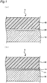
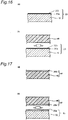
- Fig. 1(a) is a schematic cross-sectional view of a copper alloy article 3 according to Embodiment 1.
- the copper alloy article 3 includes a copper alloy substrate 10, a polyester-based resin substrate 40, and a compound layer 20 disposed therebetween.
- the copper alloy substrate 10 and the polyester-based resin substrate 40 are bonded via the compound layer 20.
- Fig. 1(b) is a schematic cross-sectional view of the copper alloy article 3 in which two compound layers exist between the copper alloy substrate 10 and the polyester-based resin substrate 40.
- the compound layer includes a first compound layer 20a and a second compound layer 20b.
- the copper alloy substrate 10 is made of pure copper or various copper alloys, and any copper alloy which is industrially used can be used as the copper alloy.
- a copper foil such as an electrolytic copper foil or a rolled copper foil can be applied.
- a rolled copper foil having high flexibility is suitable for FPC.
- the polyester-based resin substrate 40 is made of a polyester-based resin.
- the polyester-based resin is, for example, a polycondensate of a polyvalent carboxylic acid (dicarboxylic acid) and a polyalcohol (diol).
- Polyethylene terephthalate (PET) polymethylene terephthalate, polybutylene terephthalate, polyethylene naphthalate, polybutylene naphthalate, and a liquid crystal polymer (LCP) are preferred.
- polyester-based resin substrate 40 for example, a polyester-based resin film, a polyester-based resin plate, or the like can be used.
- an LCP film has a material characteristic of a low dielectric constant and a low dielectric loss tangent, when applied to FPC, there is an advantage that particularly a transmission loss of a high-frequency signal line is reduced. Further, the LCP film has a very low water absorption, and thus has good dimensional stability even under high humidity.
- a copper alloy article using a rolled copper foil as the copper alloy substrate 10 and an LCP film as the polyester-based resin substrate will be described in detail. It should be noted that the copper alloy article 3 using the copper alloy substrate 10 and the polyester-based resin substrate 40 of other forms can be also similarly configured and manufactured.
- the surface of the copper alloy substrate 10 is preferably flat, and for example, the surface roughness Ra is preferably 0.1 ⁇ m or less.
- the surface roughnesses Ra and R z can be measured by a contact surface roughness meter, a laser microscope, or the like.
- it is preferred that the copper alloy is exposed to the surface of the copper alloy substrate 10. Therefore, a method of selecting a copper alloy substrate 10 suitable for any of the embodiments will be examined.
- Copper foils A to C three types of commercially available copper foils (copper foils A to C) were selected for a copper foil having a thickness of 18 ⁇ m, which is the most demanded in FPC, and the surface layer was measured by X-ray photoelectron spectroscopy (XPS).
- XPS X-ray photoelectron spectroscopy
- Copper foil A was used for existing FPC, but zinc was detected from XPS measurement. That is, it was found that the copper foil A was zinc-plated.
- a copper foil suitable for Embodiment 2 a copper foil without a plating layer is preferred, and thus the copper foil A was excluded.
- the surface roughness Ra was measured with a laser microscope.
- the copper foil B had R a of 0.05 ⁇ m, and the copper foil C had R a of 0.15 ⁇ m.
- the copper foil B had fewer oil spots than the copper foil C.
- a commercially available copper foil is coated with a rust inhibitor. Further, an oxide layer can be produced on the surface of the copper foil over time.
- copper alloy articles such as FCP
- FCP in order to maximize the properties of the copper foil, for example, electrical conductivity, it is desirable to remove the rust inhibitor and the oxide layer from the surface of the copper foil and to expose the copper to the surface of the copper foil.
- cleaning acid cleaning
- a cleaning solution 15% sulfuric acid and 1% hydrochloric acid at room temperature were used. After the sample was immersed in the cleaning solution for 0 minute (no cleaning), 1 minute, and 5 minutes, the sample was taken out of the cleaning solution, sufficiently cleaned with ion-exchanged water, and dried. Thereafter, the surface of the sample was subjected to XPS analysis to determine a cleaning level.
- the cleaning level of the surface of the copper foil after acid cleaning was determined by whether or not a rust inhibitor remained on the surface.
- the surface of the copper foil after cleaning was measured by XPS, and qualitatively determined by the presence or absence of a nitrogen (N) peak (peak of a nitrogen N 1s orbital near a binding energy of 400 eV) derived from the rust inhibitor.
- N nitrogen
- Table 2 shows the measurement results.
- the oxide layer may be also used as a criterion for determining the cleaning level.
- the oxide layer could be completely removed from the surface of the copper foil by acid cleaning, at the moment when the copper foil was taken out of the cleaning solution, the copper on the surface of the copper foil reacted with oxygen in the atmosphere and a trace amount of oxide was produced.
- the surface analysis by XPS since even such a trace amount of oxide is detected, it is difficult to accurately determine the cleaning level.
- the peak derived from the N 1s orbital and the peak derived from the Cu 2p orbital were confirmed, from which it can be seen that the acid-cleaned copper foil was used.
- the absence of the rust inhibitor can be confirmed by the absence of the peak derived from the N 1s orbital.
- the peak derived from the Cu 2p orbital is very small (for example, the peak intensity of 1/10 or less, especially the peak intensity of 1/20 or less with respect to the peak intensity of the peak derived from Cu-O present in the vicinity of 935 eV), the absence of the oxide layer can be confirmed.
- the copper foil is then taken out to the atmosphere to form a small amount of oxide.
- the copper foil since such a very small amount of oxides do not have substantial influence on the characteristics of the copper foil (particularly, the bonding strength with the polyester-based resin substrate), it can be considered that there is substantially no oxide layer.
- a compound layer 20 includes two types of compounds, a first compound having a nitrogen-containing functional group and a silanol group, and a second compound which is an alkane-type amine-based silane coupling agent. Any of them can be used alone as a silane coupling agent, but in the embodiment of the present invention, it has been found that a bulky first compound and a linear second compound are used in combination, thereby increasing the bonding strength as compared with the case in which the compounds are used alone.
- the nitrogen-containing functional group Since the nitrogen-containing functional group has high chemical adsorbability to copper, it is effective in increasing the bonding strength to the copper alloy substrate 10. Since the silanol group has high chemical adsorbability to the ester structure of the polyester-based resin, it is effective in increasing the bonding strength to the polyester-based resin substrate 40. Therefore, a compound having a nitrogen-containing functional group and a silanol group (first compound) is suitable for bonding the copper alloy substrate 10 and the polyester-based resin substrate 40.
- the present inventors first discovered that by coexistence of a linear silane coupling agent (second compound) with to the first compound as described above, the bonding strength between the copper alloy substrate 10 and the polyester-based resin substrate 40 can be increased. The reason why such an effect is obtained is not clear, but it is considered to be due to the following mechanism.
- the second compound which is an alkane-type amine-based silane coupling agent has a relatively low bulk structure (for example, a linear structure).
- the first compound having a nitrogen-containing functional group and a silanol group has a bulky structure as compared with a linear second compound. Therefore, in a situation in which only the first compound is present, the first compounds are unlikely to approach each other. Since the second compound can enter between the bulky first compounds, the density of the compound in the compound layer 20 can be increased. Accordingly, when the polyester-based resin substrate 40 and the copper alloy substrate 10 are bonded via the compound layer 20, the bonding strength can be increased.
- the bonding strength between the copper alloy substrate 10 and the polyester-based resin substrate 40 can be improved.
- the copper alloy substrate 10 and the polyester-based resin substrate 40 can be firmly bonded, without roughening the surfaces of the copper alloy substrate 10 and the polyester-based resin substrate 40 and forming the metal oxide layer on the surface of the copper alloy substrate.
- the "nitrogen-containing functional group" of the first compound preferably has a 5 or more-membered ring structure containing nitrogen.
- the 5 or more-membered ring structure containing nitrogen can be, for example, a triazole or triazine structure.
- the structure of the first compound particularly becomes bulky, so that the first compounds are less likely to approach each other, and thus, the effect of improving the bonding strength is further pronounced by mixing the second compound with the first compound.
- the compound layer includes the first compound and the second compound can be confirmed by an analysis method such as XPS analysis.
- an analysis method such as XPS analysis.
- XPS analysis for example, in the spectrum obtained by XPS analysis of the compound layer, within the range of the binding energy at which the N 1s peak appears, a peak attributed to a nitrogen atom bonded by a double bond, a peak attributed to a nitrogen atom of a primary amino group, a peak attributed to a nitrogen atom of a secondary amino group, and the like are included.
- Those peaks can be identified by an analysis spectrum of the XPS spectrum.
- the nitrogen atom contained in the first compound and the nitrogen atom contained in the second compound are in different bonding states, the peaks of the XPS spectrum attributed to those nitrogen atoms can be identified. Thus, it can be specified that the first compound and the second compound are included in the compound layer.
- each compound is referred to by the symbol shown in Table 3).
- the chemical name of a compound is indicated when it is disclosed, but for the compound ImS of which the details are not disclosed, the disclosed basic structure is described.
- the main functional groups of these compounds are shown in Table 4. It is known that an alkoxysilane group becomes a silanol group in an aqueous solution. Among them, only the compound ET does not have an alkoxysilane group and is not a silane coupling agent.
- KBM-603 AS 3-aminopropyltrimethoxysilane Shin-Etsu Chemical Co., Ltd. KBM-903 [Table 4] Symbol Compound Main functional group ET 1,3,5-tris-(2,3-epoxypentyl)-1,3,5-triazin-2,4,6-(1 H ,3 H ,5 H )trione
- Basic structure triazine 6-membered ring epoxy group oxo group AST 2-(3-triethoxysilylpropyl) amino-4,6-di(2-aminoethyl)amino-1,3,5-triazine
- Basic structure triazine 6-membered ring alkoxysilane group amino group ImS Imidazole-based silane compound
- Basic structure imidazole 5-membered ring alkoxysilane group AAS N-2(aminoethyl)-3-aminopropyltrimethoxysilane
- Basic structure alkane alkoxy
- the ET-coated copper foil no peak indicating chemical adsorption between copper (Cu) and N atoms appeared.
- ET-coated LCP and PET no chemical shift of the peak indicating chemical adsorption with the epoxy group occurred. From these results, it was shown that ET was not chemically adsorbed on any surface of copper foil, LCP, and PET, but was only physically adsorbed thereon.
- a compound AST is a compound having a nitrogen-containing functional group and a silanol group (that is, the first compound), and the compound AST has one alkoxysilane group and two amino groups on a triazine 6-membered ring containing three nitrogen atoms.
- the copper foil coated with AST from a Cu 2p orbital peak of copper, a peak indicating a bond between Cu and N was confirmed.
- a compound ImS is a compound having a nitrogen-containing functional group and a silanol group (that is, a first compound), and has a structure in which a 5-membered imidazole ring and one alkoxysilane group are connected.
- a Cu 2p orbital peak of copper shows that there is a peak indicating a bond between Cu and N, and the imidazole group is chemically adsorbed on copper.
- the AST no Cu (0 valent) peak was observed, showing that AST was chemically adsorbed on the copper surface with a higher density than ImS was.
- Compounds AAS and AS are alkane-type amine-based silane coupling agents (that is, the second compounds), and are typical compounds which are widely applied to adhesion of copper and a resin in the prior art documents.
- the copper foil coated with these compounds it was shown from a Cu 2p orbital peak of copper that there was a peak of Cu (0 valent) like ImS, and there was a portion of the copper surface on which AAS or AS was not adsorbed. That is, it has been described in many documents that a silanol group is chemically adsorbed on a copper surface, but unlike the documents, it was found that the chemical adsorbability of these compounds was lowered on a sufficiently acid-cleaned copper surface.
- the substituent of a nitrogen-containing cyclic compound may be a ureido group, an isocyanate group, or the like, in addition to the amino group of AST.
- aqueous solution containing a predetermined compound was applied to an LCP film, which was then heat-treated at 100°C for 5 minutes.
- XPS analysis was performed on the film of the compound formed on the LCP film surface.
- Fig. 2 shows the N 1s peak of the XPS spectrum of the ImS film, which is separated into two spectra by an XPS spectrum analysis software.
- the second peak appearing at the position of a binding energy of 398.99 eV is assigned to the amino-type nitrogen atom (labeled as ">N-" in Fig. 2 ) contained in the 5-membered imidazole ring.
- the second peak intensity is almost the same as the first peak intensity.
- Fig. 3 shows the N 1s peak of the XPS spectrum of the AAS film, which is separated into three spectra by the analysis software.
- the peak appearing at the position of a binding energy of 399.98 eV is assigned to the nitrogen atom of the primary amino group (labeled as "-NH 2 " in Fig. 3 ).
- the peak appearing at the position of a binding energy of 399.12 eV is assigned to the nitrogen atom of the secondary amino group (labeled as "-NH" in Fig. 3 ).
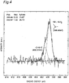
- Fig. 4 shows the N 1s peak of the XPS spectrum of the film of the compound containing ImS and AAS, which is separated into two spectra by the analysis software.
- the presence of this peak indicates that the measured film of the compound contains ImS.
- the second peak appearing at the position of a binding energy of 399.44 eV is formed by overlap of a peak attributed to the amino-type nitrogen atom (labeled as ">N-" in Fig. 4 ), a peak attributed to the nitrogen atom of the primary amino group (labeled as "-NH 2 "), and a peak attributed to the nitrogen atom of the secondary amino group (labeled as "-NH”).
- the second peak intensity is about 2.5 times the first peak intensity.
- the intensity of the second peak is significantly increased with respect to the first peak, and thus, it can be seen that a compound containing an amino group (AAS in this example) in addition to ImS is included in the film of the compound.
- a solution containing the first compound having a nitrogen-containing functional group and a silanol group and the second compound which is an alkane-type amine-based silane coupling agent was brought into contact with the surface of a polyester-based resin substrate 40.
- the solution can be brought into contact with the surface of the polyester-based resin substrate 40 by a known method such as coating or spraying.
- the compound layer 20 can be formed on the surface of the polyester-based resin substrate 40 ( Fig. 5(a) ).
- a polyester-based resin member 47 including the polyester-based resin substrate 40 and the compound layer 20 is obtained.
- a first solution containing the first compound and a second solution containing the second compound may be separately prepared.
- the first compound and the second compound can be mixed and adsorbed on the surface of the polyester-based resin substrate 40.
- the second solution may be brought into contact after the first solution is brought into contact, or the second solution may be brought into contact after the second solution is brought into contact.
- the nitrogen-containing functional group has a 5 or more-membered ring structure containing nitrogen.
- the 5 or more-membered ring structure is a triazole or triazine structure.
- Specific examples of the compound include AST, ImS, an AST-like compound in which some of the functional groups of AST are replaced with other functional groups, and an imidazole silane coupling agent, and the like, described in Table 5.
- Examples of the AST-like compound include a compound in which the triethoxy group of AST is a trimethoxy group, and a compound in which the amino substituent of the 4,6-di(2-aminoethyl) amino group of AST is an N-2-(aminoethyl)-3-aminopropyl group, a 3-aminopropyl group, an N-(1,3-dimethyl-methylidene)propylamino group, an N-phenyl-3-aminopropyl group, an N-(vinylbenzyl)-2-aminoethyl-3-aminopropyl group, or a 3-ureidopropyl group.
- imidazole silane coupling agent examples include those having tris-(trimethoxysilylpropyl) isocyanurate, any one of a 1-imidazolyl group, a 3-imidazolyl group, and a 4-imidazolyl group, and a trialkoxysilyl group such as a trimethoxy group and a triethoxy group, together.
- alkane-type amine-based silane coupling agent a linear alkane-type amine-based silane coupling agent is preferred.
- the compound include N-2-(aminoethyl)-3-aminopropylmethyldimethoxysilane, N- 2 - (aminoethyl) - 3 - aminopropyltrimethoxysilane, 3-aminopropyltrimethoxysilane, 3-aminopropyltriethoxysilane, and the like.
- the surface of the copper alloy substrate 10 is cleaned with an acid aqueous solution. This allows the oxide layer and the rust inhibitor present on the surface of the copper alloy substrate 10 to be removed.
- an aqueous solution of an acid solution such as sulfuric acid, hydrochloric acid, a mixed solution of sulfuric acid and chromic acid, a mixed solution of sulfuric acid and hydrochloric acid, and a mixed solution of sulfuric acid and nitric acid can be used.
- an acid solution such as sulfuric acid, hydrochloric acid, a mixed solution of sulfuric acid and chromic acid, a mixed solution of sulfuric acid and hydrochloric acid, and a mixed solution of sulfuric acid and nitric acid
- a sulfuric acid aqueous solution or a hydrochloric acid aqueous solution is preferred.
- the cleaning can be performed by immersing the copper alloy substrate 10 in an acid aqueous solution for a predetermined time.
- the immersion time may be only within a range which allows removal of the oxide layer and the rust inhibitor on the surface and does not significantly erode the copper alloy substrate 10. For example, when 1% hydrochloric acid is used, immersion can be performed for 30 seconds to 10 minutes (for example, 1 minute). When 15% sulfuric acid is used, immersion may be performed for 1 to 20 minutes (for example, 5 minutes).
- the compound layer 20 of the polyester-based resin member 47 and the cleaned copper alloy substrate 10 are brought into contact with each other and pressed to bond the polyester-based resin member 47 and the copper alloy substrate 10, thereby obtaining the copper alloy article 3 as shown in Fig. 1 .
- This can be regarded as bonding the polyester resin substrate 40 of the polyester-based resin member 47 and the copper alloy substrate 10 via the compound layer 20.
- the heating temperature is set to a temperature at which the polyester-based resin substrate 10 of the polyester-based resin member 47 does not melt. Pressing can be performed at a surface pressure of 1 MPa to 8 MPa, for example, 4 MPa.
- the compound layer 20 may be formed on the surface of the copper alloy substrate 10.
- the modification example will be described with reference to Figs. 6(a) and 6(b) .
- a solution containing a compound having a nitrogen-containing functional group and a silanol group is brought into contact with the surface of the cleaned copper alloy substrate 10. Thereafter, a heat treatment can be performed to form the compound layer 20 on the surface of the copper alloy substrate 10 ( Fig. 6(a) ). Thus, a copper alloy member 15 including the copper alloy substrate 10 and the compound layer 20 is obtained.
- the surface of the copper alloy substrate 10 is cleaned with an acid aqueous solution to remove the oxide layer and the rust inhibitor present on the surface of copper alloy substrate 10, in the same manner as in Step 1-2. of Embodiment 1.
- the polyester-based resin substrate 40 and the compound layer 20 of the copper alloy member 15 are brought into contact with each other and pressed to bond the polyester-based resin substrate 40 and the copper alloy member 15, thereby obtaining the copper alloy article 3 as shown in Fig. 1 .
- the polyester-based resin member 47 including the compound layer 20 ( Fig. 5(a) ) and the copper alloy member 15 including the compound layer 20 ( Fig. 6(a) ) are prepared, and the compound layers 20 are brought into contact with each other and pressed, thereby obtaining the copper alloy article 3 as shown in Fig. 1 .
- the compound layer of the polyester-based resin member 47 may be formed from the first solution containing the first compound having a nitrogen-containing functional group and a silanol group
- the compound layer of the copper alloy member 15 may be formed from the second solution containing the second compound which is an alkane-type amine-based silane coupling agent.
- the effect of improving the bonding strength may not be sufficiently exhibited, and thus, it is preferred to appropriately select a method of forming a compound layer, depending on the compound to be used.
- LCP film pieces Four specimens (LCP film pieces) were prepared by cutting an LCP film CT-Z (manufactured by KURARAY CO., LTD.) having a thickness of 50 ⁇ m into a square having a side of 150 mm. Any one of four types of compound aqueous solutions (ET aqueous solution, AAS aqueous solution, ImS aqueous solution, and AST aqueous solution) was applied to both surfaces of the specimen of the LCP film, using a dip coater manufactured by JSP Corporation. The concentration of each aqueous solution was 0.1%.
- a copper foil B (manufactured by UACJ corporation, thickness of 18 ⁇ m) was cleaned with 1% hydrochloric acid for 1 minute, then sufficiently washed with ion-exchanged water, and dried. Thereafter, eight specimens (copper foil pieces) obtained by cutting the copper foil B into 150 mm squares were also prepared. Then, any one of the above-described four types of compound aqueous solutions was applied to both surfaces of the copper foil specimen, using a dip coater manufactured by JSP Corporation. In addition, one type of compound aqueous solution was applied to two pieces of copper foil.
- the LCP film piece and the copper foil piece to which the aqueous solution was applied were heat-treated at 100°C for 5 minutes.
- compound layers were formed on both surfaces of the LCP film piece and both surfaces of the copper foil piece.
- the copper foil pieces were placed on both surfaces of the LCP film piece on which the compound layer was formed, and while pressing at a surface thickness of 4 MPa with a vacuum press manufactured by KITAGAWA SEIKI Co., Ltd., the temperature was raised to 270°C, maintained for 20 minutes, and then kept at 290°C for 10 minutes, thereby preparing a double-sided copper-clad laminate.
- a compound layer is placed between the LCP film and the copper foil.
- the compound aqueous solution was applied to both the LCP film and the copper foil, but even in the case in which the compound aqueous solution is applied to either one, the compound layer can be formed between the LCP film and the copper foil. That is, the surface to be applied can be appropriately determined, depending on the wettability of the compound solution, the easiness of forming the compound layer, the required amount of the compound, and the like.
- a double-sided copper-clad laminate was prepared in the same manner, using a specimen in which neither of the LCP film and the copper foil was coated with the compound aqueous solution.
- a specimen in a strip shape was cut out from the double-sided copper-clad laminate, the entire surface of the copper foil on the rear was removed by etching according to JIS C 6471, Section 8.1, "Peel-off strength of copper foil", and a 10 mm wide pattern remained on the test surface by etching, thereby preparing a peel test specimen.
- the LCP film side on the rear of the peel test specimen was fixed to a reinforcing plate with double-sided tape, the copper foil was peeled off in a 180° direction at a peel speed of 50 mm/min, using Autograph AGS-5 kNX manufactured by Shimadzu Corporation, and a peel strength was measured for three pieces at one time under each condition. The minimum and maximum values were read from the peel test chart.
- the LCP film and the copper foil were not bonded, and peeling off occurred at the interface between the copper foil and the LCP film.
- the minimum and maximum values of the peel strength were 0.16 kN/m and 0.20 kN/m, respectively.
- first compound a compound having a nitrogen atom-containing cyclic molecular structure
- second compound an alkane-type amine-based silane coupling agent
- a specimen (LCP film piece) was prepared by cutting an LCP film CT-Z (manufactured by KURARAY CO., LTD.) having a thickness of 50 ⁇ m into a square having a side of 150 mm.
- Four LCP film pieces were prepared.
- One of the compound aqueous solutions including the compound of Table 7 was applied to both surfaces of the LCP film piece, using a dip coater manufactured by JSP Corporation.
- the compound layer was formed using a mixed aqueous solution containing 0.1% by weight of ImS and 1% by weight of AAS.
- Comparative Example 1 an aqueous solution containing 0.1% by weight of ImS was used, and in Comparative Example 2, an aqueous solution containing 0.1% by weight of AAS was used.
- a "copper foil B" (manufactured by UACJ corporation, thickness of 18 ⁇ m) shown in Table 1 was cleaned with 1% hydrochloric acid for 1 minute, then sufficiently washed with ion-exchanged water, and dried. Thereafter, a specimen (copper foil piece) obtained by cutting the copper foil B into 150 mm squares was prepared. Eight copper foil pieces were prepared. Then, any one of the above-described four types of compound aqueous solutions was applied to both surfaces of the copper foil piece, using a dip coater manufactured by JSP Corporation. In addition, one type of compound aqueous solution was applied to two pieces of copper foil.
- the LCP film piece and the copper foil piece to which the aqueous solution was applied were heat-treated at 100°C for 5 minutes.
- compound layers were formed on both surfaces of the LCP film piece and both surfaces of the copper foil piece.
- the copper foil pieces were placed on both surfaces of the LCP film piece on which the compound layer was formed, and while pressing at a surface thickness of 4 MPa with a vacuum press manufactured by KITAGAWA SEIKI Co., Ltd., the temperature was raised to 270°C, maintained for 20 minutes, and then kept at 290°C for 10 minutes, thereby preparing a double-sided copper-clad laminate.
- a compound layer is placed between the LCP film and the copper foil.
- Table 7 shows the results of the peel test.
- Compound Peel strength (kN/m) (Minimum value/maximum value) Peeled state
- Comparative Example 2 AAS 0.32/0.37 Thin cohesive peeling
- Example 1 when the LCP film and the copper foil were bonded by a compound layer including the compound ImS (first compound) and the compound AAS (second compound) in combination, the minimum and maximum values of the peel strength were 0.44 kN/m and 0.68 kN/m, respectively.
- the peel strength of Example 1 was about 1.55 times the peel strength of Comparative Example 1 (0.68/0.44), and about 1.84 times the peel strength of Comparative Example 2 (0.68/0.37). In other words, it was found that the peel strength can be improved by 1.5 times or more as compared with the case of using each compound alone, only by mixing the compound ImS and the compound AAS as in Example 1. By comparing the maximum values, it is possible to know how much the maximum value of the bonding strength which can be realized by the compound layer as in Example 1 can be improved.
- Example 2 a specimen ("double-sided copper-clad laminate" in which an LCP film piece and a copper foil piece were laminated) was prepared in the same manner as in Example 1, using a compound aqueous solution containing the compound of Table 8, and a peel test was performed. Specifically, in Example 2, the compound layer was formed using a mixed aqueous solution containing 0.1% by weight of AST and 1% by weight of AAS. In Comparative Example 3, an aqueous solution containing 0.1% by weight of AST was used.
- Table 8 shows the results of the peel test.
- Compound Peel strength (kN/m) (Minim um value/maximum value) Peeled state
- Example 2 when the LCP film and the copper foil were bonded by a compound layer including the compound AST (first compound) and the compound AAS (second compound) in combination, the minimum and maximum values of the peel strength were 0.68 kN/m and 0.77 kN/m, respectively.
- the peel strength of Example 2 was about 2.08 times the peel strength of Comparative Example 2 (0.77/0.37), and about 1.13 times the peel strength of Comparative Example 3 (0.77/0.68). In other words, it was found that the peel strength can be improved by 1.13 times or more as compared with the case of using each compound alone, only by mixing the compound AST and the compound AAS as in Example 2.
- the bonding strength by using AST alone is sufficiently high among conventional silane coupling agents, but according to the embodiment of the present invention, the bonding strength can be further improved.
- the mechanism of micro-chemical adsorption is estimated. Since the first compound having a cyclic molecular structure containing a nitrogen atom (for example, the compounds ImS and AST) has a large molecular structure, there occurs a gap between molecules during chemical adsorption. A second compound having a low molecular weight and a chain structure (for example, the compound AAS) has the effect of entering the gap between the molecules of the first compounds ImS and AST and closing the gap. Thus, it is considered that the chemical adsorption density of a total of the first compound and the second compound can be increased, and as a result, the bonding strength between the LCP film and the copper foil can be improved.
- the first compound having a cyclic molecular structure containing a nitrogen atom for example, the compounds ImS and AST
- AAS the compound having a low molecular weight and a chain structure
- the total molar concentration of AST and AAS was fixed at 48 mmol/L, and the concentration of AST and AAS was changed from 1 : 0 to 1 : 15 as a molar ratio (from 2 : 0 to approximately 0.1 : 1.0 as a % by weight ratio).
- the reason why the molar concentration was constant is that the characteristics of the compounds can be correctly compared by comparing the number of molecules in the solution. That is, the relation between the chemical adsorbability of each molecule and the bonding strength can be correctly compared, by specifying in the molar concentration.
- a specimen (double-sided copper-clad laminate) used in the peel test was formed in the same manner as in Example 1.
- the minimum and maximum values of the peel strength were 0.60 kN/m and 0.65 kN/m, respectively.
- the peel strength tends to be improved.
- the minimum value of the peel strength is 0.63 to 0.70 kN/m, and the maximum value thereof is 0.67 to 0.73 kN/m.
- the maximum value of the peel strength was about 1.12 times that of Comparative Example 4 (0.73/0.65).
- the minimum and maximum values of the peel strength of Example 7 were 0.55 kN/m and 0.61 kN/m, respectively, which were lower than those of Comparative Example 4, but were higher than the peel strength (the minimum value of 0.42 kN/m and the maximum value of 0.47 kN/m) of Comparative Example 5 (using an aqueous solution containing only AAS).
- the molar ratio of the first compound (AST) : the second compound (AAS) is 1 : 1 to 1 : 10 (Examples 4 to 6)
- the maximum value of a tensile strength of 0.70 kN/m or more, which could not be achieved with the conventional compound, can achieve an extremely strong bonding strength.
- a mixed aqueous solution containing the first compound (compound AST) and the second compound (compound AAS) was applied to the surface of the copper foil piece.
- the mixed aqueous solutions to be used are the same as those used in Examples 3 to 6 and Comparative Examples 4 to 5 (see Table 9).
- any one of the aqueous solutions is applied to the surface (both surfaces) of the copper foil piece, using a dip coater manufactured by JSP Corporation. Thereafter, the copper foil piece was heat-treated at 100°C for 5 minutes to form a compound layer on the surface of the copper foil piece, and the surface of the copper foil piece coated with the compound layer was subjected to XPS analysis. XPS spectrum of each copper foil piece is shown in Figs. 7 to 12 .
- the XPS spectrum was analyzed focusing on the Cu 2p orbital peak of the XPS spectrum.
- a Cu-N bond peak, a Cu-O bond peak, and a Cu (0 valent) peak are mainly observed.
- the Cu-N bond peak is labeled as "Cu-N”
- the Cu-O bond peak is labeled as "Cu-O”
- the Cu (0 valent) peak is labeled as "Cu (0)”.
- Fig. 7 is an XPS spectrum of a copper foil piece having a compound layer formed by the AST aqueous solution (see Table 9) used in Comparative Example 4.
- Table 9 a slightly smaller Cu-O bond peak was observed in addition to the main Cu-N bond peak (Table 5).
- the Cu (0 valent) peak was not observed behind the noise.
- the silanol group shown by the Cu-O bond peak is a functional group contributing to chemical adsorption with an ester structure contained in LCP, PET, and the like. Therefore, in order to improve the peel strength of the copper foil and the resin film having an ester structure, it is considered to be preferred that the ratio of the silanol groups chemically adsorbed on the surface of the copper foil (that is, the consumed silanol groups) is small. That is, it is preferred that no Cu-O bond peak is observed (or the peak is as small as possible) in the XPS spectrum.
- Fig. 8 is an XPS spectrum of the copper foil piece having a compound layer formed by the AAS aqueous solution (see Table 9) used in Comparative Example 5.
- the peak of the Cu 2p orbital in the XPS spectrum of Fig. 8 is analyzed in detail, similarly to the XPS spectrum of Fig. 7 (AST coating), Cu (0 valent) peak was also observed, in addition to the Cu-N bond peak and the rather small Cu-O bond peak, as in the XPS spectrum (coated with AST) of Fig. 7 .
- Figs. 9 to 11 are XPS spectra of copper foil pieces having a compound layer formed by a mixed aqueous solution of AST and AAS (see Table 9) used in Examples 3 to 5.
- the molar ratio of AST and AAS in the mixed aqueous solution to be used is 1 : 0.5
- the molar ratio is 1 : 1
- the molar ratio is 1 : 2.
- the peak intensities of the Cu-O bond peak and Cu (0 valent) peak are larger than those of Figs. 7 and 8 , and are close to the peak intensity of the Cu-N bond peak. That is, by mixing AAS with AST, a Cu (0 valent) peak, which was not observed in Fig. 7 (AST alone), was observed, and the peak intensity of the Cu-O bond peak was increased to the same level as the Cu-N bond peak.
- Fig. 12 is an XPS spectrum of a copper foil piece having a compound layer formed by a mixed aqueous solution of AST and AAS (see Table 9) used in Example 6.
- the molar ratio of AST to AAS in the mixed aqueous solution used is 1 : 10.
- the ratio of AAS is high, the effect of mixing AST and AAS cannot be obtained.
- the ratio of AAS in the mixed aqueous solution was too high (the molar ratio AST and AAS was 1 : 15) in Example 7, the peel strength was significantly decreased. In the embodiment, it is considered that the effect of AAS is the main.
- a compound layer having a high bonding strength can be formed by mixing the first compound having a bulky cyclic structure and the second compound having a linear structure. Furthermore, it was confirmed that by appropriately adjusting the mixing ratio of these compounds, it is possible to particularly effectively use the difference in the three-dimensional structure between the compound having a bulky cyclic structure and the compound having a linear structure, and the density and structure of the chemical adsorption of the compound to the copper foil and the resin film having an ester structure can be optimized.
- the specimens (double-sided copper-clad laminates) of Comparative Examples 4 to 5 and Example 6 were prepared in the same manner as in the above "(A) Peel test".
- the obtained copper-clad laminate was immersed in a 30 to 35% ferric chloride aqueous solution at a temperature of 60°C for 5 to 6 minutes to dissolve and remove the copper foil (wet etching).
- the compound layer formed between the copper foil and the LPC film piece was exposed.
- the specimen was washed with ion-exchanged water and dried in an oven at 80°C for 30 minutes to obtain an LPC specimen for FT-IR analysis (an LPC film piece coated with a compound layer).
- FT-IR analysis For the LPC specimen for measurement, the surface coated with the compound layer was subjected to FT-IR analysis.
- FT-IR analysis a Fourier transform infrared spectrophotometer FT/IR680 Plus manufactured by JASCO Corporation equipped with a multiple total reflection measuring device ATR500/M manufactured by JASCO Corporation was used, and measurement was performed by an attenuated total reflection (ATR) method.
- ATR attenuated total reflection
- a Ge prism was used and measuring was performed with 5 reflections at an incident angle of 45°.
- FT-IR charts of each LPC specimen are shown in Figs. 13 to 15 .
- Fig. 13 is an FT-IR chart of an LPC specimen prepared from the copper-clad laminate of Comparative Example 4.
- Fig. 14 is an FT-IR chart of an LPC specimen prepared from the copper-clad laminate of Comparative Example 5.
- Fig. 15 is an FT-IR chart of an LPC specimen prepared from a copper-clad laminate of Example 6.
- the FT-IR chart of Fig. 15 is significantly different from those in Figs. 13 and 14 .
- a peak of a C-N group of a triazine ring of AST at 3295 cm -1 and peaks of a CH 2 group at 2966 cm -1 and 2926 cm -1 are stronger than those in Figs. 13 and 14 .
- a peak of a Si-OH group was detected at 920 cm -1 , as in Figs. 13 and 14 .
- the copper metal substrate and the polyester-based resin member were able to be strongly bonded, by adding the alkane-type amine-based silane coupling agent to the compound having a cyclic molecular structure containing a nitrogen atom in combination.
- the structure containing nitrogen of the second compound and the first compound was chemically adsorbed in a large amount on the metal substrate, and the structure of Si-OH containing no nitrogen was chemically adsorbed in a large amount on the resin substrate. That is, it is understood that in a member in which the first compound layer is formed on the metal substrate, the structure containing nitrogen is chemically adsorbed to the metal substrate, and there are many Si-OH structures on the surface of the first compound layer of the member.
- the effectiveness of the first compound layer has been clarified, but in order to further improve the bonding strength, it is considered that a compound having a structure in which a Si-OH functional group having excellent chemical adsorbability to the resin substrate is contained, and simultaneously, other Si-OH functional groups on the surface of the resin substrate form a chemical bond with a Si-OH group which are present in a large amount in the first compound layer on the surface of the metal member, is applied, and in addition to the first compound layer composed of the first compound and the second compound, the second compound layer composed of the third compound which is a silane compound having two or more of alkoxysilyl groups or silanol groups is interposed between the metal substrate and the resin substrate, thereby further improving the bonding strength, and the present invention has been reached.
- a polyimide film manufactured by a conventionally known method can be used as the polyimide film applied to the base material for a flexible printed circuit board in Embodiment 2 of the present invention. That is, a film obtained by forming a polyamic acid obtained by a reaction between tetracarboxylic dianhydride and an aromatic diamine into a film and thermally or chemically imidizing the film can be used.
- the thickness and surface roughness of the film are not particularly limited, but it is preferred that the thickness is in a range of 10 to 100 ⁇ m and Rz is in a range of smaller than 200 nm.
- the film thickness is less than 10 ⁇ m, there is a concern about reliability such as an insulating property when fabricating a fine circuit, and when the film thickness is more than 100 ⁇ m, there is a concern that the moisture absorption and dimensional stability of the film may be reduced.
- the surface roughness of the film Rz is more than 200 nm, sufficient adhesion may not be obtained in bonding metals.
- the moisture absorption, the dimensional stability, and the like of the film can be appropriately selected depending on the application, but it is preferred that the moisture absorption is 1.0 wt% (23°C/50% RH) or less and the dimensional stability is 30 ppm (23°C, 0 to 70% RH) or less. Both are intended to maintain stability in the circuit forming process.
- a surface treatment such as a corona discharge treatment, a low-pressure plasma treatment, an atmospheric pressure plasma treatment, a flame treatment, and an ion bombardment treatment on at least one surface as a pretreatment.
- a corona discharge treatment is cost-effective.
- These surface treatments remove contamination on the polyimide film surface and uniformly form active functional groups on the surface.
- the wettability of the polyimide film after the surface treatment is preferably 73 dyne/cm or more.
- Prepreg applied to a base material for a printed circuit board is obtained by impregnating or coating a varnish of an insulating resin composition into or on a sheet or mat of an inorganic fiber such as glass, an organic fiber such as polyimide, polyester, and tetrafluoroethylene, and a mixture thereof, and is in a semi-cured state (B-stage state).
- the thickness of the prepreg layer varies depending on the application, but is preferably 0.1 to 5 mm.
- the resin used in the insulating resin composition a known insulating resin used as an insulating material for a printed circuit board can be used.
- thermosetting resin is used as a base due to the properties such as heat resistance and chemical resistance, and examples thereof include epoxy resins, phenol resins, cyanate resins, maleimide resins, isocyanate resins, benzocyclobutene resins, vinyl resins, and the like, but are not limited thereto.
- the thermosetting resin may be one type or a mixture of two or more types.
- the thermosetting resin includes a resin blended with a thermoplastic resin, from the necessity of dielectric properties, impact resistance, processability, and the like.
- the thermoplastic resin include a fluorine resin, a polyphenylene ether resin, a modified polyphenylene ether resin, a polyphenylene sulfide resin, a polycarbonate resin, a polyetherimide resin, a polyetheretherketone resin, a polyarylate resin, a polyamide resin, a polyamideimide resin, a polybutadiene resin, and the like, but are not limited thereto.
- the thermoplastic resin may be a single type or a mixture of two or more types.
- An inorganic filler may be mixed with the insulating resin composition.
- examples of the inorganic filler include alumina, aluminum hydroxide, magnesium hydroxide, clay, talc, antimony trioxide, antimony pentoxide, zinc oxide, fused silica, glass powder, quartz powder, shirasu balloon, and the like. These inorganic fillers may be used alone or as a mixture of two or more thereof.
- the insulating resin composition may contain an additive such as a flame retardant, a curing agent, a curing accelerator, thermoplastic resin particles, a coloring agent, an ultraviolet ray impermeable agent, an antioxidant, and a reducing agent, and a filler.
- an additive such as a flame retardant, a curing agent, a curing accelerator, thermoplastic resin particles, a coloring agent, an ultraviolet ray impermeable agent, an antioxidant, and a reducing agent, and a filler.
- polyamide-based and polyester-based resins which can be applied to the embodiment of the present invention are polyamide-based and polyester-based resins, and may have any form and shape such as a film material, a plate material, a bar material, a tube material, and a molding material.
- a polyamide-based (nylon) resin nylon 4, nylon 6, nylon 11, nylon 12, nylon 46, nylon 66, nylon 610, nylon MXD6 (polycondensate of meta-xylylenediamine and adipic acid), and the like, and copolymers thereof, and inorganic fillers, glass fibers, or carbon fibers may be added, and blends with other polymers may be also used.
- polyester-based resin polyethylene terephthalate, polymethylene terephthalate, polybutylene terephthalate, polyethylene naphthalate, polybutylene naphthalate, liquid crystal polymers, and the like, and copolymers thereof, and inorganic fillers, glass fibers, or carbon fibers may be added, and blends with other polymers may be also used.
- a metal which can be used in the embodiment of the present invention is copper and aluminum.
- the copper material pure copper, brass, bronze, white copper, nickel silver, cupronickel, beryllium copper, and the like can be used.
- the copper foil may be a rolled copper foil or an electrolytic copper foil.
- As the aluminum material any of 1000 series, 2000 series, 3000 series, 4000 series, 5000 series, 6000 series, 7000 series, and 8000 series can be used.
- As the aluminum foil 1N39, 1085, 1N90, 1N99, 3003, 3004, 8079, 8021, and the like can be used.
- the metal used in the embodiment of the present invention may be a metal which has been roughening-treated by an oxidation treatment, a reduction treatment, etching, and the like, but it is particularly preferred not to perform such a roughening treatment.
- the metal has a surface roughness Rz of preferably 1.5 ⁇ m or less, and more preferably 1.0 ⁇ m or less.
- the thickness of the metal is not particularly limited, but in the case of a metal foil, it is preferably 300 ⁇ m or less for practical use.
- At least the side of the metal in contact with the resin layer may be subjected to, for example, a surface treatment of any one of a rust prevention treatment and chromate treatment, or a combination of both. What surface treatment is performed can be appropriately selected depending on the resin.
- a solution containing the first compound having a nitrogen-containing functional group and a silanol group and the second compound which is an alkane-type amine-based silane coupling agent was brought into contact with the surface of a metal substrate 10. Thereafter, a heat treatment can be performed to form a first compound layer 20a. Further, if necessary, a solution containing a third compound which is a silane compound having two or more of alkoxysilyl groups or silanol groups was brought into contact with a surface of the first compound layer 20a, and thereafter, a heat treatment was performed to form a second compound layer 20b.
- the solution can be brought into contact with the surface of the metal substrate 10 by a known method such as coating or spraying.
- a metal member 15 including the compound layer 20a alone or both the compound layers 20a and 20b on the surface of the metal substrate 10 was obtained. ( Fig. 16(a) ).
- a solution containing a first compound having a nitrogen-containing functional group and a silanol group for forming a first compound layer and a second compound which is an alkane-type amine-based silane coupling agent, or a solution containing a third compound which is a silane compound having two or more of alkoxysilyl groups or silanol groups for forming a second compound layer was brought into contact with the surface of the resin substrate 40.
- the solution can be brought into contact with the surface of the resin substrate 40 by a known method such as coating or spraying.
- the compound layer 20b of either of the first compound layer or the second compound layer can be formed on the surface of the resin substrate 40 ( Fig. 17(a) ).
- a resin member 47 including the resin substrate 40 and the compound layer 20b is obtained.
- the resin substrate 40 and the compound layer 20a and/or the compound layer 20b formed on the metal base material 10 of the metal member 15 were brought into contact with each other and pressed to bond the resin base material 40 and the metal member 15, thereby obtaining the metal article 3 as shown in Fig. 1 .
- the compound layer 20b of either of the first compound layer or the second compound layer on the surface of the resin base material 40 of the resin member 47, and the compound layer of the compound layer 20a formed on the metal base material 10 of the metal member 15 were brought into contact with each other and pressed to bond the resin member 47 and the metal member 15, thereby obtaining the metal article 3 as shown in Fig. 1 .
- a specimen (LCP film piece) was prepared by cutting an LCP film CT-Z (manufactured by KURARAY CO., LTD.) having a thickness of 50 ⁇ m into a square having a side of 150 mm. Any one of a 0.05% aqueous solution of a polymer type polyfunctional group silane coupling agent forming a second compound layer (product name: X-12-972F, manufactured by Shin-Etsu Chemical Co., Ltd.), a melamine functional organosilicon compound (N,N,N-tris-(triethoxysilylpropyl) melamine, 0.03% ethanol solution), and an isocyanurate functional silicon compound (tris-(trimethoxysilylpropyl) isocyanurate, product name: KBM-9659, 0.02% isopropanol IPA solution) was applied to both surfaces of the specimen of the LCP film, using a dip coater manufactured by JSP Corporation.
- the LCP film piece and the copper foil piece to which each compound solution was applied were heat-treated at 100°C for 5 minutes.
- compound layers were formed on both surfaces of the LCP film piece and both surfaces of the copper foil piece.
- the copper foil pieces were placed on both surfaces of the LCP film piece on which the compound layer was formed, and while pressing at a surface thickness of 4 MPa with a vacuum press manufactured by KITAGAWA SEIKI Co., Ltd., the temperature was raised to 270°C, maintained for 20 minutes, and then kept at 290°C for 10 minutes, thereby preparing a double-sided copper-clad laminate.
- a vacuum press manufactured by KITAGAWA SEIKI Co., Ltd.
- a specimen in a strip shape was cut out from the double-sided copper-clad laminate, the entire surface of the copper foil on the rear was removed by etching according to JIS C 6471, Section 8.1, "Peel-off strength of copper foil", and a 10 mm wide pattern remained on the test surface by etching, thereby preparing a peel test specimen.
- the LCP film side on the rear of the peel test specimen was fixed to a reinforcing plate with double-sided tape, the copper foil was peeled off in a 90° direction at a peel speed of 50 mm/min, using Autograph AGS-5 kNX manufactured by Shimadzu Corporation, and the peel strength was measured for three pieces at one time under each condition. The minimum and maximum values were read from the peel test chart.
- Table 10 shows the results.
- the number of alkoxysilyl groups or silanol groups per a compound molecule used in the examples is large in the polymer type polyfunctional group silane coupling agent X-12-972F, three in the melamine functional organosilicon compound N,N,N-tris-(triethoxysilylpropyl) melamine, and three in the isocyanurate functional silicon compound KBM-9659.
- Table 10 shows that upon comparison with the minimum value of 0.70/ the maximum value of 0.73 kN/m of the peel test strength in the case of only the first compound layer of the mixed solution of AST and AAS of Example 6, the minimum value of 0.68/ maximum value of 0.72 kN/m of the second compound layer being the polymer type polyfunctional group silane coupling agent is almost equivalent, and both the minimum value of 0.75/ the maximum value of 0.82 kN/m of the melamine functional organosilicon compound and the minimum value of 0.78/ the maximum value of 1.24 kN/m of the isocyanurate functional silicon compound are higher than the peel strength of the mixed solution of AST and AAS.
- the bonding strength can be improved by forming a layer of a silane compound having two or more of alkoxysilyl groups or silanol groups on the polyester resin.
- a polymer type polyfunctional group silane coupling agent was selected.
- the effects of improving the peel strength of three types of compounds having different structures were compared, as shown in Table 10, and among them, the compound which had the result closest to the effect of improving the peel strength of the first compound layer composed of the first compound (AST) and the second compound (AAS) was the polymer type polyfunctional group silane coupling agent and had a somewhat small effect as compared with other types of compounds, but since it was determined that if this compound exhibited the effect, compounds having other structures also had the effect, the polymer type polyfunctional group silane coupling agent was selected in the present example.
- a polyimide film having a thickness of 50 ⁇ m (product name: Kapton 200EN, manufactured by DU PONT-TORAY CO., LTD.), a nylon film (product name: Emblem ON, manufactured by UNITIKA LTD.), and epoxy prepreg (product name: epoxy resin impregnated tape, manufactured by Teraoka Seisakusho Co., Ltd.) were used to prepare a specimen which was cut into a 150 mm square for each test.
- the polyimide film and the nylon film were corona discharge-treated as a pretreatment, and 0.1% normal propanol solution of a polymer type polyfunctional group silane coupling agent (product name: X-12-972F, manufactured by Shin-Etsu Chemical Co., Ltd.) was applied to both surfaces of the specimen of the film, using a dip coater manufactured by JSP Corporation. The compound solution was not applied to the surface of the prepreg.
- a polymer type polyfunctional group silane coupling agent product name: X-12-972F, manufactured by Shin-Etsu Chemical Co., Ltd.
- An aluminum foil manufactured by TOYO ALUMINIUM K.K., thickness of 50 ⁇ m was cut into a 150 mm square, immersed in a 3% aqueous solution of a degreasing solution (product name: GC26M, manufactured by MILLION CHEMICALS CO., LTD.) for 1 minute (60°C), and washed with water and dried to prepare a specimen. Then, a compound aqueous solution in which the first compound (AST) and the second compound (AAS) were mixed was applied to both surfaces of the specimen, in the same manner as the copper foil, using a dip coater manufactured by JSP Corporation.
- a degreasing solution product name: GC26M, manufactured by MILLION CHEMICALS CO., LTD.
- Example 14 The copper foil of Example 14 was coated with a mixed aqueous solution of the first compound (AST) and the second compound (AAS), heat-treated as described above, further coated with a 0.2% normal propanol solution of a polymer type polyfunctional group silane coupling agent (product Name: X-12-972F, manufactured by Shin-Etsu Chemical Co., Ltd.), and heat-treated at 100°C for 5 minutes.
- AST first compound
- AAS second compound
- a 0.2% normal propanol solution of a polymer type polyfunctional group silane coupling agent product Name: X-12-972F, manufactured by Shin-Etsu Chemical Co., Ltd.
- the copper foil piece was placed on both surfaces of the film piece on which the compound layer was formed, and in the case of the polyimide film, the copper foil piece was kept at 250°C for 10 minutes while being pressed at a surface thickness of 10 MPa with a vacuum press manufactured by KITAGAWA SEIKI Co., Ltd., thereby preparing a double-sided copper-clad laminate.
- Lamination was performed at a surface pressure of 4 MPa at 200°C for 90 minutes in the case of the prepreg, and at a surface pressure of 4 MPa at 200°C for 10 minutes in the case of a nylon film.
- each compound layer was placed between the film and the copper foil.
- a specimen in a strip shape was cut out from the double-sided copper-clad laminate, the entire surface of the copper foil on the rear was removed by etching according to JIS C 6471, Section 8.1, "Peel-off strength of copper foil", and a 10 mm wide pattern remained on the test surface by etching, thereby preparing a peel test specimen.
- the resin side on the rear of the peel test specimen was fixed to a reinforcing plate with double-sided tape, the copper foil was peeled off in a 90° direction at a peel speed of 50 mm/min, using Autograph AGS-5 kNX manufactured by Shimadzu Corporation, and the peel strength was measured for three pieces at one time under each condition. The minimum and maximum values were read from the peel test chart.
- Table 11 shows the results of the examples, and Table 12 shows the results of the comparative examples.
- Example Compound name Peel strength (kN/m) Metal foil Resin material Mini mum Maxi mum 11 Copper foil B 18 ⁇ m Polyimide film 50 ⁇ m 0.32 0.50 AST + AAS - 12 Copper foil B 18 ⁇ m Polyimide film 50 ⁇ m 0.60 0.70 AST + AAS Polymer type polyfunctional group silane coupling agent 13 Copper foil B 18 ⁇ m Epoxy prepreg 100 ⁇ m 0.40 0.43 AST + AAS - 14 Copper foil B 18 ⁇ m Epoxy prepreg 100 ⁇ m 0.51 0.55 AST+AAS/Polymer type polyfunctional group silane coupling agent - 15 Aluminum foil 50 ⁇ m Nylon film 25 ⁇ m 0.74 1.45 AST + AAS - 16 Aluminum foil 50 ⁇ m Nylon film 25 ⁇ m Film rupture AST + AAS Polymer type polyfunctional group silane coupling agent [Table 12] Comparative Example Compound name Peel strength (kN/m) Metal foil Resin material Minim um Maxim um 6 Copper foil
- the peel strength was further improved as compared with the case in which only the mixed compound of the first compound (AST) and the second compound (AAS) was formed in Example 11 and shown as the minimum value of 0.60 kN/m/ the maximum value of 0.70 kN/m.
- the peel strength was the minimum value of 0.10 kN/m /the maximum value of 0.13 kN/m, which are very low numerical values.
- a sufficient peel strength can be obtained by roughening the surface of the copper foil, generally as a copper foil having a roughened surface being used, but in this test, it is considered that only such a low peel strength was obtained due to the use of a rolled copper foil having a smooth surface.
- Example 13 shows a case in which a mixed compound of the first compound (AST) and the second compound (AAS) was applied to the surface of the copper foil.
- Example 14 it was shown that a mixed compound of the first compound (AST) and the second compound (AAS) was applied to the surface of the copper foil to form the first compound layer, and further, the polymer type polyfunctional group silane coupling agent was applied thereto to form the second compound layer.
- AST first compound
- AS second compound
- the polymer type polyfunctional group silane coupling agent was applied thereto to form the second compound layer.
- the peel strength at this time was 0.51 kN/m at the minimum/ 0.55 kN/m at the maximum, and the strength was improved with a small difference as compared with the case in which only the mixed compound of the first compound (AST) and the second compound (AAS) was applied on the surface of the copper foil of Example 13.
- AST first compound
- AAS second compound
- the measured peel strength was close to the limit value of the prepreg. Therefore, two types of compound layers can be formed on the metal and resin surfaces, respectively, like the metal and the polyimide film shown above, but it was also shown to be effective to coat the two types of compounds in an overlapping manner to form the compound layer as such.
- Example 16 shows the peel strength when the second compound layer composed of a polymer type polyfunctional group silane coupling agent was formed on the nylon film surface.
- the peel strength was not able to be clearly found due to the rupture of the nylon film in the peel test, it is clear that the peel strength is higher than the case in which the first compound layer of the first compound (AST) and the second compound (AAS) was formed on the surface of the aluminum foil.
- the first compound layer composed of the first compound (AST) and the second compound (AAS) was formed at the bonding interface between the metal and the resin to have an effectiveness to improvement of the peel strength, and further, the second compound layer composed of the silane compound having two or more of alkoxysilyl groups or silanol groups was added to the bonding interface between the metal and the resin to increase adhesion between the metal and the resin, thereby further improving the peel strength.
- the disclosure of the present specification may include the following aspects.
- the present invention can be used in a metal article in which a metal and a resin are bonded.
- the Metal article can be used for electronic device components, for example, printed circuit boards; daily necessities such as foods, cosmetics, and pharmaceuticals; and packaging materials for a lithium ion battery and the like.
Landscapes
- Chemical & Material Sciences (AREA)
- Engineering & Computer Science (AREA)
- Organic Chemistry (AREA)
- Microelectronics & Electronic Packaging (AREA)
- Life Sciences & Earth Sciences (AREA)
- Chemical Kinetics & Catalysis (AREA)
- Wood Science & Technology (AREA)
- Manufacturing & Machinery (AREA)
- Materials Engineering (AREA)
- Inorganic Chemistry (AREA)
- Oil, Petroleum & Natural Gas (AREA)
- General Chemical & Material Sciences (AREA)
- Laminated Bodies (AREA)
- Application Of Or Painting With Fluid Materials (AREA)
- Adhesives Or Adhesive Processes (AREA)
- Insulated Metal Substrates For Printed Circuits (AREA)
- Manufacturing Of Printed Wiring (AREA)
Applications Claiming Priority (2)
| Application Number | Priority Date | Filing Date | Title |
|---|---|---|---|
| JP2017150288A JP6511614B2 (ja) | 2017-08-02 | 2017-08-02 | 金属と樹脂の複合材 |
| PCT/JP2018/018588 WO2019026382A1 (ja) | 2017-08-02 | 2018-05-14 | 金属と樹脂の複合材 |
Publications (2)
| Publication Number | Publication Date |
|---|---|
| EP3663084A1 true EP3663084A1 (de) | 2020-06-10 |
| EP3663084A4 EP3663084A4 (de) | 2021-04-28 |
Family
ID=65233577
Family Applications (1)
| Application Number | Title | Priority Date | Filing Date |
|---|---|---|---|
| EP18842083.0A Withdrawn EP3663084A4 (de) | 2017-08-02 | 2018-05-14 | Verbundstoff aus metall und harz |
Country Status (7)
| Country | Link |
|---|---|
| US (1) | US10941323B2 (de) |
| EP (1) | EP3663084A4 (de) |
| JP (1) | JP6511614B2 (de) |
| KR (1) | KR102198729B1 (de) |
| CN (1) | CN110997314B (de) |
| TW (1) | TWI694921B (de) |
| WO (1) | WO2019026382A1 (de) |
Families Citing this family (18)
| Publication number | Priority date | Publication date | Assignee | Title |
|---|---|---|---|---|
| KR102825056B1 (ko) * | 2019-06-25 | 2025-06-26 | 엘지이노텍 주식회사 | 회로기판 |
| CN112174998B (zh) * | 2019-07-02 | 2023-06-16 | 山东圣泉新材料股份有限公司 | 一种粘合促进剂及包含其的光敏树脂组合物 |
| KR102777648B1 (ko) * | 2020-01-16 | 2025-03-11 | 엘지이노텍 주식회사 | 인쇄회로기판 및 이의 제조 방법 |
| JPWO2021187214A1 (de) * | 2020-03-18 | 2021-09-23 | ||
| JP2021182616A (ja) * | 2020-05-15 | 2021-11-25 | プロマティック株式会社 | 積層体の製造方法 |
| KR20210154512A (ko) | 2020-06-12 | 2021-12-21 | 엘지이노텍 주식회사 | 회로기판 |
| JP7434555B2 (ja) * | 2020-06-29 | 2024-02-20 | 富士フイルム株式会社 | 内視鏡用可撓管、内視鏡型医療機器、及びこれらの製造方法 |
| KR102548431B1 (ko) * | 2021-09-03 | 2023-06-27 | 도레이첨단소재 주식회사 | 동박적층필름 및 이를 포함하는 전자소자 |
| JP7513717B2 (ja) * | 2021-01-20 | 2024-07-09 | トーレ・アドバンスド・マテリアルズ・コリア・インコーポレーテッド | 銅箔積層フィルム、それを含む電子素子、及び該銅箔積層フィルムの製造方法 |
| TWI825562B (zh) * | 2021-01-20 | 2023-12-11 | 南韓商東麗先端素材股份有限公司 | 覆銅層壓膜、包括其的電子元件以及所述覆銅層壓膜的製造方法 |
| KR102680646B1 (ko) * | 2022-01-10 | 2024-07-02 | 도레이첨단소재 주식회사 | 동박적층필름 및 이를 포함하는 전자소자 |
| CN113193348A (zh) * | 2021-04-25 | 2021-07-30 | 江门市德众泰工程塑胶科技有限公司 | 一种含lcp基材的天线的制备方法 |
| JP7574733B2 (ja) * | 2021-05-06 | 2024-10-29 | 三菱ケミカル株式会社 | 積層ポリエステルフィルム、硬化樹脂層付き積層フィルム及び金属積層フィルム |
| TW202319233A (zh) * | 2021-07-20 | 2023-05-16 | 日商東洋紡股份有限公司 | 積層體卷 |
| TW202304706A (zh) * | 2021-07-20 | 2023-02-01 | 日商東洋紡股份有限公司 | 積層體 |
| CN114290769B (zh) * | 2021-12-30 | 2023-04-21 | 电子科技大学中山学院 | 一种金属板、绝缘金属板及其制备方法和应用 |
| CN114434100B (zh) * | 2022-01-18 | 2023-04-14 | 深圳市栢迪科技有限公司 | 铝合金坯件的处理方法、铝合金坯件及应用 |
| JP2024077030A (ja) * | 2022-11-28 | 2024-06-07 | コニカミノルタ株式会社 | 表面改質剤、及びプリント配線板の製造方法 |
Family Cites Families (35)
| Publication number | Priority date | Publication date | Assignee | Title |
|---|---|---|---|---|
| JPH0539295A (ja) * | 1991-08-02 | 1993-02-19 | Nikko Kyodo Co Ltd | 金属表面処理剤 |
| TWI230187B (en) * | 2000-11-02 | 2005-04-01 | Shipley Co Llc | Process for treating adhesion promoted metal surfaces with an organo-silicon post-treatment |
| CN100488766C (zh) | 2002-03-05 | 2009-05-20 | 日立化成工业株式会社 | 贴附树脂的金属箔、粘合金属的层压板、使用它们的印刷电路板及其制造方法 |
| JP4241098B2 (ja) | 2002-03-05 | 2009-03-18 | 日立化成工業株式会社 | 金属張積層板、これを用いたプリント配線板およびその製造方法 |
| JP4570070B2 (ja) | 2004-03-16 | 2010-10-27 | 三井金属鉱業株式会社 | 絶縁層形成用の樹脂層を備えたキャリア箔付電解銅箔、銅張積層板、プリント配線板、多層銅張積層板の製造方法及びプリント配線板の製造方法 |
| US20050214553A1 (en) * | 2004-03-26 | 2005-09-29 | Mitsubishi Chemical America, Inc. | Metal/polymer laminates, a method for preparing the laminates, and structures derived therefrom |
| JP4512825B2 (ja) | 2005-02-07 | 2010-07-28 | 国立大学法人岩手大学 | 水溶性アルコキシシラン含有トリアジンジチオール金属塩及びその製造方法、並びにそれを用いた固体表面への反応性付与方法及び表面反応性固体 |
| JP2007262126A (ja) * | 2006-03-27 | 2007-10-11 | Toray Ind Inc | フレキシブル印刷回路用接着剤組成物およびそれを用いたカバーレイフィルム、銅張り積層板、接着剤シート、リードフレーム固定テープ |
| JP2007290003A (ja) | 2006-04-25 | 2007-11-08 | Nippon Steel Corp | 溶鋼表面保温材とそれを用いた鋼の連続鋳造方法 |
| JP2008031448A (ja) | 2006-06-29 | 2008-02-14 | Nippon Steel Chem Co Ltd | ポリイミドフィルムの製造方法及び積層板の製造方法 |
| JP4978126B2 (ja) | 2006-09-20 | 2012-07-18 | 凸版印刷株式会社 | リチウム電池用包材 |
| KR101386373B1 (ko) | 2006-10-06 | 2014-04-16 | 스미토모 베이클리트 컴퍼니 리미티드 | 수지 조성물, 기재부착 절연 시트, 프리프레그, 다층 프린트 배선판 및 반도체 장치 |
| JP4998702B2 (ja) * | 2007-01-17 | 2012-08-15 | 信越化学工業株式会社 | コーティング剤組成物で被覆又は表面処理されてなる物品 |
| CN103232682B (zh) | 2008-07-31 | 2016-03-02 | 积水化学工业株式会社 | 环氧树脂组合物、预浸料、固化物、片状成形体、叠层板及多层叠层板 |
| JP2010042564A (ja) | 2008-08-11 | 2010-02-25 | Mitsubishi Materials Corp | フレキシブル基材の製造方法およびフレキシブル基材 |
| KR101148225B1 (ko) | 2008-09-01 | 2012-05-21 | 세키스이가가쿠 고교가부시키가이샤 | 적층체의 제조 방법 |
| JP2010131952A (ja) | 2008-12-08 | 2010-06-17 | Mitsubishi Shindoh Co Ltd | フレキシブル積層板及びフレキシブル積層板の製造方法 |
| JP2010149389A (ja) | 2008-12-25 | 2010-07-08 | Toppan Printing Co Ltd | 積層体 |
| JP5457725B2 (ja) | 2009-06-04 | 2014-04-02 | 株式会社いおう化学研究所 | 反応性固体表面の形成方法 |
| JP2011012002A (ja) | 2009-07-01 | 2011-01-20 | Shin-Etsu Chemical Co Ltd | メラミン官能性有機ケイ素化合物及びその製造方法 |
| JP5463117B2 (ja) | 2009-10-20 | 2014-04-09 | 株式会社日立製作所 | 低損失配線板,多層配線板、それに用いる銅箔及び積層板 |
| JP2011108848A (ja) | 2009-11-17 | 2011-06-02 | Ube Nitto Kasei Co Ltd | 絶縁性機能膜付き金属箔、フレキシブル金属張り積層板、電子部品実装モジュールおよびその製造方法 |
| EP2623572B1 (de) * | 2010-09-30 | 2019-11-27 | Kunio Mori | Bindeverfahren, mittel zur verbesserung einer bindungsfähigkeit, oberflächenmodifikationsverfahren, oberflächenmodifizierendes mittel und neue verbindung |
| KR101276648B1 (ko) * | 2010-10-04 | 2013-06-19 | 구니오 모리 | 금속막 형성 방법, 및 금속막을 갖는 제품 |
| CN103946421A (zh) * | 2011-11-14 | 2014-07-23 | 关西涂料株式会社 | 金属表面处理剂用水性粘合剂组合物 |
| EP2859962B1 (de) | 2012-06-11 | 2019-01-23 | Kunio Mori | Oberflächenbehandlungsverfahren, oberflächenbehandlungsmittel und neuartige verbindung |
| JP2014025099A (ja) | 2012-07-25 | 2014-02-06 | Jx Nippon Mining & Metals Corp | 液晶ポリマーと接合させるための表面を有する金属材料、金属−液晶ポリマー複合体及びその製造方法、並びに、電子部品 |
| JP5869976B2 (ja) | 2012-07-25 | 2016-02-24 | Jx金属株式会社 | 金属−液晶ポリマー複合体の製造方法 |
| JP6134485B2 (ja) | 2012-07-25 | 2017-05-24 | Jx金属株式会社 | 液晶ポリマーと接合させるための表面を有する金属材料、金属−液晶ポリマー複合体及びその製造方法、並びに、電子部品 |
| JP2014027042A (ja) | 2012-07-25 | 2014-02-06 | Jx Nippon Mining & Metals Corp | 液晶ポリマーと接合させるための表面を有する金属材料、金属−液晶ポリマー複合体及びその製造方法、並びに、電子部品 |
| WO2014196501A1 (ja) | 2013-06-03 | 2014-12-11 | 三菱瓦斯化学株式会社 | プリント配線板材料用樹脂組成物、並びにそれを用いたプリプレグ、樹脂シート、金属箔張積層板、及びプリント配線板 |
| US20150056453A1 (en) * | 2013-08-22 | 2015-02-26 | U.S.A. Represented By The Administrator Of The National Aeronautics And Space Administration | Adhesive strength enhancement of shape memory polymer composite and metal joint |
| JP6234802B2 (ja) | 2013-12-18 | 2017-11-22 | 株式会社有沢製作所 | 積層体 |
| GB2561137B (en) * | 2016-01-27 | 2019-08-07 | Advanced Tech Inc | Copper or copper alloy article comprising surface-modifed polyester-based resin and manufacturing method |
| JP6637339B2 (ja) | 2016-02-27 | 2020-01-29 | ソフトバンク株式会社 | 建物の振動抑制システム |
-
2017
- 2017-08-02 JP JP2017150288A patent/JP6511614B2/ja not_active Expired - Fee Related
-
2018
- 2018-05-14 WO PCT/JP2018/018588 patent/WO2019026382A1/ja not_active Ceased
- 2018-05-14 US US16/635,660 patent/US10941323B2/en not_active Expired - Fee Related
- 2018-05-14 EP EP18842083.0A patent/EP3663084A4/de not_active Withdrawn
- 2018-05-14 CN CN201880050637.8A patent/CN110997314B/zh not_active Expired - Fee Related
- 2018-05-14 KR KR1020207004109A patent/KR102198729B1/ko not_active Expired - Fee Related
- 2018-05-24 TW TW107117647A patent/TWI694921B/zh not_active IP Right Cessation
Also Published As
| Publication number | Publication date |
|---|---|
| WO2019026382A1 (ja) | 2019-02-07 |
| CN110997314A (zh) | 2020-04-10 |
| JP2019025859A (ja) | 2019-02-21 |
| KR102198729B1 (ko) | 2021-01-06 |
| EP3663084A4 (de) | 2021-04-28 |
| TW201910120A (zh) | 2019-03-16 |
| CN110997314B (zh) | 2020-10-09 |
| KR20200037803A (ko) | 2020-04-09 |
| US20200377767A1 (en) | 2020-12-03 |
| TWI694921B (zh) | 2020-06-01 |
| JP6511614B2 (ja) | 2019-05-15 |
| US10941323B2 (en) | 2021-03-09 |
Similar Documents
| Publication | Publication Date | Title |
|---|---|---|
| US10941323B2 (en) | Composite of metal and resin | |
| US11053593B2 (en) | Copper or copper alloy article comprising surface-modified polyester-based resin and manufacturing method | |
| US6805964B2 (en) | Protective coatings for improved tarnish resistance in metal foils | |
| EP3148301B1 (de) | Leiterplatte und verfahren zur herstellung einer leiterplatte | |
| CN105339166A (zh) | 金属-树脂复合体、配线材料、以及金属-树脂复合体的制造方法 | |
| WO2009154083A1 (ja) | 積層体及び回路配線基板 | |
| KR20200014946A (ko) | 프린트 배선판용 절연층 및 프린트 배선판 | |
| US20050170198A1 (en) | Metallized polyimide film | |
| KR20210070311A (ko) | 금속 클래드 적층판, 배선판, 수지 부착 금속박, 및 수지 조성물 | |
| KR102766324B1 (ko) | 구리 클래드 적층판, 배선판, 및 수지 부착 구리박 | |
| EP3322268B1 (de) | Verfahren zur herstellung einer leiterplatte und harzzusammensetzung | |
| US20190184682A1 (en) | Copper Alloy Article Containing Polyester-Based Resin and Method for Producing the Same | |
| KR20220009342A (ko) | 복합재 및 그로부터 제조된 구리 클래드 라미네이트 | |
| KR20100105383A (ko) | 적층체의 형성 방법 | |
| CN121909246A (zh) | 组合物、片及覆金属层叠体 |
Legal Events
| Date | Code | Title | Description |
|---|---|---|---|
| STAA | Information on the status of an ep patent application or granted ep patent |
Free format text: STATUS: THE INTERNATIONAL PUBLICATION HAS BEEN MADE |
|
| PUAI | Public reference made under article 153(3) epc to a published international application that has entered the european phase |
Free format text: ORIGINAL CODE: 0009012 |
|
| STAA | Information on the status of an ep patent application or granted ep patent |
Free format text: STATUS: REQUEST FOR EXAMINATION WAS MADE |
|
| 17P | Request for examination filed |
Effective date: 20200220 |
|
| AK | Designated contracting states |
Kind code of ref document: A1 Designated state(s): AL AT BE BG CH CY CZ DE DK EE ES FI FR GB GR HR HU IE IS IT LI LT LU LV MC MK MT NL NO PL PT RO RS SE SI SK SM TR |
|
| AX | Request for extension of the european patent |
Extension state: BA ME |
|
| DAV | Request for validation of the european patent (deleted) | ||
| DAX | Request for extension of the european patent (deleted) | ||
| RIC1 | Information provided on ipc code assigned before grant |
Ipc: B32B 15/08 20060101AFI20210318BHEP Ipc: B05D 3/02 20060101ALI20210318BHEP Ipc: B05D 3/10 20060101ALI20210318BHEP Ipc: B05D 7/24 20060101ALI20210318BHEP Ipc: C09D 183/04 20060101ALI20210318BHEP Ipc: C09J 201/06 20060101ALI20210318BHEP Ipc: H05K 3/38 20060101ALI20210318BHEP Ipc: B05D 3/00 20060101ALI20210318BHEP Ipc: B32B 7/12 20060101ALI20210318BHEP Ipc: B32B 15/085 20060101ALI20210318BHEP Ipc: B32B 15/088 20060101ALI20210318BHEP Ipc: B32B 15/09 20060101ALI20210318BHEP Ipc: B32B 15/18 20060101ALI20210318BHEP Ipc: B32B 15/20 20060101ALI20210318BHEP Ipc: B32B 27/28 20060101ALI20210318BHEP Ipc: B32B 27/30 20060101ALI20210318BHEP Ipc: B32B 27/32 20060101ALI20210318BHEP Ipc: B32B 27/34 20060101ALI20210318BHEP Ipc: B32B 27/36 20060101ALI20210318BHEP Ipc: C09J 11/00 20060101ALI20210318BHEP Ipc: H05K 3/00 20060101ALI20210318BHEP |
|
| A4 | Supplementary search report drawn up and despatched |
Effective date: 20210326 |
|
| STAA | Information on the status of an ep patent application or granted ep patent |
Free format text: STATUS: EXAMINATION IS IN PROGRESS |
|
| 17Q | First examination report despatched |
Effective date: 20211006 |
|
| STAA | Information on the status of an ep patent application or granted ep patent |
Free format text: STATUS: THE APPLICATION HAS BEEN WITHDRAWN |
|
| 18W | Application withdrawn |
Effective date: 20220524 |