EP3690497A1 - Convertisseur de longueur d'onde optique et dispositif optique composite - Google Patents
Convertisseur de longueur d'onde optique et dispositif optique composite Download PDFInfo
- Publication number
- EP3690497A1 EP3690497A1 EP18862586.7A EP18862586A EP3690497A1 EP 3690497 A1 EP3690497 A1 EP 3690497A1 EP 18862586 A EP18862586 A EP 18862586A EP 3690497 A1 EP3690497 A1 EP 3690497A1
- Authority
- EP
- European Patent Office
- Prior art keywords
- optical wavelength
- wavelength conversion
- conversion member
- light
- heat dissipation
- Prior art date
- Legal status (The legal status is an assumption and is not a legal conclusion. Google has not performed a legal analysis and makes no representation as to the accuracy of the status listed.)
- Granted
Links
Images

Classifications
-
- H—ELECTRICITY
- H10—SEMICONDUCTOR DEVICES; ELECTRIC SOLID-STATE DEVICES NOT OTHERWISE PROVIDED FOR
- H10H—INORGANIC LIGHT-EMITTING SEMICONDUCTOR DEVICES HAVING POTENTIAL BARRIERS
- H10H20/00—Individual inorganic light-emitting semiconductor devices having potential barriers, e.g. light-emitting diodes [LED]
- H10H20/80—Constructional details
- H10H20/85—Packages
- H10H20/851—Wavelength conversion means
- H10H20/8511—Wavelength conversion means characterised by their material, e.g. binder
- H10H20/8512—Wavelength conversion materials
-
- H—ELECTRICITY
- H10—SEMICONDUCTOR DEVICES; ELECTRIC SOLID-STATE DEVICES NOT OTHERWISE PROVIDED FOR
- H10H—INORGANIC LIGHT-EMITTING SEMICONDUCTOR DEVICES HAVING POTENTIAL BARRIERS
- H10H20/00—Individual inorganic light-emitting semiconductor devices having potential barriers, e.g. light-emitting diodes [LED]
- H10H20/80—Constructional details
- H10H20/85—Packages
- H10H20/851—Wavelength conversion means
- H10H20/8515—Wavelength conversion means not being in contact with the bodies
-
- C—CHEMISTRY; METALLURGY
- C04—CEMENTS; CONCRETE; ARTIFICIAL STONE; CERAMICS; REFRACTORIES
- C04B—LIME, MAGNESIA; SLAG; CEMENTS; COMPOSITIONS THEREOF, e.g. MORTARS, CONCRETE OR LIKE BUILDING MATERIALS; ARTIFICIAL STONE; CERAMICS; REFRACTORIES; TREATMENT OF NATURAL STONE
- C04B35/00—Shaped ceramic products characterised by their composition; Ceramics compositions; Processing powders of inorganic compounds preparatory to the manufacturing of ceramic products
- C04B35/01—Shaped ceramic products characterised by their composition; Ceramics compositions; Processing powders of inorganic compounds preparatory to the manufacturing of ceramic products based on oxide ceramics
- C04B35/10—Shaped ceramic products characterised by their composition; Ceramics compositions; Processing powders of inorganic compounds preparatory to the manufacturing of ceramic products based on oxide ceramics based on aluminium oxide
- C04B35/111—Fine ceramics
- C04B35/117—Composites
-
- C—CHEMISTRY; METALLURGY
- C04—CEMENTS; CONCRETE; ARTIFICIAL STONE; CERAMICS; REFRACTORIES
- C04B—LIME, MAGNESIA; SLAG; CEMENTS; COMPOSITIONS THEREOF, e.g. MORTARS, CONCRETE OR LIKE BUILDING MATERIALS; ARTIFICIAL STONE; CERAMICS; REFRACTORIES; TREATMENT OF NATURAL STONE
- C04B35/00—Shaped ceramic products characterised by their composition; Ceramics compositions; Processing powders of inorganic compounds preparatory to the manufacturing of ceramic products
- C04B35/622—Forming processes; Processing powders of inorganic compounds preparatory to the manufacturing of ceramic products
- C04B35/626—Preparing or treating the powders individually or as batches ; preparing or treating macroscopic reinforcing agents for ceramic products, e.g. fibres; mechanical aspects section B
- C04B35/62605—Treating the starting powders individually or as mixtures
- C04B35/62695—Granulation or pelletising
-
- C—CHEMISTRY; METALLURGY
- C09—DYES; PAINTS; POLISHES; NATURAL RESINS; ADHESIVES; COMPOSITIONS NOT OTHERWISE PROVIDED FOR; APPLICATIONS OF MATERIALS NOT OTHERWISE PROVIDED FOR
- C09K—MATERIALS FOR MISCELLANEOUS APPLICATIONS, NOT PROVIDED FOR ELSEWHERE
- C09K11/00—Luminescent materials, e.g. electroluminescent or chemiluminescent
- C09K11/08—Luminescent materials, e.g. electroluminescent or chemiluminescent containing inorganic luminescent materials
- C09K11/77—Luminescent materials, e.g. electroluminescent or chemiluminescent containing inorganic luminescent materials containing rare earth metals
- C09K11/7766—Luminescent materials, e.g. electroluminescent or chemiluminescent containing inorganic luminescent materials containing rare earth metals containing two or more rare earth metals
- C09K11/7774—Aluminates
-
- F—MECHANICAL ENGINEERING; LIGHTING; HEATING; WEAPONS; BLASTING
- F21—LIGHTING
- F21V—FUNCTIONAL FEATURES OR DETAILS OF LIGHTING DEVICES OR SYSTEMS THEREOF; STRUCTURAL COMBINATIONS OF LIGHTING DEVICES WITH OTHER ARTICLES, NOT OTHERWISE PROVIDED FOR
- F21V13/00—Producing particular characteristics or distribution of the light emitted by means of a combination of elements specified in two or more of main groups F21V1/00 - F21V11/00
- F21V13/02—Combinations of only two kinds of elements
- F21V13/08—Combinations of only two kinds of elements the elements being filters or photoluminescent elements and reflectors
-
- F—MECHANICAL ENGINEERING; LIGHTING; HEATING; WEAPONS; BLASTING
- F21—LIGHTING
- F21V—FUNCTIONAL FEATURES OR DETAILS OF LIGHTING DEVICES OR SYSTEMS THEREOF; STRUCTURAL COMBINATIONS OF LIGHTING DEVICES WITH OTHER ARTICLES, NOT OTHERWISE PROVIDED FOR
- F21V29/00—Protecting lighting devices from thermal damage; Cooling or heating arrangements specially adapted for lighting devices or systems
- F21V29/50—Cooling arrangements
- F21V29/502—Cooling arrangements characterised by the adaptation for cooling of specific components
-
- F—MECHANICAL ENGINEERING; LIGHTING; HEATING; WEAPONS; BLASTING
- F21—LIGHTING
- F21V—FUNCTIONAL FEATURES OR DETAILS OF LIGHTING DEVICES OR SYSTEMS THEREOF; STRUCTURAL COMBINATIONS OF LIGHTING DEVICES WITH OTHER ARTICLES, NOT OTHERWISE PROVIDED FOR
- F21V29/00—Protecting lighting devices from thermal damage; Cooling or heating arrangements specially adapted for lighting devices or systems
- F21V29/50—Cooling arrangements
- F21V29/502—Cooling arrangements characterised by the adaptation for cooling of specific components
- F21V29/503—Cooling arrangements characterised by the adaptation for cooling of specific components of light sources
-
- F—MECHANICAL ENGINEERING; LIGHTING; HEATING; WEAPONS; BLASTING
- F21—LIGHTING
- F21V—FUNCTIONAL FEATURES OR DETAILS OF LIGHTING DEVICES OR SYSTEMS THEREOF; STRUCTURAL COMBINATIONS OF LIGHTING DEVICES WITH OTHER ARTICLES, NOT OTHERWISE PROVIDED FOR
- F21V29/00—Protecting lighting devices from thermal damage; Cooling or heating arrangements specially adapted for lighting devices or systems
- F21V29/90—Heating arrangements
-
- F—MECHANICAL ENGINEERING; LIGHTING; HEATING; WEAPONS; BLASTING
- F21—LIGHTING
- F21V—FUNCTIONAL FEATURES OR DETAILS OF LIGHTING DEVICES OR SYSTEMS THEREOF; STRUCTURAL COMBINATIONS OF LIGHTING DEVICES WITH OTHER ARTICLES, NOT OTHERWISE PROVIDED FOR
- F21V7/00—Reflectors for light sources
- F21V7/22—Reflectors for light sources characterised by materials, surface treatments or coatings, e.g. dichroic reflectors
- F21V7/28—Reflectors for light sources characterised by materials, surface treatments or coatings, e.g. dichroic reflectors characterised by coatings
- F21V7/30—Reflectors for light sources characterised by materials, surface treatments or coatings, e.g. dichroic reflectors characterised by coatings the coatings comprising photoluminescent substances
-
- F—MECHANICAL ENGINEERING; LIGHTING; HEATING; WEAPONS; BLASTING
- F21—LIGHTING
- F21V—FUNCTIONAL FEATURES OR DETAILS OF LIGHTING DEVICES OR SYSTEMS THEREOF; STRUCTURAL COMBINATIONS OF LIGHTING DEVICES WITH OTHER ARTICLES, NOT OTHERWISE PROVIDED FOR
- F21V9/00—Elements for modifying spectral properties, polarisation or intensity of the light emitted, e.g. filters
- F21V9/30—Elements containing photoluminescent material distinct from or spaced from the light source
- F21V9/32—Elements containing photoluminescent material distinct from or spaced from the light source characterised by the arrangement of the photoluminescent material
-
- G—PHYSICS
- G02—OPTICS
- G02B—OPTICAL ELEMENTS, SYSTEMS OR APPARATUS
- G02B6/00—Light guides; Structural details of arrangements comprising light guides and other optical elements, e.g. couplings
- G02B6/0001—Light guides; Structural details of arrangements comprising light guides and other optical elements, e.g. couplings specially adapted for lighting devices or systems
- G02B6/0011—Light guides; Structural details of arrangements comprising light guides and other optical elements, e.g. couplings specially adapted for lighting devices or systems the light guides being planar or of plate-like form
- G02B6/0013—Means for improving the coupling-in of light from the light source into the light guide
- G02B6/0023—Means for improving the coupling-in of light from the light source into the light guide provided by one optical element, or plurality thereof, placed between the light guide and the light source, or around the light source
- G02B6/0031—Reflecting element, sheet or layer
-
- H—ELECTRICITY
- H01—ELECTRIC ELEMENTS
- H01S—DEVICES USING THE PROCESS OF LIGHT AMPLIFICATION BY STIMULATED EMISSION OF RADIATION [LASER] TO AMPLIFY OR GENERATE LIGHT; DEVICES USING STIMULATED EMISSION OF ELECTROMAGNETIC RADIATION IN WAVE RANGES OTHER THAN OPTICAL
- H01S5/00—Semiconductor lasers
- H01S5/02—Structural details or components not essential to laser action
- H01S5/022—Mountings; Housings
-
- H—ELECTRICITY
- H01—ELECTRIC ELEMENTS
- H01S—DEVICES USING THE PROCESS OF LIGHT AMPLIFICATION BY STIMULATED EMISSION OF RADIATION [LASER] TO AMPLIFY OR GENERATE LIGHT; DEVICES USING STIMULATED EMISSION OF ELECTROMAGNETIC RADIATION IN WAVE RANGES OTHER THAN OPTICAL
- H01S5/00—Semiconductor lasers
- H01S5/02—Structural details or components not essential to laser action
- H01S5/022—Mountings; Housings
- H01S5/02218—Material of the housings; Filling of the housings
-
- C—CHEMISTRY; METALLURGY
- C04—CEMENTS; CONCRETE; ARTIFICIAL STONE; CERAMICS; REFRACTORIES
- C04B—LIME, MAGNESIA; SLAG; CEMENTS; COMPOSITIONS THEREOF, e.g. MORTARS, CONCRETE OR LIKE BUILDING MATERIALS; ARTIFICIAL STONE; CERAMICS; REFRACTORIES; TREATMENT OF NATURAL STONE
- C04B2235/00—Aspects relating to ceramic starting mixtures or sintered ceramic products
- C04B2235/02—Composition of constituents of the starting material or of secondary phases of the final product
- C04B2235/30—Constituents and secondary phases not being of a fibrous nature
- C04B2235/32—Metal oxides, mixed metal oxides, or oxide-forming salts thereof, e.g. carbonates, nitrates, (oxy)hydroxides, chlorides
- C04B2235/3224—Rare earth oxide or oxide forming salts thereof, e.g. scandium oxide
-
- C—CHEMISTRY; METALLURGY
- C04—CEMENTS; CONCRETE; ARTIFICIAL STONE; CERAMICS; REFRACTORIES
- C04B—LIME, MAGNESIA; SLAG; CEMENTS; COMPOSITIONS THEREOF, e.g. MORTARS, CONCRETE OR LIKE BUILDING MATERIALS; ARTIFICIAL STONE; CERAMICS; REFRACTORIES; TREATMENT OF NATURAL STONE
- C04B2235/00—Aspects relating to ceramic starting mixtures or sintered ceramic products
- C04B2235/02—Composition of constituents of the starting material or of secondary phases of the final product
- C04B2235/30—Constituents and secondary phases not being of a fibrous nature
- C04B2235/32—Metal oxides, mixed metal oxides, or oxide-forming salts thereof, e.g. carbonates, nitrates, (oxy)hydroxides, chlorides
- C04B2235/3224—Rare earth oxide or oxide forming salts thereof, e.g. scandium oxide
- C04B2235/3225—Yttrium oxide or oxide-forming salts thereof
-
- C—CHEMISTRY; METALLURGY
- C04—CEMENTS; CONCRETE; ARTIFICIAL STONE; CERAMICS; REFRACTORIES
- C04B—LIME, MAGNESIA; SLAG; CEMENTS; COMPOSITIONS THEREOF, e.g. MORTARS, CONCRETE OR LIKE BUILDING MATERIALS; ARTIFICIAL STONE; CERAMICS; REFRACTORIES; TREATMENT OF NATURAL STONE
- C04B2235/00—Aspects relating to ceramic starting mixtures or sintered ceramic products
- C04B2235/02—Composition of constituents of the starting material or of secondary phases of the final product
- C04B2235/30—Constituents and secondary phases not being of a fibrous nature
- C04B2235/32—Metal oxides, mixed metal oxides, or oxide-forming salts thereof, e.g. carbonates, nitrates, (oxy)hydroxides, chlorides
- C04B2235/3224—Rare earth oxide or oxide forming salts thereof, e.g. scandium oxide
- C04B2235/3229—Cerium oxides or oxide-forming salts thereof
-
- C—CHEMISTRY; METALLURGY
- C04—CEMENTS; CONCRETE; ARTIFICIAL STONE; CERAMICS; REFRACTORIES
- C04B—LIME, MAGNESIA; SLAG; CEMENTS; COMPOSITIONS THEREOF, e.g. MORTARS, CONCRETE OR LIKE BUILDING MATERIALS; ARTIFICIAL STONE; CERAMICS; REFRACTORIES; TREATMENT OF NATURAL STONE
- C04B2235/00—Aspects relating to ceramic starting mixtures or sintered ceramic products
- C04B2235/02—Composition of constituents of the starting material or of secondary phases of the final product
- C04B2235/30—Constituents and secondary phases not being of a fibrous nature
- C04B2235/32—Metal oxides, mixed metal oxides, or oxide-forming salts thereof, e.g. carbonates, nitrates, (oxy)hydroxides, chlorides
- C04B2235/3286—Gallium oxides, gallates, indium oxides, indates, thallium oxides, thallates or oxide forming salts thereof, e.g. zinc gallate
-
- C—CHEMISTRY; METALLURGY
- C04—CEMENTS; CONCRETE; ARTIFICIAL STONE; CERAMICS; REFRACTORIES
- C04B—LIME, MAGNESIA; SLAG; CEMENTS; COMPOSITIONS THEREOF, e.g. MORTARS, CONCRETE OR LIKE BUILDING MATERIALS; ARTIFICIAL STONE; CERAMICS; REFRACTORIES; TREATMENT OF NATURAL STONE
- C04B2235/00—Aspects relating to ceramic starting mixtures or sintered ceramic products
- C04B2235/70—Aspects relating to sintered or melt-casted ceramic products
- C04B2235/96—Properties of ceramic products, e.g. mechanical properties such as strength, toughness, wear resistance
- C04B2235/9646—Optical properties
-
- G—PHYSICS
- G02—OPTICS
- G02B—OPTICAL ELEMENTS, SYSTEMS OR APPARATUS
- G02B2207/00—Coding scheme for general features or characteristics of optical elements and systems of subclass G02B, but not including elements and systems which would be classified in G02B6/00 and subgroups
- G02B2207/113—Fluorescence
-
- H—ELECTRICITY
- H10—SEMICONDUCTOR DEVICES; ELECTRIC SOLID-STATE DEVICES NOT OTHERWISE PROVIDED FOR
- H10H—INORGANIC LIGHT-EMITTING SEMICONDUCTOR DEVICES HAVING POTENTIAL BARRIERS
- H10H20/00—Individual inorganic light-emitting semiconductor devices having potential barriers, e.g. light-emitting diodes [LED]
- H10H20/80—Constructional details
- H10H20/85—Packages
- H10H20/858—Means for heat extraction or cooling
- H10H20/8583—Means for heat extraction or cooling not being in contact with the bodies
Definitions
- the present disclosure relates to an optical wavelength converter and a composite optical device, each of which can convert light wavelength and is used for, for example, optical wavelength conversion apparatuses, fluorescent materials, lighting apparatuses, and video apparatuses.
- a head lamp, a lighting apparatus, or a similar apparatus generally includes a device for obtaining white light through wavelength conversion, by means of a fluorescent body (i.e., an optical wavelength conversion member), of blue light emitted from a light-emitting diode (LED) or a laser diode (LD).
- a fluorescent body i.e., an optical wavelength conversion member
- LED light-emitting diode
- LD laser diode
- the matrix or material of the fluorescent body is, for example, a resin material or a glass material.
- the phosphor is required to have higher durability.
- ceramic phosphors have received attention.
- Patent Document 1 International Patent Publication WO 2014/021027
- the aforementioned conventional technique cannot achieve a sufficient heat dissipation effect, despite heat dissipation by a heat dissipation member bonded to a fluorescent body serving as an optical wavelength conversion member.
- an increase in the temperature of the fluorescent body may cause temperature quenching, resulting in a decrease in the intensity of emitted light (i.e., emission intensity or fluorescence intensity).
- the fluorescent body used in the aforementioned conventional technique is formed of, for example, a single-component YAG phosphor, the technique cannot achieve satisfactory optical wavelength conversion characteristics (e.g., high fluorescence intensity and reduced color unevenness).
- an object of the present disclosure is to provide an optical wavelength converter and a composite optical device, each of which exhibits excellent heat dissipation property and superior optical wavelength conversion characteristics.
- the composite optical device according to the sixth aspect exhibits excellent heat dissipation property, and thus temperature quenching can be prevented when light is applied to the optical wavelength converter by means of, for example, a light-emitting device.
- the light i.e., fluorescence
- the light having a wavelength converted by means of the optical wavelength converter exhibits high fluorescence intensity and high color uniformity (i.e., reduced color unevenness).
- fluorescent phase refers to a phase containing fluorescent crystal grains as a main component
- translucent phase refers to a phase containing, as a main component, translucent crystal grains; specifically, crystal grains having a composition different from that of the crystal grains of the fluorescent phase.
- the term "main component" refers to any component present in a predominant amount (i.e., volume) in the aforementioned optical wavelength conversion member.
- the fluorescent phase may contain fluorescent crystal grains in an amount of 50 vol.% or more (preferably 90 vol.% or more).
- the translucent phase may contain translucent crystal grains in an amount of 50 vol.% or more (preferably 90 vol.% or more).
- the "optical wavelength conversion member” is formed of a ceramic sintered body having the aforementioned characteristics. Crystal grains or the grain boundary therebetween may contain an unavoidable impurity.
- the ceramic sintered body may contain a translucent phase and a translucent phase (i.e., fluorescent crystal grains and translucent crystal grains) in an amount of 50 vol.% or more (preferably 90 vol.% or more) relative to the entire ceramic sintered body.
- a 3 B 5 O 12 :Ce refers to the case where a portion of the element A contained in A 3 B 5 O 12 is substituted by Ce through formation of a solid solution.
- the compound having such a structure exhibits fluorescent characteristics.
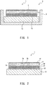
- an optical wavelength converter 1 of the present embodiment is accommodated in a box-like or plate-like ceramic package (container or substrate) 3 formed of, for example, alumina.
- a combination of the package 3 and the optical wavelength converter 1 accommodated therein will be referred to as a composite optical device 5.
- the term “accommodated” also refers to the case where the optical wavelength converter 1 is mounted on a substrate.
- the optical wavelength converter 1 includes a plate-like layered unit 11 including an optical wavelength conversion member 9, and a plate-like heat dissipation member 13, wherein the layered unit 11 is bonded to the dissipation member 13 by means of a layer-form bonding portion 15.
- an antireflective film 17, the optical wavelength conversion member 9, a reflective film 19, an intermediate film 21, the bonding portion 15, and the heat dissipation member 13 are disposed (specifically, stacked) such that they are arranged in this order from the light incident side (the upper side in FIG. 2 ) .
- light is applied to the optical wavelength converter 1 from the upper or lateral side in FIG. 2 .
- laser light is applied to the surface (upper surface: first surface 9a) of the antireflective film 17 from, for example, a laser light-emitting device (not illustrated).
- the antireflective film 17 has a light reflectance lower than that of the optical wavelength conversion member 9.
- the antireflective film 17 is a thin film which reduces the reflection of light from the outside, to thereby efficiently take the light from the outside into the optical wavelength conversion member 9.
- the antireflective film 17 is a thin film formed of, for example, one material selected from among niobium oxide, titanium oxide, tantalum oxide, aluminum oxide, zirconium oxide, silicon oxide, aluminum nitride, silicon nitride, and magnesium fluoride.
- the antireflective film 17 may have a single-layer structure formed of the aforementioned material, or a multilayer structure formed of the same material or different materials.
- the antireflective film 17 has a thickness of, for example, 0.01 ⁇ m to 1 ⁇ m. When the thickness of the antireflective film 17 is less than 0.01 ⁇ m, the antireflective effect is reduced. Meanwhile, when the thickness exceeds 1 ⁇ m, the antireflective film 17 absorbs a large amount of light, leading to light attenuation. Thus, the optical wavelength conversion member 9 exhibits reduced emission intensity.
- the reflective film 19 is a thin film which reflects light transmitted through the optical wavelength conversion member 9 or fluorescence generated in the optical wavelength conversion member 9.
- the reflective film 19 is a thin film formed of, for example, one material selected from among aluminum, niobium oxide, titanium oxide, lanthanum oxide, tantalum oxide, yttrium oxide, gadolinium oxide, tungsten oxide, hafnium oxide, aluminum oxide, and silicon nitride.
- the reflective film 19 may have a single-layer structure formed of the aforementioned material, or a multilayer structure formed of the same material or different materials.
- the reflective film 19 has a thickness of, for example, 0.1 ⁇ m to 1 ⁇ m.
- the thickness of the reflective film 19 is less than 0.1 ⁇ m, light transmits therethrough, and the reflective effect is reduced. Meanwhile, when the thickness exceeds 1 ⁇ m, the reflective film 19 absorbs a large amount of light. Thus, the optical wavelength conversion member 9 exhibits reduced emission intensity or generates heat.
- the intermediate film 21 is provided for improving the bondability of the bonding portion 15.
- the intermediate film 21 improves the wettability of the solder.
- the intermediate film 21 is a thin film (e.g., plating film) formed of, for example, one material selected from among gold, silver, and nickel.
- the intermediate film 21 may have a single-layer structure formed of the aforementioned material, or a multilayer structure formed of the same material or different materials.
- the intermediate film 21 has a thickness of, for example, 0.01 ⁇ m to 1 ⁇ m.
- the thickness of the intermediate film 21 is less than 0.01 ⁇ m, for example, wettability is lowered, and bonding may fail to be achieved. Meanwhile, when the thickness exceeds 1 ⁇ m, thermal conductivity is lowered, and the heat dissipation effect may be impaired.
- the bonding portion 15 is a layer provided for bonding a component (specifically, the reflective film 19) on the optical wavelength conversion member 9 side to the heat dissipation member 13 (via the intermediate film 21).
- the bonding portion 15 is a layer (solidified layer) formed of, for example, one material selected from among solder, a metal brazing material, a silver paste, and an inorganic binder.
- the bonding portion 15 may have a single-layer structure formed of the aforementioned material, or a multilayer structure formed of the same material or different materials.
- the bonding portion 15 has a thickness of, for example, 0.01 ⁇ m to 100 ⁇ m.
- the thickness of the bonding portion 15 is less than 0.01 ⁇ m, the bonding strength may be low, resulting in separation of the members. Meanwhile, when the thickness exceeds 100 ⁇ m, a thermal expansion difference may increase between both sides of the bonding portion in the thickness direction thereof, resulting in separation of the members.
- the heat dissipation member 13 is a plate member for enhancing the heat dissipation ability of the optical wavelength conversion member 9; i.e., a plate member having a thermal conductivity higher than that of the optical wavelength conversion member 9.
- the heat dissipation member 13 is a plate member formed of, for example, one material selected from among copper, aluminum, and aluminum nitride.
- the heat dissipation member 13 may have a single-layer structure formed of the aforementioned material, or a multilayer structure formed of the same material or different materials.
- the heat dissipation member 13 has a thickness of, for example, 0.1 mm to 4 mm.
- a thickness of the heat dissipation member 13 is less than 0.1 mm, a sufficient heat dissipation effect may fail to be achieved. Meanwhile, when the thickness exceeds 4 mm, a thermal expansion difference may increase between both sides of the heat dissipation member in the thickness direction thereof, resulting in separation of the member.
- the composite optical device 5 As shown in FIG. 1 , in the composite optical device 5, light emitted from a light-emitting element transmits through the antireflective film 17 and enters the translucent optical wavelength conversion member 9, and the wavelength of a portion of the light is converted in the interior of the optical wavelength conversion member 9. Thus, the optical wavelength conversion member 9 emits fluorescence having a wavelength different from that of the light emitted from the light-emitting element.
- a portion of the fluorescence generated in the optical wavelength conversion member 9 is emitted through the antireflective film 17 to the outside of the composite optical device 5 (e.g., upward in FIG. 1 ).
- the light transmitted through the optical wavelength conversion member 9 or the remaining portion of the fluorescence generated in the optical wavelength conversion member 9 is reflected by the reflective film 19 and then enters the optical wavelength conversion member 9. Thereafter, the light is emitted through the antireflective film 17 to the outside of the composite optical device 5 (e.g., upward in FIG. 1 ).
- the optical wavelength conversion member 9 converts the wavelength of blue light emitted from an LD, whereby the optical wavelength conversion member 9 as a whole emits white light to the outside of the composite optical device 5 (e.g., upward in FIG. 1 ).
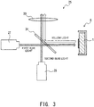
- the aforementioned composite optical device 5 is used in, for example, a light source unit 25 shown in FIG. 3 .
- the light source unit 25 includes the composite optical device 5, well-known blue light lasers (i.e., a first blue light laser 27 and a second blue light laser 29) (including, for example, light-emitting elements), a dichroic mirror 31, and a lens 33.
- well-known blue light lasers i.e., a first blue light laser 27 and a second blue light laser 29
- a dichroic mirror 31 including, for example, light-emitting elements
- the package 3 of the composite optical device 5 may have a light-emitting element mounting region on which a light-emitting element (e.g., LED or LD) is mounted.
- a light-emitting element e.g., LED or LD
- laser light i.e., first blue light
- the optical wavelength converter 1 of the composite optical device 5 (rightward in FIG. 3 ).
- the wavelength of the first blue light is converted by the optical wavelength converter 1, and the resultant yellow light is reflected and outputted leftward in FIG. 3 .
- the yellow light is reflected by the dichroic mirror 31 inclined by 45° with respect to the horizontal direction in FIG. 3 and then applied to the lens 33. Meanwhile, the second blue light applied from the second blue light laser 29 toward the lens 33 (upward in FIG. 3 ) transmits through the dichroic mirror 31 and then reaches the lens 33.
- the first blue light and the yellow light applied to the lens 33 are mixed together, and the resultant white light is outputted upward in FIG. 3 through the lens 33.
- optical wavelength conversion member 9 will now be described.
- the optical wavelength conversion member 9 of the present embodiment is formed of a ceramic sintered body having a fluorescent phase containing fluorescent crystal grains (i.e., fluorescent phase grains) as a main component and a translucent phase containing translucent crystal grains (i.e., fluorescent phase grains) as a main component.
- the crystal grains of the translucent phase have a composition of Al 2 O 3
- the crystal grains of the fluorescent phase have a composition represented by the formula A 3 B 5 O 12 :Ce.
- Each of the elements A and B is at least one element selected from the following element groups:
- the crystal grains of the translucent phase have a composition of Al 2 O 3
- the crystal grains of the fluorescent phase have a composition represented by the formula A 3 B 5 O 12 :Ce.
- Each of the elements A and B is at least one element selected from the following element groups.
- a and B of the formula A 3 B 5 O 12 :Ce are elements (different elements) of a substance represented by the formula A 3 B 5 O 12 :Ce (a substance having a so-called garnet structure) .
- O is oxygen
- Ce is cerium.
- the compound represented by the formula A 3 B 5 O 12 :Ce is, for example, a compound represented by the formula Y 3 Al 5 O 12 :Ce (a so-called YAG compound).
- the optical wavelength conversion member 9 has a thickness of 100 ⁇ m to 400 ⁇ m as measured from the first surface 9a (i.e., the upper surface of the optical wavelength conversion member 9) to the second surface 9b (i.e., the lower surface of the optical wavelength conversion member 9).
- the first surface 9a of the optical wavelength conversion member 9 has an average surface roughness (arithmetic average roughness Sa) satisfying the following relation: 0.001 ⁇ m ⁇ Sa ⁇ 0.5 ⁇ m.
- the first surface 1a of the optical wavelength conversion member 9 has a surface roughness (arithmetic average roughness Ra) satisfying the following relation: 0.001 ⁇ m ⁇ Ra ⁇ 0.4 ⁇ m.
- the amount of the compound represented by the formula A 3 B 5 O 12 :Ce is, for example, 3 vol.% to 70 vol.% relative to the entire ceramic sintered body.
- the Ce concentration is, for example, 0.1 mol% to 1.0 mol% relative to the element A of the compound.
- the refractive indices are as shown in Table 1 below.
- Table 1 Member Material Refractive index Anti reflective film SiO 2 1.38 MgF 2 1.46 Optical wavelength conversion member Al 2 O 3 -A 3 B 5 O 12 :Ce 1.76 ⁇ 1.85
- the optical wavelength conversion members 9 formed of the aforementioned materials and the antireflective films 17 formed of the aforementioned materials are selectively used in combination, the relative refractive index difference of each combination is as shown in Table 2 below.
- the resultant granules were then subjected to press forming.
- the resultant pressed compact was fired at a predetermined temperature for a predetermined period of time, to thereby produce a ceramic sintered body.
- the production method for the ceramic sintered body is not limited to the aforementioned production method in which the ceramic sintered body is produced by press forming.
- the ceramic sintered body may be produced through firing of a sheet compact prepared through sheet forming of the slurry.
- the antireflective film 17 was formed on the first surface 9a of the optical wavelength conversion member 9 (i.e., ceramic sintered body) by means of, for example, sputtering.
- the optical wavelength conversion member 9 i.e., ceramic sintered body
- the reflective film 19 was formed on the second surface 9b of the optical wavelength conversion member 9 by means of, for example, sputtering.
- the intermediate film 21 was formed on the surface of the reflective film 19 by means of, for example, sputtering.
- the intermediate film 21 may be formed by means of, for example, plating instead of sputtering.
- the intermediate film 21 may be formed by thermocompression bonding of a metal sheet (e.g., a Ni sheet).
- the layered unit 11 (specifically, the intermediate film 21) was bonded to the heat dissipation member 13 by use of a well-known bonding material such as solder (i.e., the layered unit 11 was soldered to the heat dissipation member 13).
- a well-known bonding material such as solder
- the optical wavelength converter 1 was bonded to the surface of a bottom portion of the container 3 by use of, for example, an adhesive, to thereby produce the composite optical device 5.
- optical wavelength converter samples (samples Nos. 1 to 32) shown in Tables 3 and 4 below; i.e., optical wavelength converter samples of Examples 1 to 5.
- Laser light having a wavelength of 465 nm (i.e., blue LD light) was focused to a width of 0.1 mm by means of a lens, and each sample was irradiated with the focused light.
- the chromaticity (in X-direction) of light reflected by the sample was measured by means of a spectroradiometer (CL-500A, manufactured by KONICA MINOLTA, INC.). During the chromaticity measurement, the power density of blue LD light was gradually increased from 0 to 100 W/mm 2 .
- Occurrence of temperature quenching was determined when the chromaticity was reduced to 60% or less of that at a laser power density of 5 W/mm 2 .
- the laser power density at occurrence of temperature quenching is shown in Table 4 below. For a sample exhibiting no quenching even at 100 W/mm 2 , the laser power density at occurrence of temperature quenching is represented by ">100.” A sample exhibiting no temperature quenching at 100 W/mm 2 or more is preferred in terms of laser output resistance.
- Blue LD light having a wavelength of 465 nm was focused to a width of 0.1 mm by means of a lens, and each sample was irradiated with the focused light.
- Light reflected by the sample was focused by means of a lens, and the emission intensity (i.e., fluorescence intensity) was measured by means of a power sensor.
- the sample was irradiated with the light at a power density of 40 W/mm 2 .
- the fluorescence intensity was evaluated by a value (%) relative to that (taken as 100) of a YAG:Ce single-crystal body.
- the fluorescence intensity is preferably 100% or more.
- Color unevenness (variation in color) was evaluated through determination of a variation in chromaticity by means of an illuminometer.
- blue LD light having a wavelength of 465 nm was focused to a width of 0.5 mm by means of a lens, and each sample was irradiated with the focused light.
- the chromaticity of light reflected by the sample was measured by means of a spectroradiometer (CL-500A, manufactured by KONICA MINOLTA, INC.).
- the light irradiation was performed on a 9 mm square region (divided into nine regions at intervals of 3 mm) at the center of the surface of each sample (i.e., the first surface of the sample).
- a variation in chromaticity (in X-direction) i.e., ⁇ x was evaluated in each of the nine regions.
- the results are shown in Table 4 below.
- the term "variation in chromaticity ( ⁇ x)" refers to the maximum deviation of chromaticity (in X-direction).
- the variation in chromaticity ⁇ x is preferably less than 0.03.
- chromaticity refers to a chromaticity indicated by the CIE-XYZ color system (international color system) established by the International Commission on Illumination (CIE) in 1931. Specifically, the chromaticity is indicated by the xy chromaticity diagram (so-called CIE chromaticity diagram) wherein three primary colors of light are digitized and represented in an xy coordinate space.
- the average roughness (arithmetic average roughness Ra) and average surface roughness (arithmetic average roughness Sa) of the first surface of the optical wavelength converter were measured by means of a non-contact three-dimensional measuring apparatus Infinite Focus G5 (manufactured by Alicona Imaging).
- the arithmetic average roughness Ra is a parameter prescribed by JIS B 0601:2013.
- the arithmetic average roughness Ra was measured at any five points of the sample. The averaged value is shown in Table 4 below.
- the arithmetic average roughness Sa is a three-dimensional extension of two-dimensional arithmetic average roughness Ra and is a parameter prescribed by ISO 25178. The results of measurement are shown in Table 4 below.
- the average roughness (arithmetic average roughness Ra) of the first surface of the optical wavelength converter was measured by the method described below.
- each sample was cut in a thickness direction so as to observe the layered structure of the sample, and images ( ⁇ 10,000) were obtained at any five points of the cut surface (see, for example, FIG. 4(b) ).
- the images were subjected to image processing, and the arithmetic average roughness Ra of the surface of the fluorescent body (i.e., optical wavelength conversion member) was measured according to JIS B 0601:2013, to thereby calculate a five-point average.
- the results are shown in the "two-dimensional surface roughness Ra" column of Table 4 below.
- Table 3 shows the type of the fluorescent body (optical wavelength conversion member), the types of elements A and B, the presence or absence of the antireflective film, the presence or absence of the reflective film, the presence or absence of the intermediate film, and the thickness of the fluorescent body for each sample.
- the thickness of the fluorescent body (16 mm ⁇ 16 mm) was measured at its center and end portions (at four points in total) by means of a micrometer, and the thus-measured thicknesses were averaged.
- Optical wavelength converter samples (Nos. 1 to 12) were prepared under the conditions shown in, for example, Table 3 below.
- Al 2 O 3 powder (mean particle size: 0.2 ⁇ m), Y 2 O 3 powder (mean particle size: 1.2 ⁇ m), Lu 2 O 3 powder (mean particle size: 1.1 ⁇ m), Sc 2 O 3 powder (mean particle size: 1.2 ⁇ m), CeO 2 powder (mean particle size: 1.5 ⁇ m), Gd 2 O 3 powder (mean particle size: 1.1 ⁇ m), and Ga 2 O 3 powder (mean particle size: 1.1 ⁇ m) were weighed in accordance with the composition of the ceramic sintered body of the optical wavelength converter of each sample (i.e., Al 2 O 3 -A 3 B 5 O 12 :Ce).
- the powder materials were weighed so that the A 3 B 5 O 12 :Ce content of the entire ceramic sintered body was adjusted to 30 vol.%.
- the Gd or Ga content was adjusted to 15 mol% relative to the element A or B, respectively.
- the resultant fluorescent body was processed into dimensions of 16 mm ⁇ 16 mm ⁇ 200 ⁇ m (thickness).
- an SiO 2 antireflective film (thickness: 1 ⁇ m) was formed on the upper surface (first surface) of the thus-processed fluorescent body by means of sputtering.
- An Al reflective film (thickness: 1 ⁇ m) was formed on the lower surface (second surface) of the fluorescent body by means of sputtering.
- Ni intermediate film thickness: 1 ⁇ m
- the fluorescent body provided with the antireflective film, the reflective film, and the intermediate film was cut into a piece of 3.5 mm ⁇ 3.5 mm.
- a heat dissipation substrate i.e., heat dissipation member formed of a copper plate was processed into dimensions of 12 mm ⁇ 12 mm ⁇ 1.5 mm (thickness).
- the fluorescent body was then bonded to the heat dissipation substrate.
- the fluorescent body (specifically, the intermediate film) was soldered to the heat dissipation substrate by means of a bonding material (i.e., solder, such as solder containing Pb as a main component, or Pb-free solder) placed between the fluorescent body and the heat dissipation substrate.
- solder such as solder containing Pb as a main component, or Pb-free solder
- the samples falling within the scope of the present disclosure exhibited good results; i.e., high laser output resistance (i.e., no temperature quenching at 100 W/mm 2 ), a high fluorescence intensity of 110% or more, and a small variation in color (color unevenness) of 0.028 or less.
- the ceramic sintered body exhibited a relative density of 99% or more in all the samples. The same results were obtained in the samples of Examples 2 to 5.
- Optical wavelength converter samples (Nos. 13 and 14) falling outside the scope of the present disclosure were prepared under the conditions shown in, for example, Table 3 below and evaluated in the same manner as in Example 1.
- Example 2 The preparation method for the samples of Example 2 is basically the same as in Example 1.
- the type of the fluorescent body is different from that in Example 1. Specifically, the fluorescent body in sample No. 13 is formed by dispersing YAG particles in a resin, and the fluorescent body in sample No. 14 is formed of a YAG single-crystal.
- Example 2 exhibited insufficient laser output resistance (i.e., 75 W/mm 2 or less). This is probably due to the fact that a low thermal conductivity of the fluorescent body causes generation of a large amount of heat, resulting in occurrence of temperature quenching.
- Optical wavelength converter samples (Nos. 15 to 17) falling outside the scope of the present disclosure were prepared under the conditions shown in, for example, Table 3 below and evaluated in the same manner as in Example 1.
- Example 3 The preparation method for the samples of Example 3 is basically the same as in Example 1.
- sample No. 15 does not include an antireflective film
- sample No. 16 does not include a reflective film
- sample No. 17 does not include an intermediate film.
- Optical wavelength converter samples (Nos. 18 to 26) falling within the scope of the present disclosure were prepared under the conditions shown in, for example, Table 3 below and evaluated in the same manner as in Example 1.
- Example 4 The preparation method for the samples of Example 4 is basically the same as in Example 1. However, the thickness of the fluorescent body was varied within a range of 50 ⁇ m to 450 ⁇ m in the samples.
- samples Nos. 19 to 25 in which the thickness of the fluorescent body was 100 ⁇ m to 400 ⁇ m, were good, because samples Nos. 19 to 25 exhibited higher fluorescence intensity as compared with samples Nos. 18 and 26 and maintained fluorescence at high laser output.
- sample No. 18 in which the thickness of the fluorescent body was less than 100 ⁇ m, exhibited low fluorescence intensity due to a decrease in the amount of a fluorescent component in a transmission direction (i.e., insufficient fluorescence).
- Sample No. 26 in which the thickness of the fluorescent body was more than 400 ⁇ m, exhibited low fluorescence intensity due to an increase in the amount of light absorbed in the interior of the fluorescent body, which increase was caused by the large thickness of the fluorescent body.
- Optical wavelength converter samples (Nos. 27 to 32) falling within the scope of the present disclosure were prepared under the conditions shown in, for example, Table 3 below and evaluated in the same manner as in Example 1.
- Example 5 The preparation method for the samples of Example 5 is basically the same as in Example 1.
- the arithmetic average roughness Sa of the first surface of the fluorescent body was varied within a range of 0.0008 ⁇ m to 0.5 ⁇ m in the samples.
- the arithmetic average roughness Sa can be changed by a surface treatment (e.g., mechanical polishing or blasting) of the surface of the fluorescent body.
- samples Nos. 28 to 31 in which the arithmetic average roughness Sa satisfied the relation: 0.001 ⁇ m ⁇ Sa ⁇ 0.5 ⁇ m, and the arithmetic average roughness Ra satisfied the relation: 0.001 ⁇ m ⁇ Ra ⁇ 0.4 ⁇ m, were good because samples Nos. 28 to 31 exhibited higher fluorescence intensity as compared with samples Nos. 27 and 32.
- sample No. 27 in which the arithmetic average roughness Sa of the surface of the fluorescent body was less than 0.0001 ⁇ m, exhibited low fluorescence intensity due to an increase in the amount of light reflected at the surface of the fluorescent body.
- sample No. 32 in which the arithmetic average roughness Sa of the surface of the fluorescent body was more than 0.5 ⁇ m, exhibited low fluorescence intensity due to inefficient extraction of emitted light caused by diffused reflection at the surface of the fluorescent body.
Landscapes
- Chemical & Material Sciences (AREA)
- Engineering & Computer Science (AREA)
- Physics & Mathematics (AREA)
- Ceramic Engineering (AREA)
- General Engineering & Computer Science (AREA)
- Organic Chemistry (AREA)
- Materials Engineering (AREA)
- Manufacturing & Machinery (AREA)
- Optics & Photonics (AREA)
- General Physics & Mathematics (AREA)
- Structural Engineering (AREA)
- Composite Materials (AREA)
- Electromagnetism (AREA)
- Condensed Matter Physics & Semiconductors (AREA)
- Inorganic Chemistry (AREA)
- Spectroscopy & Molecular Physics (AREA)
- Optical Filters (AREA)
- Semiconductor Lasers (AREA)
- Non-Portable Lighting Devices Or Systems Thereof (AREA)
- Luminescent Compositions (AREA)
Applications Claiming Priority (2)
| Application Number | Priority Date | Filing Date | Title |
|---|---|---|---|
| JP2017191058A JP7120745B2 (ja) | 2017-09-29 | 2017-09-29 | 光波長変換装置及び光複合装置 |
| PCT/JP2018/033392 WO2019065175A1 (fr) | 2017-09-29 | 2018-09-10 | Convertisseur de longueur d'onde optique et dispositif optique composite |
Publications (3)
| Publication Number | Publication Date |
|---|---|
| EP3690497A1 true EP3690497A1 (fr) | 2020-08-05 |
| EP3690497A4 EP3690497A4 (fr) | 2021-06-09 |
| EP3690497B1 EP3690497B1 (fr) | 2024-11-20 |
Family
ID=65901846
Family Applications (1)
| Application Number | Title | Priority Date | Filing Date |
|---|---|---|---|
| EP18862586.7A Active EP3690497B1 (fr) | 2017-09-29 | 2018-09-10 | Convertisseur de longueur d'onde optique et dispositif optique composite |
Country Status (7)
| Country | Link |
|---|---|
| US (1) | US11316078B2 (fr) |
| EP (1) | EP3690497B1 (fr) |
| JP (1) | JP7120745B2 (fr) |
| KR (1) | KR102470285B1 (fr) |
| CN (1) | CN111133343B (fr) |
| TW (1) | TWI696685B (fr) |
| WO (1) | WO2019065175A1 (fr) |
Families Citing this family (17)
| Publication number | Priority date | Publication date | Assignee | Title |
|---|---|---|---|---|
| JP7111989B2 (ja) * | 2019-04-22 | 2022-08-03 | 日亜化学工業株式会社 | 波長変換部品、波長変換部品の製造方法、及び、発光装置 |
| DE102020117119A1 (de) * | 2019-07-04 | 2021-03-18 | Schott Ag | Optisches Konverterrad |
| CN112443818B (zh) * | 2019-08-30 | 2023-04-28 | 深圳市中光工业技术研究院 | 光源系统及照明装置 |
| DE102021116016A1 (de) * | 2020-06-29 | 2021-12-30 | Panasonic Intellectual Property Management Co., Ltd. | Wellenlängenumwandlungsvorrichtung, projektor und fluoreszierendes keramikelement |
| JP7706071B2 (ja) * | 2020-06-29 | 2025-07-11 | パナソニックIpマネジメント株式会社 | 波長変換デバイス及びプロジェクタ |
| JP7617364B2 (ja) | 2020-08-07 | 2025-01-20 | 日亜化学工業株式会社 | 希土類アルミン酸塩焼結体及びその製造方法 |
| JP7633520B2 (ja) * | 2021-07-07 | 2025-02-20 | 日亜化学工業株式会社 | 発光装置 |
| JP2023031714A (ja) * | 2021-08-25 | 2023-03-09 | Tdk株式会社 | 透明蛍光体および光源装置 |
| JP2023056465A (ja) * | 2021-10-07 | 2023-04-19 | パナソニックIpマネジメント株式会社 | 蛍光体デバイス及び発光装置 |
| WO2023058541A1 (fr) * | 2021-10-07 | 2023-04-13 | パナソニックIpマネジメント株式会社 | Dispositif à luminophore et dispositif électroluminescent |
| JP7832451B2 (ja) * | 2021-12-22 | 2026-03-18 | 日亜化学工業株式会社 | 波長変換部材及び発光装置 |
| JP7767257B2 (ja) * | 2021-12-28 | 2025-11-11 | クアーズテック合同会社 | セラミックス蛍光体プレート |
| JPWO2023153241A1 (fr) | 2022-02-09 | 2023-08-17 | ||
| JP7704050B2 (ja) * | 2022-03-03 | 2025-07-08 | 信越化学工業株式会社 | ガーネット型透明セラミックスのレーザー損傷閾値の改善方法 |
| CN116040965B (zh) * | 2023-01-31 | 2024-02-27 | 宁波启朴芯微系统技术有限公司 | 一种宽频减反膜及其制备方法和应用 |
| JP2024122576A (ja) * | 2023-02-28 | 2024-09-09 | 日亜化学工業株式会社 | 焼結体の製造方法及び焼結体 |
| CN117623746B (zh) * | 2023-10-27 | 2025-08-05 | 深圳市光粒子技术有限公司 | 波长转换装置及其制备方法 |
Family Cites Families (27)
| Publication number | Priority date | Publication date | Assignee | Title |
|---|---|---|---|---|
| JP3116727B2 (ja) * | 1994-06-17 | 2000-12-11 | 日亜化学工業株式会社 | 面状光源 |
| CA2308933C (fr) * | 1999-05-19 | 2008-07-22 | Ngk Spark Plug Co., Ltd. | Ceramique polycristalline translucide et methode de fabrication |
| JP3749243B2 (ja) * | 2001-09-03 | 2006-02-22 | 松下電器産業株式会社 | 半導体発光デバイス,発光装置及び半導体発光デバイスの製造方法 |
| WO2003080764A1 (fr) * | 2002-03-22 | 2003-10-02 | Nichia Corporation | Phosphore de nitrure, procede de preparation de phosphore de nitrure et diode electroluminescente |
| JP2005166313A (ja) * | 2003-11-28 | 2005-06-23 | Ngk Spark Plug Co Ltd | 色素増感型太陽電池 |
| JP5083211B2 (ja) | 2006-06-22 | 2012-11-28 | 宇部興産株式会社 | 光変換用複合体、それを用いた発光装置および色調制御方法 |
| TW201132740A (en) * | 2009-09-25 | 2011-10-01 | Panasonic Elec Works Co Ltd | Wavelength converting particle, wavelength converting member including same, and light-emitting device |
| JP2012243624A (ja) | 2011-05-20 | 2012-12-10 | Stanley Electric Co Ltd | 光源装置および照明装置 |
| JP2013055269A (ja) * | 2011-09-06 | 2013-03-21 | Nippon Electric Glass Co Ltd | 波長変換部材および発光デバイス |
| CN103367611B (zh) | 2012-03-28 | 2017-08-08 | 日亚化学工业株式会社 | 波长变换用无机成型体及其制造方法以及发光装置 |
| JP5966501B2 (ja) * | 2012-03-28 | 2016-08-10 | 日亜化学工業株式会社 | 波長変換用無機成形体及びその製造方法、並びに発光装置 |
| CN103374348B (zh) * | 2012-04-27 | 2017-05-24 | 晶元光电股份有限公司 | 波长转换物质 |
| JP5888124B2 (ja) | 2012-05-30 | 2016-03-16 | 株式会社ニデック | 多層膜フィルタ、及び多層膜フィルタの製造方法 |
| CN107193180B (zh) | 2012-08-02 | 2020-07-28 | 日亚化学工业株式会社 | 波长转换装置 |
| TWI597349B (zh) * | 2012-09-21 | 2017-09-01 | 住友大阪水泥股份有限公司 | 複合波長變換粉體、含有複合波長變換粉體的樹脂組成物及發光裝置 |
| WO2014061497A1 (fr) * | 2012-10-16 | 2014-04-24 | コニカミノルタ株式会社 | Miroir à film et appareil réfléchissant pour génération d'énergie thermique solaire |
| WO2014123145A1 (fr) * | 2013-02-08 | 2014-08-14 | ウシオ電機株式会社 | Dispositif de source de lumière fluorescente |
| JP6075712B2 (ja) | 2013-03-25 | 2017-02-08 | ウシオ電機株式会社 | 発光デバイス |
| JP6253392B2 (ja) | 2013-12-18 | 2017-12-27 | スタンレー電気株式会社 | 発光装置及びそれを用いたプロジェクター用光源 |
| MY177277A (en) * | 2014-03-03 | 2020-09-10 | Covalent Mat Corporation | Wavelength converting member |
| JP2016027613A (ja) * | 2014-05-21 | 2016-02-18 | 日本電気硝子株式会社 | 波長変換部材及びそれを用いた発光装置 |
| US9534741B2 (en) * | 2014-07-23 | 2017-01-03 | Cree, Inc. | Lighting devices with illumination regions having different gamut properties |
| JP2017090625A (ja) * | 2015-11-09 | 2017-05-25 | 日本碍子株式会社 | 光学部品及びその製造方法 |
| JP6741982B2 (ja) | 2015-12-24 | 2020-08-19 | パナソニックIpマネジメント株式会社 | 発光素子および照明装置 |
| KR102556400B1 (ko) * | 2016-01-12 | 2023-07-18 | 쑤저우 레킨 세미컨덕터 컴퍼니 리미티드 | 발광소자 패키지 |
| JP6620621B2 (ja) | 2016-03-18 | 2019-12-18 | セイコーエプソン株式会社 | 波長変換素子、照明装置およびプロジェクター |
| CN108954039B (zh) * | 2017-05-19 | 2020-07-03 | 深圳光峰科技股份有限公司 | 波长转换装置及其制备方法 |
-
2017
- 2017-09-29 JP JP2017191058A patent/JP7120745B2/ja active Active
-
2018
- 2018-09-10 EP EP18862586.7A patent/EP3690497B1/fr active Active
- 2018-09-10 US US16/651,434 patent/US11316078B2/en active Active
- 2018-09-10 CN CN201880061679.1A patent/CN111133343B/zh active Active
- 2018-09-10 KR KR1020207008506A patent/KR102470285B1/ko active Active
- 2018-09-10 WO PCT/JP2018/033392 patent/WO2019065175A1/fr not_active Ceased
- 2018-09-27 TW TW107134142A patent/TWI696685B/zh active
Also Published As
| Publication number | Publication date |
|---|---|
| US20200303597A1 (en) | 2020-09-24 |
| KR102470285B1 (ko) | 2022-11-23 |
| EP3690497A4 (fr) | 2021-06-09 |
| TW201920608A (zh) | 2019-06-01 |
| JP7120745B2 (ja) | 2022-08-17 |
| TWI696685B (zh) | 2020-06-21 |
| KR20200042933A (ko) | 2020-04-24 |
| EP3690497B1 (fr) | 2024-11-20 |
| US11316078B2 (en) | 2022-04-26 |
| CN111133343B (zh) | 2022-04-29 |
| CN111133343A (zh) | 2020-05-08 |
| JP2019066632A (ja) | 2019-04-25 |
| WO2019065175A1 (fr) | 2019-04-04 |
Similar Documents
| Publication | Publication Date | Title |
|---|---|---|
| EP3690497B1 (fr) | Convertisseur de longueur d'onde optique et dispositif optique composite | |
| JP6253392B2 (ja) | 発光装置及びそれを用いたプロジェクター用光源 | |
| EP3588151A1 (fr) | Élément de conversion de longueur d'onde de lumière et dispositif d'émission lumineuse | |
| EP3816682B1 (fr) | Pièce de conversion de longueur d'onde optique, dispositif de conversion de longueur d'onde optique et dispositif électroluminescent | |
| EP3754386A1 (fr) | Dispositif de conversion de longueur d'onde optique | |
| JP2012089316A (ja) | 光源装置および照明装置 | |
| EP4488345A1 (fr) | Céramique composite, élément de phosphore, dispositif d'éclairage laser et procédé de production de céramique composite | |
| JP7188893B2 (ja) | 光波長変換部材及び光波長変換装置 | |
| US20240060623A1 (en) | Lighting device | |
| US20240059965A1 (en) | Lighting device | |
| CN108692204B (zh) | 荧光光源装置 | |
| JP7387898B2 (ja) | 蛍光板、波長変換部材、および、光源装置 | |
| JP7244297B2 (ja) | 光波長変換部品 | |
| WO2019021846A1 (fr) | Élément de conversion de longueur d'onde et dispositif électroluminescent | |
| WO2024047888A1 (fr) | Dispositif à luminophore | |
| TWI802898B (zh) | 螢光板、波長轉換構件及光源裝置 | |
| US11754259B2 (en) | Fluorescent plate, wavelength conversion member, and light source device | |
| WO2025053256A1 (fr) | Céramique composite, élément fluorescent, dispositif d'éclairage laser et procédé de production de céramique composite | |
| JP2025087512A (ja) | 波長変換部材、および発光装置 |
Legal Events
| Date | Code | Title | Description |
|---|---|---|---|
| STAA | Information on the status of an ep patent application or granted ep patent |
Free format text: STATUS: THE INTERNATIONAL PUBLICATION HAS BEEN MADE |
|
| PUAI | Public reference made under article 153(3) epc to a published international application that has entered the european phase |
Free format text: ORIGINAL CODE: 0009012 |
|
| STAA | Information on the status of an ep patent application or granted ep patent |
Free format text: STATUS: REQUEST FOR EXAMINATION WAS MADE |
|
| 17P | Request for examination filed |
Effective date: 20200320 |
|
| AK | Designated contracting states |
Kind code of ref document: A1 Designated state(s): AL AT BE BG CH CY CZ DE DK EE ES FI FR GB GR HR HU IE IS IT LI LT LU LV MC MK MT NL NO PL PT RO RS SE SI SK SM TR |
|
| AX | Request for extension of the european patent |
Extension state: BA ME |
|
| DAV | Request for validation of the european patent (deleted) | ||
| DAX | Request for extension of the european patent (deleted) | ||
| A4 | Supplementary search report drawn up and despatched |
Effective date: 20210507 |
|
| RIC1 | Information provided on ipc code assigned before grant |
Ipc: G02B 5/20 20060101AFI20210430BHEP Ipc: C04B 35/117 20060101ALI20210430BHEP Ipc: C09K 11/80 20060101ALI20210430BHEP Ipc: F21S 2/00 20160101ALI20210430BHEP Ipc: F21V 7/30 20180101ALI20210430BHEP Ipc: F21V 9/32 20180101ALI20210430BHEP Ipc: F21V 29/502 20150101ALI20210430BHEP Ipc: H01L 33/50 20100101ALI20210430BHEP Ipc: H01S 5/022 20210101ALI20210430BHEP Ipc: F21Y 115/10 20160101ALI20210430BHEP Ipc: F21Y 115/30 20160101ALI20210430BHEP Ipc: C09K 11/08 20060101ALI20210430BHEP |
|
| STAA | Information on the status of an ep patent application or granted ep patent |
Free format text: STATUS: EXAMINATION IS IN PROGRESS |
|
| 17Q | First examination report despatched |
Effective date: 20230321 |
|
| RAP3 | Party data changed (applicant data changed or rights of an application transferred) |
Owner name: NGK SPARK PLUG CO., LTD. |
|
| RAP3 | Party data changed (applicant data changed or rights of an application transferred) |
Owner name: NITERRA CO., LTD. |
|
| GRAP | Despatch of communication of intention to grant a patent |
Free format text: ORIGINAL CODE: EPIDOSNIGR1 |
|
| STAA | Information on the status of an ep patent application or granted ep patent |
Free format text: STATUS: GRANT OF PATENT IS INTENDED |
|
| INTG | Intention to grant announced |
Effective date: 20240822 |
|
| GRAS | Grant fee paid |
Free format text: ORIGINAL CODE: EPIDOSNIGR3 |
|
| GRAA | (expected) grant |
Free format text: ORIGINAL CODE: 0009210 |
|
| STAA | Information on the status of an ep patent application or granted ep patent |
Free format text: STATUS: THE PATENT HAS BEEN GRANTED |
|
| AK | Designated contracting states |
Kind code of ref document: B1 Designated state(s): AL AT BE BG CH CY CZ DE DK EE ES FI FR GB GR HR HU IE IS IT LI LT LU LV MC MK MT NL NO PL PT RO RS SE SI SK SM TR |
|
| REG | Reference to a national code |
Ref country code: GB Ref legal event code: FG4D |
|
| REG | Reference to a national code |
Ref country code: CH Ref legal event code: EP |
|
| REG | Reference to a national code |
Ref country code: DE Ref legal event code: R096 Ref document number: 602018076824 Country of ref document: DE |
|
| REG | Reference to a national code |
Ref country code: IE Ref legal event code: FG4D |
|
| REG | Reference to a national code |
Ref country code: LT Ref legal event code: MG9D |
|
| REG | Reference to a national code |
Ref country code: NL Ref legal event code: MP Effective date: 20241120 |
|
| PG25 | Lapsed in a contracting state [announced via postgrant information from national office to epo] |
Ref country code: HR Free format text: LAPSE BECAUSE OF FAILURE TO SUBMIT A TRANSLATION OF THE DESCRIPTION OR TO PAY THE FEE WITHIN THE PRESCRIBED TIME-LIMIT Effective date: 20241120 Ref country code: IS Free format text: LAPSE BECAUSE OF FAILURE TO SUBMIT A TRANSLATION OF THE DESCRIPTION OR TO PAY THE FEE WITHIN THE PRESCRIBED TIME-LIMIT Effective date: 20250320 Ref country code: PT Free format text: LAPSE BECAUSE OF FAILURE TO SUBMIT A TRANSLATION OF THE DESCRIPTION OR TO PAY THE FEE WITHIN THE PRESCRIBED TIME-LIMIT Effective date: 20250320 |
|
| PG25 | Lapsed in a contracting state [announced via postgrant information from national office to epo] |
Ref country code: FI Free format text: LAPSE BECAUSE OF FAILURE TO SUBMIT A TRANSLATION OF THE DESCRIPTION OR TO PAY THE FEE WITHIN THE PRESCRIBED TIME-LIMIT Effective date: 20241120 Ref country code: NL Free format text: LAPSE BECAUSE OF FAILURE TO SUBMIT A TRANSLATION OF THE DESCRIPTION OR TO PAY THE FEE WITHIN THE PRESCRIBED TIME-LIMIT Effective date: 20241120 |
|
| REG | Reference to a national code |
Ref country code: AT Ref legal event code: MK05 Ref document number: 1744078 Country of ref document: AT Kind code of ref document: T Effective date: 20241120 |
|
| PG25 | Lapsed in a contracting state [announced via postgrant information from national office to epo] |
Ref country code: BG Free format text: LAPSE BECAUSE OF FAILURE TO SUBMIT A TRANSLATION OF THE DESCRIPTION OR TO PAY THE FEE WITHIN THE PRESCRIBED TIME-LIMIT Effective date: 20241120 |
|
| PG25 | Lapsed in a contracting state [announced via postgrant information from national office to epo] |
Ref country code: ES Free format text: LAPSE BECAUSE OF FAILURE TO SUBMIT A TRANSLATION OF THE DESCRIPTION OR TO PAY THE FEE WITHIN THE PRESCRIBED TIME-LIMIT Effective date: 20241120 |
|
| PG25 | Lapsed in a contracting state [announced via postgrant information from national office to epo] |
Ref country code: NO Free format text: LAPSE BECAUSE OF FAILURE TO SUBMIT A TRANSLATION OF THE DESCRIPTION OR TO PAY THE FEE WITHIN THE PRESCRIBED TIME-LIMIT Effective date: 20250220 |
|
| PG25 | Lapsed in a contracting state [announced via postgrant information from national office to epo] |
Ref country code: LV Free format text: LAPSE BECAUSE OF FAILURE TO SUBMIT A TRANSLATION OF THE DESCRIPTION OR TO PAY THE FEE WITHIN THE PRESCRIBED TIME-LIMIT Effective date: 20241120 Ref country code: GR Free format text: LAPSE BECAUSE OF FAILURE TO SUBMIT A TRANSLATION OF THE DESCRIPTION OR TO PAY THE FEE WITHIN THE PRESCRIBED TIME-LIMIT Effective date: 20250221 Ref country code: AT Free format text: LAPSE BECAUSE OF FAILURE TO SUBMIT A TRANSLATION OF THE DESCRIPTION OR TO PAY THE FEE WITHIN THE PRESCRIBED TIME-LIMIT Effective date: 20241120 |
|
| PG25 | Lapsed in a contracting state [announced via postgrant information from national office to epo] |
Ref country code: PL Free format text: LAPSE BECAUSE OF FAILURE TO SUBMIT A TRANSLATION OF THE DESCRIPTION OR TO PAY THE FEE WITHIN THE PRESCRIBED TIME-LIMIT Effective date: 20241120 |
|
| PG25 | Lapsed in a contracting state [announced via postgrant information from national office to epo] |
Ref country code: RS Free format text: LAPSE BECAUSE OF FAILURE TO SUBMIT A TRANSLATION OF THE DESCRIPTION OR TO PAY THE FEE WITHIN THE PRESCRIBED TIME-LIMIT Effective date: 20250220 |
|
| PG25 | Lapsed in a contracting state [announced via postgrant information from national office to epo] |
Ref country code: SM Free format text: LAPSE BECAUSE OF FAILURE TO SUBMIT A TRANSLATION OF THE DESCRIPTION OR TO PAY THE FEE WITHIN THE PRESCRIBED TIME-LIMIT Effective date: 20241120 |
|
| PG25 | Lapsed in a contracting state [announced via postgrant information from national office to epo] |
Ref country code: DK Free format text: LAPSE BECAUSE OF FAILURE TO SUBMIT A TRANSLATION OF THE DESCRIPTION OR TO PAY THE FEE WITHIN THE PRESCRIBED TIME-LIMIT Effective date: 20241120 |
|
| PG25 | Lapsed in a contracting state [announced via postgrant information from national office to epo] |
Ref country code: EE Free format text: LAPSE BECAUSE OF FAILURE TO SUBMIT A TRANSLATION OF THE DESCRIPTION OR TO PAY THE FEE WITHIN THE PRESCRIBED TIME-LIMIT Effective date: 20241120 |
|
| PG25 | Lapsed in a contracting state [announced via postgrant information from national office to epo] |
Ref country code: RO Free format text: LAPSE BECAUSE OF FAILURE TO SUBMIT A TRANSLATION OF THE DESCRIPTION OR TO PAY THE FEE WITHIN THE PRESCRIBED TIME-LIMIT Effective date: 20241120 |
|
| PG25 | Lapsed in a contracting state [announced via postgrant information from national office to epo] |
Ref country code: SK Free format text: LAPSE BECAUSE OF FAILURE TO SUBMIT A TRANSLATION OF THE DESCRIPTION OR TO PAY THE FEE WITHIN THE PRESCRIBED TIME-LIMIT Effective date: 20241120 |
|
| PG25 | Lapsed in a contracting state [announced via postgrant information from national office to epo] |
Ref country code: CZ Free format text: LAPSE BECAUSE OF FAILURE TO SUBMIT A TRANSLATION OF THE DESCRIPTION OR TO PAY THE FEE WITHIN THE PRESCRIBED TIME-LIMIT Effective date: 20241120 |
|
| PG25 | Lapsed in a contracting state [announced via postgrant information from national office to epo] |
Ref country code: IT Free format text: LAPSE BECAUSE OF FAILURE TO SUBMIT A TRANSLATION OF THE DESCRIPTION OR TO PAY THE FEE WITHIN THE PRESCRIBED TIME-LIMIT Effective date: 20241120 |
|
| REG | Reference to a national code |
Ref country code: DE Ref legal event code: R097 Ref document number: 602018076824 Country of ref document: DE |
|
| PG25 | Lapsed in a contracting state [announced via postgrant information from national office to epo] |
Ref country code: SE Free format text: LAPSE BECAUSE OF FAILURE TO SUBMIT A TRANSLATION OF THE DESCRIPTION OR TO PAY THE FEE WITHIN THE PRESCRIBED TIME-LIMIT Effective date: 20241120 |
|
| PLBE | No opposition filed within time limit |
Free format text: ORIGINAL CODE: 0009261 |
|
| STAA | Information on the status of an ep patent application or granted ep patent |
Free format text: STATUS: NO OPPOSITION FILED WITHIN TIME LIMIT |
|
| PGFP | Annual fee paid to national office [announced via postgrant information from national office to epo] |
Ref country code: DE Payment date: 20250730 Year of fee payment: 8 |
|
| 26N | No opposition filed |
Effective date: 20250821 |