EP3693992B1 - Oberflächenmontiertes halbleiterbauelement und verfahren zur herstellung - Google Patents
Oberflächenmontiertes halbleiterbauelement und verfahren zur herstellung Download PDFInfo
- Publication number
- EP3693992B1 EP3693992B1 EP19156433.5A EP19156433A EP3693992B1 EP 3693992 B1 EP3693992 B1 EP 3693992B1 EP 19156433 A EP19156433 A EP 19156433A EP 3693992 B1 EP3693992 B1 EP 3693992B1
- Authority
- EP
- European Patent Office
- Prior art keywords
- lead frame
- major surface
- semiconductor device
- major
- semiconductor die
- Prior art date
- Legal status (The legal status is an assumption and is not a legal conclusion. Google has not performed a legal analysis and makes no representation as to the accuracy of the status listed.)
- Active
Links
Images


Classifications
-
- H—ELECTRICITY
- H10—SEMICONDUCTOR DEVICES; ELECTRIC SOLID-STATE DEVICES NOT OTHERWISE PROVIDED FOR
- H10W—GENERIC PACKAGES, INTERCONNECTIONS, CONNECTORS OR OTHER CONSTRUCTIONAL DETAILS OF DEVICES COVERED BY CLASS H10
- H10W70/00—Package substrates; Interposers; Redistribution layers [RDL]
- H10W70/60—Insulating or insulated package substrates; Interposers; Redistribution layers
- H10W70/62—Insulating or insulated package substrates; Interposers; Redistribution layers characterised by their interconnections
- H10W70/65—Shapes or dispositions of interconnections
-
- H—ELECTRICITY
- H10—SEMICONDUCTOR DEVICES; ELECTRIC SOLID-STATE DEVICES NOT OTHERWISE PROVIDED FOR
- H10W—GENERIC PACKAGES, INTERCONNECTIONS, CONNECTORS OR OTHER CONSTRUCTIONAL DETAILS OF DEVICES COVERED BY CLASS H10
- H10W70/00—Package substrates; Interposers; Redistribution layers [RDL]
- H10W70/01—Manufacture or treatment
- H10W70/04—Manufacture or treatment of leadframes
-
- H—ELECTRICITY
- H10—SEMICONDUCTOR DEVICES; ELECTRIC SOLID-STATE DEVICES NOT OTHERWISE PROVIDED FOR
- H10W—GENERIC PACKAGES, INTERCONNECTIONS, CONNECTORS OR OTHER CONSTRUCTIONAL DETAILS OF DEVICES COVERED BY CLASS H10
- H10W70/00—Package substrates; Interposers; Redistribution layers [RDL]
- H10W70/01—Manufacture or treatment
- H10W70/04—Manufacture or treatment of leadframes
- H10W70/041—Connecting or disconnecting interconnections to or from leadframes, e.g. connecting bond wires or bumps
-
- H—ELECTRICITY
- H10—SEMICONDUCTOR DEVICES; ELECTRIC SOLID-STATE DEVICES NOT OTHERWISE PROVIDED FOR
- H10W—GENERIC PACKAGES, INTERCONNECTIONS, CONNECTORS OR OTHER CONSTRUCTIONAL DETAILS OF DEVICES COVERED BY CLASS H10
- H10W70/00—Package substrates; Interposers; Redistribution layers [RDL]
- H10W70/01—Manufacture or treatment
- H10W70/05—Manufacture or treatment of insulating or insulated package substrates, or of interposers, or of redistribution layers
-
- H—ELECTRICITY
- H10—SEMICONDUCTOR DEVICES; ELECTRIC SOLID-STATE DEVICES NOT OTHERWISE PROVIDED FOR
- H10W—GENERIC PACKAGES, INTERCONNECTIONS, CONNECTORS OR OTHER CONSTRUCTIONAL DETAILS OF DEVICES COVERED BY CLASS H10
- H10W70/00—Package substrates; Interposers; Redistribution layers [RDL]
- H10W70/40—Leadframes
- H10W70/421—Shapes or dispositions
-
- H—ELECTRICITY
- H10—SEMICONDUCTOR DEVICES; ELECTRIC SOLID-STATE DEVICES NOT OTHERWISE PROVIDED FOR
- H10W—GENERIC PACKAGES, INTERCONNECTIONS, CONNECTORS OR OTHER CONSTRUCTIONAL DETAILS OF DEVICES COVERED BY CLASS H10
- H10W70/00—Package substrates; Interposers; Redistribution layers [RDL]
- H10W70/40—Leadframes
- H10W70/421—Shapes or dispositions
- H10W70/424—Cross-sectional shapes
-
- H—ELECTRICITY
- H10—SEMICONDUCTOR DEVICES; ELECTRIC SOLID-STATE DEVICES NOT OTHERWISE PROVIDED FOR
- H10W—GENERIC PACKAGES, INTERCONNECTIONS, CONNECTORS OR OTHER CONSTRUCTIONAL DETAILS OF DEVICES COVERED BY CLASS H10
- H10W70/00—Package substrates; Interposers; Redistribution layers [RDL]
- H10W70/40—Leadframes
- H10W70/421—Shapes or dispositions
- H10W70/424—Cross-sectional shapes
- H10W70/427—Bent parts
-
- H—ELECTRICITY
- H10—SEMICONDUCTOR DEVICES; ELECTRIC SOLID-STATE DEVICES NOT OTHERWISE PROVIDED FOR
- H10W—GENERIC PACKAGES, INTERCONNECTIONS, CONNECTORS OR OTHER CONSTRUCTIONAL DETAILS OF DEVICES COVERED BY CLASS H10
- H10W70/00—Package substrates; Interposers; Redistribution layers [RDL]
- H10W70/40—Leadframes
- H10W70/421—Shapes or dispositions
- H10W70/424—Cross-sectional shapes
- H10W70/427—Bent parts
- H10W70/429—Bent parts being the outer leads
-
- H—ELECTRICITY
- H10—SEMICONDUCTOR DEVICES; ELECTRIC SOLID-STATE DEVICES NOT OTHERWISE PROVIDED FOR
- H10W—GENERIC PACKAGES, INTERCONNECTIONS, CONNECTORS OR OTHER CONSTRUCTIONAL DETAILS OF DEVICES COVERED BY CLASS H10
- H10W70/00—Package substrates; Interposers; Redistribution layers [RDL]
- H10W70/40—Leadframes
- H10W70/421—Shapes or dispositions
- H10W70/442—Shapes or dispositions of multiple leadframes in a single chip
-
- H—ELECTRICITY
- H10—SEMICONDUCTOR DEVICES; ELECTRIC SOLID-STATE DEVICES NOT OTHERWISE PROVIDED FOR
- H10W—GENERIC PACKAGES, INTERCONNECTIONS, CONNECTORS OR OTHER CONSTRUCTIONAL DETAILS OF DEVICES COVERED BY CLASS H10
- H10W70/00—Package substrates; Interposers; Redistribution layers [RDL]
- H10W70/40—Leadframes
- H10W70/461—Leadframes specially adapted for cooling
-
- H—ELECTRICITY
- H10—SEMICONDUCTOR DEVICES; ELECTRIC SOLID-STATE DEVICES NOT OTHERWISE PROVIDED FOR
- H10W—GENERIC PACKAGES, INTERCONNECTIONS, CONNECTORS OR OTHER CONSTRUCTIONAL DETAILS OF DEVICES COVERED BY CLASS H10
- H10W70/00—Package substrates; Interposers; Redistribution layers [RDL]
- H10W70/40—Leadframes
- H10W70/464—Additional interconnections in combination with leadframes
- H10W70/465—Bumps or wires
-
- H—ELECTRICITY
- H10—SEMICONDUCTOR DEVICES; ELECTRIC SOLID-STATE DEVICES NOT OTHERWISE PROVIDED FOR
- H10W—GENERIC PACKAGES, INTERCONNECTIONS, CONNECTORS OR OTHER CONSTRUCTIONAL DETAILS OF DEVICES COVERED BY CLASS H10
- H10W70/00—Package substrates; Interposers; Redistribution layers [RDL]
- H10W70/40—Leadframes
- H10W70/464—Additional interconnections in combination with leadframes
- H10W70/466—Tape carriers or flat leads
-
- H—ELECTRICITY
- H10—SEMICONDUCTOR DEVICES; ELECTRIC SOLID-STATE DEVICES NOT OTHERWISE PROVIDED FOR
- H10W—GENERIC PACKAGES, INTERCONNECTIONS, CONNECTORS OR OTHER CONSTRUCTIONAL DETAILS OF DEVICES COVERED BY CLASS H10
- H10W70/00—Package substrates; Interposers; Redistribution layers [RDL]
- H10W70/40—Leadframes
- H10W70/479—Leadframes on or in insulating or insulated package substrates, interposers, or redistribution layers
-
- H—ELECTRICITY
- H10—SEMICONDUCTOR DEVICES; ELECTRIC SOLID-STATE DEVICES NOT OTHERWISE PROVIDED FOR
- H10W—GENERIC PACKAGES, INTERCONNECTIONS, CONNECTORS OR OTHER CONSTRUCTIONAL DETAILS OF DEVICES COVERED BY CLASS H10
- H10W74/00—Encapsulations, e.g. protective coatings
-
- H—ELECTRICITY
- H10—SEMICONDUCTOR DEVICES; ELECTRIC SOLID-STATE DEVICES NOT OTHERWISE PROVIDED FOR
- H10W—GENERIC PACKAGES, INTERCONNECTIONS, CONNECTORS OR OTHER CONSTRUCTIONAL DETAILS OF DEVICES COVERED BY CLASS H10
- H10W74/00—Encapsulations, e.g. protective coatings
- H10W74/10—Encapsulations, e.g. protective coatings characterised by their shape or disposition
- H10W74/111—Encapsulations, e.g. protective coatings characterised by their shape or disposition the semiconductor body being completely enclosed
-
- H—ELECTRICITY
- H10—SEMICONDUCTOR DEVICES; ELECTRIC SOLID-STATE DEVICES NOT OTHERWISE PROVIDED FOR
- H10W—GENERIC PACKAGES, INTERCONNECTIONS, CONNECTORS OR OTHER CONSTRUCTIONAL DETAILS OF DEVICES COVERED BY CLASS H10
- H10W74/00—Encapsulations, e.g. protective coatings
- H10W74/10—Encapsulations, e.g. protective coatings characterised by their shape or disposition
- H10W74/111—Encapsulations, e.g. protective coatings characterised by their shape or disposition the semiconductor body being completely enclosed
- H10W74/129—Encapsulations, e.g. protective coatings characterised by their shape or disposition the semiconductor body being completely enclosed forming a chip-scale package [CSP]
-
- H—ELECTRICITY
- H10—SEMICONDUCTOR DEVICES; ELECTRIC SOLID-STATE DEVICES NOT OTHERWISE PROVIDED FOR
- H10W—GENERIC PACKAGES, INTERCONNECTIONS, CONNECTORS OR OTHER CONSTRUCTIONAL DETAILS OF DEVICES COVERED BY CLASS H10
- H10W90/00—Package configurations
- H10W90/811—Multiple chips on leadframes
-
- H—ELECTRICITY
- H10—SEMICONDUCTOR DEVICES; ELECTRIC SOLID-STATE DEVICES NOT OTHERWISE PROVIDED FOR
- H10W—GENERIC PACKAGES, INTERCONNECTIONS, CONNECTORS OR OTHER CONSTRUCTIONAL DETAILS OF DEVICES COVERED BY CLASS H10
- H10W72/00—Interconnections or connectors in packages
- H10W72/071—Connecting or disconnecting
- H10W72/072—Connecting or disconnecting of bump connectors
-
- H—ELECTRICITY
- H10—SEMICONDUCTOR DEVICES; ELECTRIC SOLID-STATE DEVICES NOT OTHERWISE PROVIDED FOR
- H10W—GENERIC PACKAGES, INTERCONNECTIONS, CONNECTORS OR OTHER CONSTRUCTIONAL DETAILS OF DEVICES COVERED BY CLASS H10
- H10W72/00—Interconnections or connectors in packages
- H10W72/071—Connecting or disconnecting
- H10W72/073—Connecting or disconnecting of die-attach connectors
- H10W72/07351—Connecting or disconnecting of die-attach connectors characterised by changes in properties of the die-attach connectors during connecting
- H10W72/07354—Connecting or disconnecting of die-attach connectors characterised by changes in properties of the die-attach connectors during connecting changes in dispositions
-
- H—ELECTRICITY
- H10—SEMICONDUCTOR DEVICES; ELECTRIC SOLID-STATE DEVICES NOT OTHERWISE PROVIDED FOR
- H10W—GENERIC PACKAGES, INTERCONNECTIONS, CONNECTORS OR OTHER CONSTRUCTIONAL DETAILS OF DEVICES COVERED BY CLASS H10
- H10W72/00—Interconnections or connectors in packages
- H10W72/30—Die-attach connectors
- H10W72/341—Dispositions of die-attach connectors, e.g. layouts
- H10W72/347—Dispositions of multiple die-attach connectors
-
- H—ELECTRICITY
- H10—SEMICONDUCTOR DEVICES; ELECTRIC SOLID-STATE DEVICES NOT OTHERWISE PROVIDED FOR
- H10W—GENERIC PACKAGES, INTERCONNECTIONS, CONNECTORS OR OTHER CONSTRUCTIONAL DETAILS OF DEVICES COVERED BY CLASS H10
- H10W74/00—Encapsulations, e.g. protective coatings
- H10W74/01—Manufacture or treatment
Definitions
- the present disclosure relates to a surface mount semiconductor device and to a method of manufacturing a surface mount semiconductor device.
- this disclosure relates to a lead-less surface mount semiconductor device and associated method of manufacture.
- SMD surface-mount devices
- SMDs can be arranged in various package formats such as lead-less Dual Flat No-Lead (DFN), Quad Flat No-Lead (QFN) packages and so on.
- QFN and DFN packages are commonly used for discrete devices due to the small footprint and the small package height.
- lead-less package formats incorporate power semiconductor dies, for example, thermal dissipation from the semiconductor die is an important design consideration to prevent the die from overheating.
- Devices such as transient voltage suppression (TVS) protection devices are used for protecting integrated circuits (ICs) against electrical overstress. In use, these devices are connected between an external input and the input of an IC, and can operate to drain unwanted currents to ground or another rail so that any internally provided protection of the IC is not overstressed and damaged.
- TVS transient voltage suppression
- the heat caused by the current within the protection device can limit the robustness of the device.
- the temperature within the protection device is dependent on factors such as the dissipated power, the thermal capacity of the device and the thermal resistance of the device.
- Dual Cool TM device package formats are available which provide both bottom- and top-side cooling to the semiconductor die by way of heatsinks which are exposed at the top and bottom side of the device package.
- Patent application documents US 2015/279757 A1 and US 2015/221581 A1 describe the semiconductor devices that are known in the art.
- Various example embodiments are directed to issues such as those addressed above and/or others which may become apparent from the following disclosure concerning improving assembly processes to achieve semiconductor devices having top and bottom side exposed heat sinks.
- aspects of the present disclosure involve semiconductor devices comprising top and bottom side exposed heat sinks attached to contact terminals on respective top and bottom side of the semiconductor die.
- the semiconductor device comprises a mould material configured and arranged to encapsulate the semiconductor die.
- the first and second lead frames are respective first and second heat sinks configured and arranged such that respective second major surfaces are exposed through the mould material at respective first and second major surfaces of the semiconductor device.
- the second major surface of the first lead frame are co-planar with the mould material at the first major surfaces of the semiconductor device.
- the integrally formed external contact portion of the first lead frame extends along a length of a side wall from the first to the second major surfaces of the semiconductor device.
- the second lead frame comprises an integrally formed external contact portion which extends partially along a length a side wall from the second major surface towards the first major surface of the semiconductor device.
- the integrally formed external contact portions may be arranged as contact portions configured and arranged to be fixedly mounted to a carrier surface.
- the length of the external contact portion of the first lead frame is greater than the length of the external contact portion of the second lead frame.
- the first and second lead frames are each be L -shaped in cross-section.
- a first layer of conductive adhesive may be arranged between the first contact terminal and the first major surface of the first lead frame; and a second layer of conductive adhesive may be arranged between the second contact terminal and the first major surface of the second lead frame.
- a thickness of the first layer of conductive adhesive may be consistent over a contact area between the first contact terminal and the first major surface of the first lead frame, and a thickness of the second layer of conductive adhesive may be consistent over a contact area between the second contact terminal and the first major surface of the second lead frame.
- Figure 1 illustrates a cross-section of a leadless semiconductor device 100 according to an embodiment.
- the semiconductor device 100 comprises a semiconductor die 102.
- a first contact terminal 104 is provided on a first major surface of the semiconductor die 102 and a second contact terminal 106 is provided on a second major surface, opposite the first major surface, of the semiconductor die 102.
- the first contact terminal 104 of the semiconductor die 102 is fixedly and electrically attached to a first leadframe 108
- the second contact terminal of the semiconductor die 102 is fixedly and electrically attached to a second leadframe 110.
- the first and second contacts 104, 106 of the semiconductor die 102 are attached to the respective first and second leadframes 108, 110 by an electrically conductive adhesive 112 forming adhesive bond lines at respective contact terminals 104, 106 leadframe 108, 110 interfaces.
- the first and second lead frames 108, 110 provide mechanical support for the semiconductor die 102, whilst also making electrical connections to the first and second contact terminals 104, 106.
- the first leadframe 108 and second leadframe 110 are arranged as electrically conductive heat sinks and may be formed of a metallic material, for instance, they may comprise an electrically conductive metal such as copper.
- the first lead frame 108 comprises a planar semiconductor die attach portion 116 for electrically and mechanically attaching the first contact terminal 104 of the semiconductor die 102 thereto (as discussed above). In this way the semiconductor die attach portion 116 extends substantially parallel to a plane containing first contact terminal 104 of the semiconductor die 102.
- the first lead frame 108 further comprises an external connection portion 118 which is integrally formed with the die attach portion 116.
- the external connection portion 118 extends away from the die attach portion 116.
- the external connection portion 118 may extend in a direction substantially orthogonal to the die attach portion 116. As illustrated in Figure 1 , the external connection portion 118 extends downward from the die attach portion 116 past the semiconductor die 102.
- the second lead frame 110 comprises a semiconductor die attach portion 120 for electrically and mechanically attaching the second contact terminal 106 of the semiconductor die 102 thereto.
- the semiconductor die attach portion 120 extends substantially parallel to a plane containing second contact terminal 106 of the semiconductor die 102.
- the second lead frame 110 further comprises an external connection portion 122 which is integrally formed with the die attach portion 120.
- the external connection portion 122 extends away from the die attach portion 120.
- the external connection portion 122 may extend in a direction substantially orthogonal to the die attach portion 120. As illustrated in Figure 1 , the external connection portion 118 extends upward from the die attach portion 120 to a side of the semiconductor die 102.
- the electrical connection portion 118 of the first lead frame 108 as it extends from the die attach portion 116, has a thickness t which corresponds to the thickness of the die attach portion 120 of the second lead frame 110, the thickness of the die 102, and the combined adhesive bond lines at respective contact terminals 104, 106 of the semiconductor die 102.
- the first lead frame can be seen to be L-shaped in cross-section.
- the electrical connection portion 122 of the second lead frame 108 as it extends from the die attach portion 116, has a thickness less than t of the electrical connection portion 118 of the first lead frame 108. Similar to the first lead frame 108, the second lead frame 110 can also be seen to be L-shaped in cross-section.
- the first lead frame 108 is configured to conduct electrical current to/from the semiconductor die 102 and the electrical connection portion 118 of the first lead frame 108.
- the electrical connection portion 118 is also configured such that it may be surface mounted on electrical contacts of a carrier such as a printed circuit board (not illustrated).
- the electrical connection portion 118 comprises a bottom contact surface 124, and a side contact surface 126.
- the bottom and side contact surfaces 124, 126 are configured such that they are solderable to the electrical contacts of the carrier.
- a solder/glue joint meniscus may extend from the respective electrical contact of the carrier up the contact surface 126.
- the solder/glue joint will also extend across the area of bottom contact surface 124 above the electrical contact of the carrier.
- the second lead frame 110 is also configured to conduct current to/from the semiconductor die 102.
- the electrical connection portion 122 of the second lead frame 110 also comprises a bottom contact surface 128, and a side contact surface 130.
- the bottom and side contact surfaces 128, 130 are configured such that they are solderable to the electrical contacts of a carrier in the same way as the bottom and side contact surfaces 124, 126 of the first lead frame 108.
- a mould material (or encapsulation) 114 is arranged to encapsulate the semiconductor die 102 following attachment of the contact terminals 104, 106 to the respective first and second leadframes 108, 110.
- the above described arrangement allows for solder joints connecting electrical connection portions 118, 122 of the lead-less semiconductor device according to embodiments to be visually inspected, by for example Automatic Optical Inspection (AOI) to check for solder joint coverage post-solder reflow processing.
- AOI Automatic Optical Inspection
- the contact surface of the 124 of the first lead frame 108 is arranged to be substantially coplanar with the contact surface 128 of the second leadframe 110. Furthermore, the contact surface of the 124 of the first lead frame 108 and the contact surface 128 of the second leadframe 110 are planar across their respective surface areas. Moreover, by accurate dispense of the electrically conductive adhesive 112, by for example stencil printing, prevents tilting of the semiconductor die 102 with respect to the first 108 and second 110 lead frames.
- the mould material (or encapsulation) 114 extends partially over the top and bottom major surfaces of the lead-less semiconductor device 100.
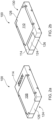
- Figure 2a shows that the mould material 114 partially covers and comprises a portion of the top major surface of the semiconductor device 100.
- the remaining portion of the top major surface comprises an exposed upper surface of the die attach portion 116 of the first lead frame 108.
- the exposed surface of the die attach portion 116 is obverse the side to which the semiconductor die is attached.
- Figure 2b shows that the mould material 114 partially covers and comprises a portion of the bottom major surface of the semiconductor device 100.
- the remaining portion of the bottom major surface comprises an exposed lower surface of the die attach portion 120 of the second lead frame 110.
- the exposed surface of the die attach portion 120 is obverse the side to which the semiconductor die is attached.
- This arrangement of exposed surfaces of the first lead frame 108 and the second lead frame 110 provides improved thermal dissipation of heat generated in the semiconductor die 102 during operation, whilst also allowing for electrical connection of the semiconductor device 100 to a carrier.
- the semiconductor device 100 is fixedly mounted and connected to the carrier by, for example, soldering the bottom contact surface 128, and a side contact surface 130 of the second lead frame to a corresponding connection on the carrier.
- the bottom and side contact surfaces 124, 126 of the first lead frame may be fixedly connected to a corresponding connection on the carrier.
- the side contact surface 130 of the second lead frame, as illustrated in Figure 1 extends partially upward on a side wall of the semiconductor device. This can be seen in Figure 2a which shows an absence bottom surface contact corresponding to the side contact surface 130 of the second lead frame.
- the exposed arrangement of the die attach portions 116, 120 through the mould material provide for improved heat dissipation whilst maintaining consistent bond line thickness across the area of the adhesive bond lines connecting the die attach portions of the respective first and second lead frames to the respective contact terminals 104, 106 of the semiconductor die 102.
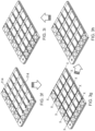
- Figures 3a to 3i show an example process steps for a method of making a semiconductor device according to an embodiment. The method can allow for a plurality of devices to be made.
- the method involves providing a plurality of connected second lead frames 110 arranged as a matrix.
- the second lead frames 110 are be suitably dimensioned for mounting a semiconductor die thereon.
- a suitable electrically conductive die attach material 112 is then provided on the second lead frames 110.
- the electrically conductive die attach material 112 may be a solder or conductive adhesive and may be dispensed on the second lead frames 110 by, for example stencil printing.
- the electrically conductive die attach material 112 allows for the electrical and mechanical of connection second contact terminal 106 of the semiconductor dies 102 to the second lead frames 110.
- the semiconductor dies are then placed on the conductive die attach material 112 arranged on the second lead frames 110.
- a further electrically conductive die attach material 112 is then provided by, for example stencil printing, on the first contact terminals 104 of the semiconductor dies 102 as illustrated in Figure 3d .
- the further electrically conductive die attach material 112 may be the same material as used in the die attach step discussed above with respect to Figure 3c and may be printed using a similar method.
- the first lead frames 108 are then mounted on the semiconductor die as shown in Figure 3e .
- the arrangement as assembled in Figure 3e is then placed within a clamp shell (not illustrated).
- the clamp shell may comprise a top portion which contacts the first lead frame 108, and a bottom portion which contacts the second lead frame 110.
- Locator or guide pins may be arranged on the top or bottom clamp, with corresponding holes on the first lead frames 108 and second lead frames 110, for receiving the locator pins, arranged on the top or bottom clamp. This holds the clamp in place prevents the lead frames, top and bottom portions of the clamp from becoming skewed during the reflow process.
- the clamping process also assist in maintaining the consistent bond line thickness mentioned above.
- the clamping process may be suitable for bulk bonding technique.
- the arrangement, as formed thus far, may then undergo solder reflow to make the electrical and mechanical connection of the lead frames 108, 110 to the respective contact terminals 104, 106 of the semiconductor dies 102.
- the conductive die attach material 112 is an adhesive
- the reflow process may be an adhesive curing process.
- the first lead frames 108 may also be arranged as a matrix. The first lead frames 108 are be suitably dimensioned for mounting to the semiconductor die 102.
- the process then continues at Figure 3f , where the arrangement undergoes encapsulation (or moulding) in an encapsulant 114 which fills the space around the substrates around the semiconductor die 102.
- the encapsulation process may be any suitable process such as mould mapping with film assisted moulding (FAM) provided that it results in the exposed surfaces of the lead frames as described above with respect to Figure 1 .
- FAM film assisted moulding
- the matrix arrangement undergoes a first series of cuts (indicated by lines x-x) along the side wall of the devices to expose the side contact surfaces 126, 130 of the first and second lead frames 108, 110.
- This exposure of the side contact surfaces 126, 130 allows for plating of the contact surfaces in Figure 3h .
- the matrix arrangement undergoes a second series of cuts, orthogonal to the first series of cuts, to singulate the semiconductor devices 100 according to embodiments and thus arriving at the individual device as shown in Figures 1 , 2a and 2b .
- the semiconductor device provides exposed heat sink portions on both sides of the device, whilst also allowing for soldering to a carrier such as PCB in which the solder joint is visible from the sides of the device.
Landscapes
- Lead Frames For Integrated Circuits (AREA)
- Engineering & Computer Science (AREA)
- Microelectronics & Electronic Packaging (AREA)
- Physics & Mathematics (AREA)
- Geometry (AREA)
- Ceramic Engineering (AREA)
Claims (5)
- Halbleiterbauelement (100), umfassend:ein Halbleiter-Die (102), wobei das Halbleiter-Die eine erste Hauptfläche mit einem daran angeordneten ersten Kontaktanschluss (104) und eine entgegengesetzte zweite Hauptfläche mit einem daran angeordneten zweiten Kontaktanschluss (106) umfasst;einen ersten Anschlussrahmen (108) mit einer ersten und einer zweiten Hauptfläche, die einander entgegengesetzt sind, wobei die erste Hauptfläche fest an dem ersten Kontaktanschluss des Halbleiter-Dies (102) angebracht ist;einen zweiten Anschlussrahmen (110) mit einer ersten und einer zweiten Hauptfläche, die einander entgegengesetzt sind, wobei die erste Hauptfläche fest an dem zweiten Kontaktanschluss des Halbleiter-Dies (102) angebracht ist;ein Formmaterial (114), das zum Einkapseln des Halbeiter-Dies (102) ausgeführt und angeordnet ist,wobei der erste Anschlussrahmen (108) einen angeformten äußeren Kontaktteil umfasst, der sich von seiner ersten Hauptfläche zu einer Ebene erstreckt, die mit der zweiten Hauptfläche des zweiten Anschlussrahmens (110) komplanar ist,wobei der erste und der zweite Anschlussrahmen (108, 110) ein erster bzw. zweiter Kühlkörper sind, die so ausgeführt und angeordnet sind, dass jeweilige zweite Hauptflächen durch das Formmaterial (114) an jeweiligen ersten und zweiten Hauptflächen des Halbleiterbauelements (102) freiliegen;wobei die zweite Hauptfläche des ersten Anschlussrahmens (108) mit dem Formmaterial (114) an den ersten Hauptflächen des Halbleiterbauelements (102) komplanar ist;wobei die zweite Hauptfläche des zweiten Anschlussrahmens (110) mit dem Formmaterial (114) an der zweiten Hauptfläche des Halbleiterbauelements komplanar ist;wobei der angeformte äußere Kontaktteil des ersten Anschlussrahmens (108) sich entlang einer Länge einer Seitenwand von der ersten zur zweiten Hauptfläche des Halbleiterbauelements (100) erstreckt;wobei der erste und der zweite Anschlussrahmen (108, 110) einen L-förmigen Querschnitt haben, dadurch gekennzeichnet, dassder zweite Anschlussrahmen (110) einen angeformten äußeren Kontaktteil umfasst, der sich teilweise entlang einer Länge einer Seitenwand von der zweiten Hauptfläche in Richtung auf die erste Hauptfläche of the Halbleiterbauelements (102) erstreckt;wobei die Länge des äußeren Kontaktteils des ersten Anschlussrahmens (108) größer als die Länge des äußeren Kontaktteils des zweiten Anschlussrahmens (110) ist.
- Halbleiterbauelement nach Anspruch 1, wobei die angeformten äußeren Kontaktteile als Kontaktteile angeordnet sind, die zum festen Montieren an einer Trägerfläche ausgeführt und angeordnet sind.
- Halbleiterbauelement nach einem der vorhergehenden Ansprüche, ferner umfassend: eine erste Schicht aus leitfähigem Klebstoff, die zwischen dem ersten Kontaktanschluss und der ersten Hauptfläche des ersten Anschlussrahmens angeordnet ist; und eine zweite Schicht aus leitfähigem Klebstoff, die zwischen dem zweiten Kontaktanschluss und der ersten Hauptfläche des zweiten Anschlussrahmens angeordnet ist.
- Halbleiterbauelement nach Anspruch 3, wobei eine Dicke der ersten Schicht aus leitfähigem Klebstoff über einen Kontaktbereich zwischen dem ersten Kontaktanschluss und der ersten Hauptfläche des ersten Anschlussrahmens gleichmäßig ist und eine Dicke der zweiten Schicht aus leitfähigem Klebstoff über einen Kontaktbereich zwischen dem zweiten Kontaktanschluss und der ersten Hauptfläche des zweiten Anschlussrahmens gleichmäßig ist.
- Verfahren zur Herstellung eines Halbleiterbauelements nach Ansprüchen 1 bis 4, wobei das Verfahren Folgendes umfasst:Bereitstellen eines Halbleiter-Dies, wobei das Halbleiter-Die eine erste Hauptfläche mit einem daran angeordneten ersten Kontaktanschluss und eine entgegengesetzte zweite Hauptfläche mit einem daran angeordneten zweiten Kontaktanschluss umfasst;Bereitstellen eines ersten Anschlussrahmens mit einer ersten und einer zweiten Hauptfläche, die einander entgegengesetzt sind, wobei die erste Hauptfläche fest an dem ersten Kontaktanschluss des Halbleiter-Dies angebracht ist;Bereitstellen eines zweiten Anschlussrahmens mit einer ersten und einer zweiten Hauptfläche, die einander entgegengesetzt sind, wobei die erste Hauptfläche fest an dem zweiten Kontaktanschluss des Halbleiter-Dies angebracht ist;wobei der erste Anschlussrahmen einen angeformten äußeren Kontaktteil umfasst, der sich von seiner ersten Hauptfläche zu einer Ebene erstreckt, die mit der zweiten Hauptfläche des zweiten Anschlussrahmens komplanar ist, undwobei der erste und der zweite Anschlussrahmen ein erster bzw. zweiter Kühlkörper sind, die so bereitgestellt sind, dass jeweilige zweite Hauptflächen durch ein Formmaterial an jeweiligen ersten und zweiten Hauptflächen des Halbleiterbauelements freiliegen;wobei die zweite Hauptfläche des ersten Anschlussrahmens so bereitgestellt ist, dass sie mit dem Formmaterial an den ersten Hauptflächen des Halbleiterbauelements komplanar ist.
Priority Applications (3)
| Application Number | Priority Date | Filing Date | Title |
|---|---|---|---|
| EP19156433.5A EP3693992B1 (de) | 2019-02-11 | 2019-02-11 | Oberflächenmontiertes halbleiterbauelement und verfahren zur herstellung |
| CN202010084999.8A CN111554651B (zh) | 2019-02-11 | 2020-02-10 | 表面安装半导体器件及其制造方法 |
| US16/787,221 US11233003B2 (en) | 2019-02-11 | 2020-02-11 | Surface mount semiconductor device with a plurality of lead frames |
Applications Claiming Priority (1)
| Application Number | Priority Date | Filing Date | Title |
|---|---|---|---|
| EP19156433.5A EP3693992B1 (de) | 2019-02-11 | 2019-02-11 | Oberflächenmontiertes halbleiterbauelement und verfahren zur herstellung |
Publications (2)
| Publication Number | Publication Date |
|---|---|
| EP3693992A1 EP3693992A1 (de) | 2020-08-12 |
| EP3693992B1 true EP3693992B1 (de) | 2024-08-07 |
Family
ID=65411759
Family Applications (1)
| Application Number | Title | Priority Date | Filing Date |
|---|---|---|---|
| EP19156433.5A Active EP3693992B1 (de) | 2019-02-11 | 2019-02-11 | Oberflächenmontiertes halbleiterbauelement und verfahren zur herstellung |
Country Status (3)
| Country | Link |
|---|---|
| US (1) | US11233003B2 (de) |
| EP (1) | EP3693992B1 (de) |
| CN (1) | CN111554651B (de) |
Families Citing this family (1)
| Publication number | Priority date | Publication date | Assignee | Title |
|---|---|---|---|---|
| JP2023055205A (ja) * | 2021-10-05 | 2023-04-17 | 住友電工デバイス・イノベーション株式会社 | 半導体デバイス及び半導体デバイスの製造方法 |
Family Cites Families (6)
| Publication number | Priority date | Publication date | Assignee | Title |
|---|---|---|---|---|
| US20060131734A1 (en) * | 2004-12-17 | 2006-06-22 | Texas Instruments Incorporated | Multi lead frame power package |
| US7495323B2 (en) * | 2006-08-30 | 2009-02-24 | Semiconductor Components Industries, L.L.C. | Semiconductor package structure having multiple heat dissipation paths and method of manufacture |
| US8193618B2 (en) * | 2008-12-12 | 2012-06-05 | Fairchild Semiconductor Corporation | Semiconductor die package with clip interconnection |
| US7816784B2 (en) * | 2008-12-17 | 2010-10-19 | Fairchild Semiconductor Corporation | Power quad flat no-lead semiconductor die packages with isolated heat sink for high-voltage, high-power applications, systems using the same, and methods of making the same |
| JP2015144216A (ja) * | 2014-01-31 | 2015-08-06 | 株式会社東芝 | 半導体装置及びその製造方法 |
| US9508625B2 (en) * | 2014-04-01 | 2016-11-29 | Infineon Technologies Ag | Semiconductor die package with multiple mounting configurations |
-
2019
- 2019-02-11 EP EP19156433.5A patent/EP3693992B1/de active Active
-
2020
- 2020-02-10 CN CN202010084999.8A patent/CN111554651B/zh active Active
- 2020-02-11 US US16/787,221 patent/US11233003B2/en active Active
Also Published As
| Publication number | Publication date |
|---|---|
| EP3693992A1 (de) | 2020-08-12 |
| CN111554651A (zh) | 2020-08-18 |
| US11233003B2 (en) | 2022-01-25 |
| US20200258829A1 (en) | 2020-08-13 |
| CN111554651B (zh) | 2025-09-16 |
Similar Documents
| Publication | Publication Date | Title |
|---|---|---|
| US7768105B2 (en) | Pre-molded clip structure | |
| US8728929B2 (en) | Pre-soldered leadless package | |
| US5299091A (en) | Packaged semiconductor device having heat dissipation/electrical connection bumps and method of manufacturing same | |
| EP3817033B1 (de) | Halbleiterpaket und herstellungsverfahren dafür | |
| US7498195B2 (en) | Multi-chip semiconductor connector assembly method | |
| US11227820B2 (en) | Through hole side wettable flank | |
| EP3982405A1 (de) | Halbleitergehäuse mit erhöhter zuverlässigkeit auf leiterplattenebene | |
| EP0623954B1 (de) | Vergossene Kunststoffverkapselung für elektronische Anordnungen | |
| EP0978871A2 (de) | Ein Packungsentwurf für eine Anordnung niedriger Leistung | |
| US11233003B2 (en) | Surface mount semiconductor device with a plurality of lead frames | |
| JP2801810B2 (ja) | 樹脂封止型半導体装置 | |
| WO2008091919A2 (en) | Thermally enhanced single in-line package (sip) | |
| EP4657521A1 (de) | Verfahren zur herstellung einer halbleiterpackung für integrierte schaltungen | |
| JPWO1999056313A1 (ja) | 半導体装置およびその製造方法 | |
| US20230402355A1 (en) | Electronic package with heatsink and manufacturing method therefor | |
| US20230027138A1 (en) | Power module | |
| EP4123699A1 (de) | Halbleiterbauelement und verfahren zur herstellung eines halbleiterbauelements | |
| JPH07326690A (ja) | 半導体装置用パッケージおよび半導体装置 | |
| JP5261025B2 (ja) | 樹脂封止型半導体装置及び樹脂封止型半導体装置の製造方法 | |
| JPH06163760A (ja) | 放熱スラグを有した電子部品搭載用基板 | |
| Hundt | High power surface mount packages | |
| US20090001533A1 (en) | Multi-chip packaging in a tsop package | |
| JPH0590439A (ja) | ベアチツプリードレスパツケージ | |
| JPH06163632A (ja) | 半導体装置 |
Legal Events
| Date | Code | Title | Description |
|---|---|---|---|
| PUAI | Public reference made under article 153(3) epc to a published international application that has entered the european phase |
Free format text: ORIGINAL CODE: 0009012 |
|
| STAA | Information on the status of an ep patent application or granted ep patent |
Free format text: STATUS: THE APPLICATION HAS BEEN PUBLISHED |
|
| AK | Designated contracting states |
Kind code of ref document: A1 Designated state(s): AL AT BE BG CH CY CZ DE DK EE ES FI FR GB GR HR HU IE IS IT LI LT LU LV MC MK MT NL NO PL PT RO RS SE SI SK SM TR |
|
| AX | Request for extension of the european patent |
Extension state: BA ME |
|
| STAA | Information on the status of an ep patent application or granted ep patent |
Free format text: STATUS: REQUEST FOR EXAMINATION WAS MADE |
|
| 17P | Request for examination filed |
Effective date: 20210210 |
|
| RBV | Designated contracting states (corrected) |
Designated state(s): AL AT BE BG CH CY CZ DE DK EE ES FI FR GB GR HR HU IE IS IT LI LT LU LV MC MK MT NL NO PL PT RO RS SE SI SK SM TR |
|
| STAA | Information on the status of an ep patent application or granted ep patent |
Free format text: STATUS: EXAMINATION IS IN PROGRESS |
|
| 17Q | First examination report despatched |
Effective date: 20210428 |
|
| GRAP | Despatch of communication of intention to grant a patent |
Free format text: ORIGINAL CODE: EPIDOSNIGR1 |
|
| STAA | Information on the status of an ep patent application or granted ep patent |
Free format text: STATUS: GRANT OF PATENT IS INTENDED |
|
| INTG | Intention to grant announced |
Effective date: 20240426 |
|
| RIN1 | Information on inventor provided before grant (corrected) |
Inventor name: HUNG, MELVIN Inventor name: RAMALINGAM, VEGNESWARY Inventor name: TING, CHRISTINE |
|
| GRAS | Grant fee paid |
Free format text: ORIGINAL CODE: EPIDOSNIGR3 |
|
| GRAA | (expected) grant |
Free format text: ORIGINAL CODE: 0009210 |
|
| STAA | Information on the status of an ep patent application or granted ep patent |
Free format text: STATUS: THE PATENT HAS BEEN GRANTED |
|
| AK | Designated contracting states |
Kind code of ref document: B1 Designated state(s): AL AT BE BG CH CY CZ DE DK EE ES FI FR GB GR HR HU IE IS IT LI LT LU LV MC MK MT NL NO PL PT RO RS SE SI SK SM TR |
|
| REG | Reference to a national code |
Ref country code: GB Ref legal event code: FG4D |
|
| REG | Reference to a national code |
Ref country code: CH Ref legal event code: EP |
|
| REG | Reference to a national code |
Ref country code: IE Ref legal event code: FG4D |
|
| REG | Reference to a national code |
Ref country code: DE Ref legal event code: R096 Ref document number: 602019056429 Country of ref document: DE |
|
| REG | Reference to a national code |
Ref country code: LT Ref legal event code: MG9D |
|
| REG | Reference to a national code |
Ref country code: NL Ref legal event code: MP Effective date: 20240807 |
|
| PG25 | Lapsed in a contracting state [announced via postgrant information from national office to epo] |
Ref country code: NO Free format text: LAPSE BECAUSE OF FAILURE TO SUBMIT A TRANSLATION OF THE DESCRIPTION OR TO PAY THE FEE WITHIN THE PRESCRIBED TIME-LIMIT Effective date: 20241107 |
|
| REG | Reference to a national code |
Ref country code: AT Ref legal event code: MK05 Ref document number: 1711935 Country of ref document: AT Kind code of ref document: T Effective date: 20240807 |
|
| PG25 | Lapsed in a contracting state [announced via postgrant information from national office to epo] |
Ref country code: NL Free format text: LAPSE BECAUSE OF FAILURE TO SUBMIT A TRANSLATION OF THE DESCRIPTION OR TO PAY THE FEE WITHIN THE PRESCRIBED TIME-LIMIT Effective date: 20240807 Ref country code: FI Free format text: LAPSE BECAUSE OF FAILURE TO SUBMIT A TRANSLATION OF THE DESCRIPTION OR TO PAY THE FEE WITHIN THE PRESCRIBED TIME-LIMIT Effective date: 20240807 Ref country code: PL Free format text: LAPSE BECAUSE OF FAILURE TO SUBMIT A TRANSLATION OF THE DESCRIPTION OR TO PAY THE FEE WITHIN THE PRESCRIBED TIME-LIMIT Effective date: 20240807 Ref country code: GR Free format text: LAPSE BECAUSE OF FAILURE TO SUBMIT A TRANSLATION OF THE DESCRIPTION OR TO PAY THE FEE WITHIN THE PRESCRIBED TIME-LIMIT Effective date: 20241108 Ref country code: PT Free format text: LAPSE BECAUSE OF FAILURE TO SUBMIT A TRANSLATION OF THE DESCRIPTION OR TO PAY THE FEE WITHIN THE PRESCRIBED TIME-LIMIT Effective date: 20241209 |
|
| PG25 | Lapsed in a contracting state [announced via postgrant information from national office to epo] |
Ref country code: BG Free format text: LAPSE BECAUSE OF FAILURE TO SUBMIT A TRANSLATION OF THE DESCRIPTION OR TO PAY THE FEE WITHIN THE PRESCRIBED TIME-LIMIT Effective date: 20240807 |
|
| PG25 | Lapsed in a contracting state [announced via postgrant information from national office to epo] |
Ref country code: LV Free format text: LAPSE BECAUSE OF FAILURE TO SUBMIT A TRANSLATION OF THE DESCRIPTION OR TO PAY THE FEE WITHIN THE PRESCRIBED TIME-LIMIT Effective date: 20240807 |
|
| PG25 | Lapsed in a contracting state [announced via postgrant information from national office to epo] |
Ref country code: AT Free format text: LAPSE BECAUSE OF FAILURE TO SUBMIT A TRANSLATION OF THE DESCRIPTION OR TO PAY THE FEE WITHIN THE PRESCRIBED TIME-LIMIT Effective date: 20240807 Ref country code: IS Free format text: LAPSE BECAUSE OF FAILURE TO SUBMIT A TRANSLATION OF THE DESCRIPTION OR TO PAY THE FEE WITHIN THE PRESCRIBED TIME-LIMIT Effective date: 20241207 |
|
| PG25 | Lapsed in a contracting state [announced via postgrant information from national office to epo] |
Ref country code: HR Free format text: LAPSE BECAUSE OF FAILURE TO SUBMIT A TRANSLATION OF THE DESCRIPTION OR TO PAY THE FEE WITHIN THE PRESCRIBED TIME-LIMIT Effective date: 20240807 |
|
| PG25 | Lapsed in a contracting state [announced via postgrant information from national office to epo] |
Ref country code: ES Free format text: LAPSE BECAUSE OF FAILURE TO SUBMIT A TRANSLATION OF THE DESCRIPTION OR TO PAY THE FEE WITHIN THE PRESCRIBED TIME-LIMIT Effective date: 20240807 Ref country code: RS Free format text: LAPSE BECAUSE OF FAILURE TO SUBMIT A TRANSLATION OF THE DESCRIPTION OR TO PAY THE FEE WITHIN THE PRESCRIBED TIME-LIMIT Effective date: 20241107 |
|
| PG25 | Lapsed in a contracting state [announced via postgrant information from national office to epo] |
Ref country code: RS Free format text: LAPSE BECAUSE OF FAILURE TO SUBMIT A TRANSLATION OF THE DESCRIPTION OR TO PAY THE FEE WITHIN THE PRESCRIBED TIME-LIMIT Effective date: 20241107 Ref country code: PT Free format text: LAPSE BECAUSE OF FAILURE TO SUBMIT A TRANSLATION OF THE DESCRIPTION OR TO PAY THE FEE WITHIN THE PRESCRIBED TIME-LIMIT Effective date: 20241209 Ref country code: PL Free format text: LAPSE BECAUSE OF FAILURE TO SUBMIT A TRANSLATION OF THE DESCRIPTION OR TO PAY THE FEE WITHIN THE PRESCRIBED TIME-LIMIT Effective date: 20240807 Ref country code: NO Free format text: LAPSE BECAUSE OF FAILURE TO SUBMIT A TRANSLATION OF THE DESCRIPTION OR TO PAY THE FEE WITHIN THE PRESCRIBED TIME-LIMIT Effective date: 20241107 Ref country code: NL Free format text: LAPSE BECAUSE OF FAILURE TO SUBMIT A TRANSLATION OF THE DESCRIPTION OR TO PAY THE FEE WITHIN THE PRESCRIBED TIME-LIMIT Effective date: 20240807 Ref country code: LV Free format text: LAPSE BECAUSE OF FAILURE TO SUBMIT A TRANSLATION OF THE DESCRIPTION OR TO PAY THE FEE WITHIN THE PRESCRIBED TIME-LIMIT Effective date: 20240807 Ref country code: IS Free format text: LAPSE BECAUSE OF FAILURE TO SUBMIT A TRANSLATION OF THE DESCRIPTION OR TO PAY THE FEE WITHIN THE PRESCRIBED TIME-LIMIT Effective date: 20241207 Ref country code: HR Free format text: LAPSE BECAUSE OF FAILURE TO SUBMIT A TRANSLATION OF THE DESCRIPTION OR TO PAY THE FEE WITHIN THE PRESCRIBED TIME-LIMIT Effective date: 20240807 Ref country code: GR Free format text: LAPSE BECAUSE OF FAILURE TO SUBMIT A TRANSLATION OF THE DESCRIPTION OR TO PAY THE FEE WITHIN THE PRESCRIBED TIME-LIMIT Effective date: 20241108 Ref country code: FI Free format text: LAPSE BECAUSE OF FAILURE TO SUBMIT A TRANSLATION OF THE DESCRIPTION OR TO PAY THE FEE WITHIN THE PRESCRIBED TIME-LIMIT Effective date: 20240807 Ref country code: ES Free format text: LAPSE BECAUSE OF FAILURE TO SUBMIT A TRANSLATION OF THE DESCRIPTION OR TO PAY THE FEE WITHIN THE PRESCRIBED TIME-LIMIT Effective date: 20240807 Ref country code: BG Free format text: LAPSE BECAUSE OF FAILURE TO SUBMIT A TRANSLATION OF THE DESCRIPTION OR TO PAY THE FEE WITHIN THE PRESCRIBED TIME-LIMIT Effective date: 20240807 Ref country code: AT Free format text: LAPSE BECAUSE OF FAILURE TO SUBMIT A TRANSLATION OF THE DESCRIPTION OR TO PAY THE FEE WITHIN THE PRESCRIBED TIME-LIMIT Effective date: 20240807 |
|
| PG25 | Lapsed in a contracting state [announced via postgrant information from national office to epo] |
Ref country code: DK Free format text: LAPSE BECAUSE OF FAILURE TO SUBMIT A TRANSLATION OF THE DESCRIPTION OR TO PAY THE FEE WITHIN THE PRESCRIBED TIME-LIMIT Effective date: 20240807 Ref country code: RO Free format text: LAPSE BECAUSE OF FAILURE TO SUBMIT A TRANSLATION OF THE DESCRIPTION OR TO PAY THE FEE WITHIN THE PRESCRIBED TIME-LIMIT Effective date: 20240807 Ref country code: SM Free format text: LAPSE BECAUSE OF FAILURE TO SUBMIT A TRANSLATION OF THE DESCRIPTION OR TO PAY THE FEE WITHIN THE PRESCRIBED TIME-LIMIT Effective date: 20240807 |
|
| PG25 | Lapsed in a contracting state [announced via postgrant information from national office to epo] |
Ref country code: EE Free format text: LAPSE BECAUSE OF FAILURE TO SUBMIT A TRANSLATION OF THE DESCRIPTION OR TO PAY THE FEE WITHIN THE PRESCRIBED TIME-LIMIT Effective date: 20240807 |
|
| PG25 | Lapsed in a contracting state [announced via postgrant information from national office to epo] |
Ref country code: CZ Free format text: LAPSE BECAUSE OF FAILURE TO SUBMIT A TRANSLATION OF THE DESCRIPTION OR TO PAY THE FEE WITHIN THE PRESCRIBED TIME-LIMIT Effective date: 20240807 |
|
| PG25 | Lapsed in a contracting state [announced via postgrant information from national office to epo] |
Ref country code: SK Free format text: LAPSE BECAUSE OF FAILURE TO SUBMIT A TRANSLATION OF THE DESCRIPTION OR TO PAY THE FEE WITHIN THE PRESCRIBED TIME-LIMIT Effective date: 20240807 |
|
| REG | Reference to a national code |
Ref country code: DE Ref legal event code: R097 Ref document number: 602019056429 Country of ref document: DE |
|
| PLBE | No opposition filed within time limit |
Free format text: ORIGINAL CODE: 0009261 |
|
| STAA | Information on the status of an ep patent application or granted ep patent |
Free format text: STATUS: NO OPPOSITION FILED WITHIN TIME LIMIT |
|
| 26N | No opposition filed |
Effective date: 20250508 |
|
| PG25 | Lapsed in a contracting state [announced via postgrant information from national office to epo] |
Ref country code: SE Free format text: LAPSE BECAUSE OF FAILURE TO SUBMIT A TRANSLATION OF THE DESCRIPTION OR TO PAY THE FEE WITHIN THE PRESCRIBED TIME-LIMIT Effective date: 20240807 |
|
| PG25 | Lapsed in a contracting state [announced via postgrant information from national office to epo] |
Ref country code: MC Free format text: LAPSE BECAUSE OF FAILURE TO SUBMIT A TRANSLATION OF THE DESCRIPTION OR TO PAY THE FEE WITHIN THE PRESCRIBED TIME-LIMIT Effective date: 20240807 |
|
| REG | Reference to a national code |
Ref country code: CH Ref legal event code: PL |
|
| PG25 | Lapsed in a contracting state [announced via postgrant information from national office to epo] |
Ref country code: LU Free format text: LAPSE BECAUSE OF NON-PAYMENT OF DUE FEES Effective date: 20250211 |
|
| PG25 | Lapsed in a contracting state [announced via postgrant information from national office to epo] |
Ref country code: CH Free format text: LAPSE BECAUSE OF NON-PAYMENT OF DUE FEES Effective date: 20250228 |
|
| GBPC | Gb: european patent ceased through non-payment of renewal fee |
Effective date: 20250211 |
|
| REG | Reference to a national code |
Ref country code: DE Ref legal event code: R079 Ref document number: 602019056429 Country of ref document: DE Free format text: PREVIOUS MAIN CLASS: H01L0023495000 Ipc: H10W0070400000 |
|
| REG | Reference to a national code |
Ref country code: BE Ref legal event code: MM Effective date: 20250228 |
|
| PG25 | Lapsed in a contracting state [announced via postgrant information from national office to epo] |
Ref country code: GB Free format text: LAPSE BECAUSE OF NON-PAYMENT OF DUE FEES Effective date: 20250211 |
|
| PG25 | Lapsed in a contracting state [announced via postgrant information from national office to epo] |
Ref country code: FR Free format text: LAPSE BECAUSE OF NON-PAYMENT OF DUE FEES Effective date: 20250228 |
|
| PG25 | Lapsed in a contracting state [announced via postgrant information from national office to epo] |
Ref country code: BE Free format text: LAPSE BECAUSE OF NON-PAYMENT OF DUE FEES Effective date: 20250228 |
|
| PG25 | Lapsed in a contracting state [announced via postgrant information from national office to epo] |
Ref country code: IE Free format text: LAPSE BECAUSE OF NON-PAYMENT OF DUE FEES Effective date: 20250211 |
|
| PG25 | Lapsed in a contracting state [announced via postgrant information from national office to epo] |
Ref country code: IT Free format text: LAPSE BECAUSE OF FAILURE TO SUBMIT A TRANSLATION OF THE DESCRIPTION OR TO PAY THE FEE WITHIN THE PRESCRIBED TIME-LIMIT Effective date: 20240807 |
|
| PGFP | Annual fee paid to national office [announced via postgrant information from national office to epo] |
Ref country code: DE Payment date: 20260220 Year of fee payment: 8 |