EP3707746B1 - Gaszufuhrsystem für hochdruckprozesskammer - Google Patents
Gaszufuhrsystem für hochdruckprozesskammer Download PDFInfo
- Publication number
- EP3707746B1 EP3707746B1 EP18876650.5A EP18876650A EP3707746B1 EP 3707746 B1 EP3707746 B1 EP 3707746B1 EP 18876650 A EP18876650 A EP 18876650A EP 3707746 B1 EP3707746 B1 EP 3707746B1
- Authority
- EP
- European Patent Office
- Prior art keywords
- chamber
- pressure
- gas
- gas delivery
- delivery module
- Prior art date
- Legal status (The legal status is an assumption and is not a legal conclusion. Google has not performed a legal analysis and makes no representation as to the accuracy of the status listed.)
- Active
Links
Images



Classifications
-
- H—ELECTRICITY
- H10—SEMICONDUCTOR DEVICES; ELECTRIC SOLID-STATE DEVICES NOT OTHERWISE PROVIDED FOR
- H10P—GENERIC PROCESSES OR APPARATUS FOR THE MANUFACTURE OR TREATMENT OF DEVICES COVERED BY CLASS H10
- H10P72/00—Handling or holding of wafers, substrates or devices during manufacture or treatment thereof
- H10P72/04—Apparatus for manufacture or treatment
- H10P72/0402—Apparatus for fluid treatment
-
- C—CHEMISTRY; METALLURGY
- C23—COATING METALLIC MATERIAL; COATING MATERIAL WITH METALLIC MATERIAL; CHEMICAL SURFACE TREATMENT; DIFFUSION TREATMENT OF METALLIC MATERIAL; COATING BY VACUUM EVAPORATION, BY SPUTTERING, BY ION IMPLANTATION OR BY CHEMICAL VAPOUR DEPOSITION, IN GENERAL; INHIBITING CORROSION OF METALLIC MATERIAL OR INCRUSTATION IN GENERAL
- C23C—COATING METALLIC MATERIAL; COATING MATERIAL WITH METALLIC MATERIAL; SURFACE TREATMENT OF METALLIC MATERIAL BY DIFFUSION INTO THE SURFACE, BY CHEMICAL CONVERSION OR SUBSTITUTION; COATING BY VACUUM EVAPORATION, BY SPUTTERING, BY ION IMPLANTATION OR BY CHEMICAL VAPOUR DEPOSITION, IN GENERAL
- C23C16/00—Chemical coating by decomposition of gaseous compounds, without leaving reaction products of surface material in the coating, i.e. chemical vapour deposition [CVD] processes
- C23C16/44—Chemical coating by decomposition of gaseous compounds, without leaving reaction products of surface material in the coating, i.e. chemical vapour deposition [CVD] processes characterised by the method of coating
- C23C16/4412—Details relating to the exhausts, e.g. pumps, filters, scrubbers, particle traps
-
- C—CHEMISTRY; METALLURGY
- C23—COATING METALLIC MATERIAL; COATING MATERIAL WITH METALLIC MATERIAL; CHEMICAL SURFACE TREATMENT; DIFFUSION TREATMENT OF METALLIC MATERIAL; COATING BY VACUUM EVAPORATION, BY SPUTTERING, BY ION IMPLANTATION OR BY CHEMICAL VAPOUR DEPOSITION, IN GENERAL; INHIBITING CORROSION OF METALLIC MATERIAL OR INCRUSTATION IN GENERAL
- C23C—COATING METALLIC MATERIAL; COATING MATERIAL WITH METALLIC MATERIAL; SURFACE TREATMENT OF METALLIC MATERIAL BY DIFFUSION INTO THE SURFACE, BY CHEMICAL CONVERSION OR SUBSTITUTION; COATING BY VACUUM EVAPORATION, BY SPUTTERING, BY ION IMPLANTATION OR BY CHEMICAL VAPOUR DEPOSITION, IN GENERAL
- C23C16/00—Chemical coating by decomposition of gaseous compounds, without leaving reaction products of surface material in the coating, i.e. chemical vapour deposition [CVD] processes
- C23C16/44—Chemical coating by decomposition of gaseous compounds, without leaving reaction products of surface material in the coating, i.e. chemical vapour deposition [CVD] processes characterised by the method of coating
- C23C16/455—Chemical coating by decomposition of gaseous compounds, without leaving reaction products of surface material in the coating, i.e. chemical vapour deposition [CVD] processes characterised by the method of coating characterised by the method used for introducing gases into reaction chamber or for modifying gas flows in reaction chamber
-
- C—CHEMISTRY; METALLURGY
- C23—COATING METALLIC MATERIAL; COATING MATERIAL WITH METALLIC MATERIAL; CHEMICAL SURFACE TREATMENT; DIFFUSION TREATMENT OF METALLIC MATERIAL; COATING BY VACUUM EVAPORATION, BY SPUTTERING, BY ION IMPLANTATION OR BY CHEMICAL VAPOUR DEPOSITION, IN GENERAL; INHIBITING CORROSION OF METALLIC MATERIAL OR INCRUSTATION IN GENERAL
- C23C—COATING METALLIC MATERIAL; COATING MATERIAL WITH METALLIC MATERIAL; SURFACE TREATMENT OF METALLIC MATERIAL BY DIFFUSION INTO THE SURFACE, BY CHEMICAL CONVERSION OR SUBSTITUTION; COATING BY VACUUM EVAPORATION, BY SPUTTERING, BY ION IMPLANTATION OR BY CHEMICAL VAPOUR DEPOSITION, IN GENERAL
- C23C16/00—Chemical coating by decomposition of gaseous compounds, without leaving reaction products of surface material in the coating, i.e. chemical vapour deposition [CVD] processes
- C23C16/44—Chemical coating by decomposition of gaseous compounds, without leaving reaction products of surface material in the coating, i.e. chemical vapour deposition [CVD] processes characterised by the method of coating
- C23C16/455—Chemical coating by decomposition of gaseous compounds, without leaving reaction products of surface material in the coating, i.e. chemical vapour deposition [CVD] processes characterised by the method of coating characterised by the method used for introducing gases into reaction chamber or for modifying gas flows in reaction chamber
- C23C16/45557—Pulsed pressure or control pressure
-
- H—ELECTRICITY
- H10—SEMICONDUCTOR DEVICES; ELECTRIC SOLID-STATE DEVICES NOT OTHERWISE PROVIDED FOR
- H10P—GENERIC PROCESSES OR APPARATUS FOR THE MANUFACTURE OR TREATMENT OF DEVICES COVERED BY CLASS H10
- H10P14/00—Formation of materials, e.g. in the shape of layers or pillars
- H10P14/60—Formation of materials, e.g. in the shape of layers or pillars of insulating materials
- H10P14/63—Formation of materials, e.g. in the shape of layers or pillars of insulating materials characterised by the formation processes
- H10P14/6326—Deposition processes
- H10P14/6328—Deposition from the gas or vapour phase
-
- H—ELECTRICITY
- H10—SEMICONDUCTOR DEVICES; ELECTRIC SOLID-STATE DEVICES NOT OTHERWISE PROVIDED FOR
- H10P—GENERIC PROCESSES OR APPARATUS FOR THE MANUFACTURE OR TREATMENT OF DEVICES COVERED BY CLASS H10
- H10P72/00—Handling or holding of wafers, substrates or devices during manufacture or treatment thereof
- H10P72/04—Apparatus for manufacture or treatment
- H10P72/0402—Apparatus for fluid treatment
- H10P72/0418—Apparatus for fluid treatment for etching
- H10P72/0421—Apparatus for fluid treatment for etching for drying etching
-
- H—ELECTRICITY
- H10—SEMICONDUCTOR DEVICES; ELECTRIC SOLID-STATE DEVICES NOT OTHERWISE PROVIDED FOR
- H10P—GENERIC PROCESSES OR APPARATUS FOR THE MANUFACTURE OR TREATMENT OF DEVICES COVERED BY CLASS H10
- H10P72/00—Handling or holding of wafers, substrates or devices during manufacture or treatment thereof
- H10P72/04—Apparatus for manufacture or treatment
- H10P72/0431—Apparatus for thermal treatment
-
- H—ELECTRICITY
- H10—SEMICONDUCTOR DEVICES; ELECTRIC SOLID-STATE DEVICES NOT OTHERWISE PROVIDED FOR
- H10P—GENERIC PROCESSES OR APPARATUS FOR THE MANUFACTURE OR TREATMENT OF DEVICES COVERED BY CLASS H10
- H10P72/00—Handling or holding of wafers, substrates or devices during manufacture or treatment thereof
- H10P72/04—Apparatus for manufacture or treatment
- H10P72/0431—Apparatus for thermal treatment
- H10P72/0434—Apparatus for thermal treatment mainly by convection
-
- H—ELECTRICITY
- H10—SEMICONDUCTOR DEVICES; ELECTRIC SOLID-STATE DEVICES NOT OTHERWISE PROVIDED FOR
- H10P—GENERIC PROCESSES OR APPARATUS FOR THE MANUFACTURE OR TREATMENT OF DEVICES COVERED BY CLASS H10
- H10P72/00—Handling or holding of wafers, substrates or devices during manufacture or treatment thereof
- H10P72/04—Apparatus for manufacture or treatment
- H10P72/0451—Apparatus for manufacturing or treating in a plurality of work-stations
- H10P72/0462—Apparatus for manufacturing or treating in a plurality of work-stations characterised by the construction of the processing chambers, e.g. modular processing chambers
-
- H—ELECTRICITY
- H10—SEMICONDUCTOR DEVICES; ELECTRIC SOLID-STATE DEVICES NOT OTHERWISE PROVIDED FOR
- H10P—GENERIC PROCESSES OR APPARATUS FOR THE MANUFACTURE OR TREATMENT OF DEVICES COVERED BY CLASS H10
- H10P72/00—Handling or holding of wafers, substrates or devices during manufacture or treatment thereof
- H10P72/04—Apparatus for manufacture or treatment
- H10P72/0451—Apparatus for manufacturing or treating in a plurality of work-stations
- H10P72/0464—Apparatus for manufacturing or treating in a plurality of work-stations characterised by the construction of the transfer chamber
-
- H—ELECTRICITY
- H10—SEMICONDUCTOR DEVICES; ELECTRIC SOLID-STATE DEVICES NOT OTHERWISE PROVIDED FOR
- H10P—GENERIC PROCESSES OR APPARATUS FOR THE MANUFACTURE OR TREATMENT OF DEVICES COVERED BY CLASS H10
- H10P72/00—Handling or holding of wafers, substrates or devices during manufacture or treatment thereof
- H10P72/04—Apparatus for manufacture or treatment
- H10P72/0451—Apparatus for manufacturing or treating in a plurality of work-stations
- H10P72/0466—Apparatus for manufacturing or treating in a plurality of work-stations characterised by the construction of the load-lock chamber
-
- H—ELECTRICITY
- H10—SEMICONDUCTOR DEVICES; ELECTRIC SOLID-STATE DEVICES NOT OTHERWISE PROVIDED FOR
- H10P—GENERIC PROCESSES OR APPARATUS FOR THE MANUFACTURE OR TREATMENT OF DEVICES COVERED BY CLASS H10
- H10P72/00—Handling or holding of wafers, substrates or devices during manufacture or treatment thereof
- H10P72/06—Apparatus for monitoring, sorting, marking, testing or measuring
- H10P72/0602—Temperature monitoring
-
- H—ELECTRICITY
- H10—SEMICONDUCTOR DEVICES; ELECTRIC SOLID-STATE DEVICES NOT OTHERWISE PROVIDED FOR
- H10P—GENERIC PROCESSES OR APPARATUS FOR THE MANUFACTURE OR TREATMENT OF DEVICES COVERED BY CLASS H10
- H10P72/00—Handling or holding of wafers, substrates or devices during manufacture or treatment thereof
- H10P72/06—Apparatus for monitoring, sorting, marking, testing or measuring
- H10P72/0604—Process monitoring, e.g. flow or thickness monitoring
-
- H—ELECTRICITY
- H10—SEMICONDUCTOR DEVICES; ELECTRIC SOLID-STATE DEVICES NOT OTHERWISE PROVIDED FOR
- H10P—GENERIC PROCESSES OR APPARATUS FOR THE MANUFACTURE OR TREATMENT OF DEVICES COVERED BY CLASS H10
- H10P72/00—Handling or holding of wafers, substrates or devices during manufacture or treatment thereof
- H10P72/30—Handling or holding of wafers, substrates or devices during manufacture or treatment thereof for conveying, e.g. between different workstations
- H10P72/33—Handling or holding of wafers, substrates or devices during manufacture or treatment thereof for conveying, e.g. between different workstations into and out of processing chamber
- H10P72/3304—Handling or holding of wafers, substrates or devices during manufacture or treatment thereof for conveying, e.g. between different workstations into and out of processing chamber characterised by movements or sequence of movements of transfer devices
-
- H—ELECTRICITY
- H10—SEMICONDUCTOR DEVICES; ELECTRIC SOLID-STATE DEVICES NOT OTHERWISE PROVIDED FOR
- H10P—GENERIC PROCESSES OR APPARATUS FOR THE MANUFACTURE OR TREATMENT OF DEVICES COVERED BY CLASS H10
- H10P72/00—Handling or holding of wafers, substrates or devices during manufacture or treatment thereof
- H10P72/30—Handling or holding of wafers, substrates or devices during manufacture or treatment thereof for conveying, e.g. between different workstations
- H10P72/33—Handling or holding of wafers, substrates or devices during manufacture or treatment thereof for conveying, e.g. between different workstations into and out of processing chamber
- H10P72/3306—Horizontal transfer of a single workpiece
-
- H—ELECTRICITY
- H10—SEMICONDUCTOR DEVICES; ELECTRIC SOLID-STATE DEVICES NOT OTHERWISE PROVIDED FOR
- H10P—GENERIC PROCESSES OR APPARATUS FOR THE MANUFACTURE OR TREATMENT OF DEVICES COVERED BY CLASS H10
- H10P74/00—Testing or measuring during manufacture or treatment of wafers, substrates or devices
- H10P74/23—Testing or measuring during manufacture or treatment of wafers, substrates or devices characterised by multiple measurements, corrections, marking or sorting processes
-
- H—ELECTRICITY
- H10—SEMICONDUCTOR DEVICES; ELECTRIC SOLID-STATE DEVICES NOT OTHERWISE PROVIDED FOR
- H10P—GENERIC PROCESSES OR APPARATUS FOR THE MANUFACTURE OR TREATMENT OF DEVICES COVERED BY CLASS H10
- H10P95/00—Generic processes or apparatus for manufacture or treatments not covered by the other groups of this subclass
- H10P95/90—Thermal treatments, e.g. annealing or sintering
-
- H—ELECTRICITY
- H10—SEMICONDUCTOR DEVICES; ELECTRIC SOLID-STATE DEVICES NOT OTHERWISE PROVIDED FOR
- H10P—GENERIC PROCESSES OR APPARATUS FOR THE MANUFACTURE OR TREATMENT OF DEVICES COVERED BY CLASS H10
- H10P72/00—Handling or holding of wafers, substrates or devices during manufacture or treatment thereof
- H10P72/04—Apparatus for manufacture or treatment
- H10P72/0451—Apparatus for manufacturing or treating in a plurality of work-stations
- H10P72/0452—Apparatus for manufacturing or treating in a plurality of work-stations characterised by the layout of the process chambers
- H10P72/0454—Apparatus for manufacturing or treating in a plurality of work-stations characterised by the layout of the process chambers surrounding a central transfer chamber
Definitions
- This invention relates to a high pressure processing chamber for integrated circuit fabrication.
- Micro-electronic circuits and other micro-scale devices are generally manufactured from a substrate, such as a silicon or other semiconductor material substrate. Multiple metal layers are applied onto the substrate to form microelectronic or other micro-scale components or to provide electrical connections. These metal layers, e.g., copper, are plated onto the substrate, and form the components and interconnects in a sequence of photolithographic, plating, etching, polishing, or other operations.
- a substrate such as a silicon or other semiconductor material substrate.
- Multiple metal layers are applied onto the substrate to form microelectronic or other micro-scale components or to provide electrical connections. These metal layers, e.g., copper, are plated onto the substrate, and form the components and interconnects in a sequence of photolithographic, plating, etching, polishing, or other operations.
- the substrate is typically put through an annealing process in which the substrate is quickly heated, usually to about 200-500°C.
- the substrate may be held at these temperatures for a relatively short time, e.g., 60-300 seconds.
- the substrate is then rapidly cooled, with the entire process usually taking only a few minutes.
- Annealing may be used to change the material properties of the layers on the substrate. It may also be used to activate dopants, drive dopants between films on the substrate, change film-to-film or film-to-substrate interfaces, densify deposited films, or to repair damage from ion implantation.
- a high-pressure processing system for processing a layer on a substrate.
- the system includes a first chamber, a support to hold the substrate in the first chamber, a second chamber adjacent the first chamber, a foreline to remove gas from the second chamber, a vacuum processing system configured to lower a pressure within the second chamber, a valve assembly between the first chamber and the second chamber to isolate the pressure within the first chamber from the pressure within the second chamber, a gas delivery system configured to introduce one or more gases into the first chamber and to increase the pressure within the first chamber to at least 7600 Torr (10 atmospheres) while the gas is in the first chamber and while the first chamber is isolated from the second chamber, a controller configured to operate the gas delivery system and the valve assembly, an exhaust system comprising an exhaust line to remove gas from the first chamber, and a common housing surrounding both the first gas delivery module and the second gas delivery module.
- the gas delivery system includes a first gas delivery module to deliver a first gas at a first pressure that is at least 7600 Torr (10 atmospheres), and a second gas delivery module to deliver the first gas or a second gas of different composition at a second pressure that is less than the first pressure but greater than 760 Torr (1 atmosphere).
- a second exhaust system may be configured to remove gas from the common housing.
- the second exhaust system may be configured to direct gas from the housing to the foreline.
- First and second delivery lines may couple the first and second gas delivery modules to the first chamber.
- a containment enclosure may be configured to divert gas leaking from the first and second delivery lines to the foreline.
- the common housing may be fluidically isolated from the containment enclosure.
- a high-pressure processing system for processing a layer on a substrate includes a first chamber, a support to hold the substrate in the first chamber, a second chamber adjacent the first chamber, a foreline to remove gas from the second chamber, a vacuum processing system configured to lower a pressure within the second chamber to near vacuum, a valve assembly between the first chamber and the second chamber to isolate the pressure within the first chamber from the pressure within the second chamber, a gas delivery system configured to introduce one or more gases into the first chamber and to increase the pressure within the first chamber to at least 7600 Torr (10 atmospheres) while the gas is in the first chamber and while the first chamber is isolated from the second chamber, an exhaust system comprising an exhaust line to remove gas from the first chamber, and a controller.
- the gas delivery system includes a first gas delivery module to deliver a first gas at a first pressure that is at least 7600 Torr (10 atmospheres), and a second gas delivery module to deliver the first gas or a second gas of different composition at a second pressure that is less than the first pressure but greater than 760 Torr (1 atmosphere).
- the controller is configured configured to operate the gas delivery system, valve assembly, vacuum processing system and exhaust system such that the valve assembly isolates the first chamber from the second chamber, then the second gas delivery module raises the first chamber from a pressure below 760 Torr (1 atmosphere) to the second pressure, then the second gas delivery module is isolated from the first chamber, and then the first gas delivery module raises the first chamber from the second pressure to the first pressure.
- the first gas delivery module may include a pump configured to increase pressure of the first gas before delivering the first gas to the first chamber.
- the second gas delivery module may use a mass flow controller, liquid flow meter or liquid flow controller to direct the gas to the first chamber.
- a first pressure sensor may be positioned in the first chamber and a second pressure sensor may be positioned in the second chamber.
- the controller may be configured to cause the exhaust system to reduce pressure in the first chamber and cause the vacuum processing system to reduce pressure in the second chamber.
- the controller may be configured to compare measurements from the first pressure sensor and the second pressure sensor and control the exhaust system and the vacuum processing system such that a pressure in the first chamber is higher than a pressure in the second chamber.
- the first transfer chamber 102 is coupled with two degas chambers 124, two load lock chambers 128, a reactive pre-clean chamber 118, at least one physical vapor deposition chamber 110, and the pass-through chambers 120.
- the pre-clean chamber may be a PreClean II chamber, commercially available from Applied Materials, of Santa Clara, Calif.
- Substrates (not shown) are loaded into the processing platform 100 through load lock chambers 128.
- a factory interface module 132 if present, would be responsible for receiving one or more substrates, e.g., cassettes of substrates, or enclosed pods of substrates, from either a human operator or an automated substrate handling system.
- the load lock chamber 128 is then evacuated to the same pressure as the transfer chamber 102 and the isolation valve between the load lock chamber 128 and the transfer chamber 102 is opened.
- the robot in the transfer chamber 102 is moved into position and one substrate is removed from the load lock chamber 128.
- the load lock chamber 128 is equipped with an elevator mechanism so as one substrate is removed from the cassette, the elevator moves the stack of substrates in the cassette to position another substrate in the transfer plane so that it can be positioned on the robot blade.
- the transfer robots 106, 108 include robot arms 107, 109, respectively, that support and move the substrate between different processing chambers.
- the transfer robot 106 moves the substrate between the degas chambers 124 and the pre-clean chamber 118.
- the substrate may then be transferred to the long throw PVD chamber 110 for deposition of a material thereon.
- each transfer chamber could have just a different number of processing chambers, e.g., one to five chambers, the processing chambers could have different distribution of functions, the system could have a different number of transfer chambers, e.g., just a single transfer chamber, and the transfer chambers could be omitted entirely and the system could have just a single stand-alone processing chamber.
- FIG. 2 illustrates a controlled high-pressure processing system 200 that creates a high-pressure environment for processing a substrate and a low-pressure environment for the substrate when the substrate is being transferred between processing chambers.
- the controlled high-pressure processing system 200 includes a high-pressure inner first chamber 202 and low-pressure outer second chamber 204.
- the second chamber 204 can correspond to a transfer chamber, e.g., the transfer chamber 102 or the transfer chamber 104, which receives the substrate between different processing chambers.
- the second chamber 204 can be a separate chamber located between the first chamber 202 and the transfer chamber 102 or the transfer chamber 104.
- the first gas can be supplied to the first gas delivery module 242 at a pressure that is above atmospheric pressure, but still relatively low compared to the eventual pressure in the first chamber.
- the first gas can be delivered to the first gas delivery module 242 at a pressure of 2068.6 - 4137.2 Torr (about 2.7 to 5.4 atm).
- the first gas delivery module 242 includes a pump, e.g., a booster pump.
- the pump increases the pressure of the incoming first gas, such as for example, the hydrogen gas.
- the pump 372 can increase the pressure by a factor of about two to twenty, in some cases up as high as 60800 Torr (80 atmospheres).
- the high-pressure system 200 includes a foreline 214 connecting the second chamber 204 to the vacuum processing system 208.
- An outer isolation valve 216 is arranged along the foreline 214 to isolate the pressure within the second chamber 204 from the pressure of the vacuum processing system 208.
- the outer isolation valve 216 can be operated to adjust the pressure within the second chamber 204 and to release gases within the second chamber 204.
- the outer isolation valve 216 can be operated in conjunction with the vacuum processing system 208 to regulate the pressure within the second chamber 204.
- the vacuum processing system 208 is configured to lower the pressure of the second chamber 204 to be at near-vacuum pressure, e.g., less than 1 milliTorr.
- the vacuum processing system 208 can lowers the pressure within the second chamber 204 to near vacuum, thereby creating the appropriate low pressure environment for transfer of the substrate.
- the ultra-high pressures achieved in the first chamber 202 e.g., above 7600 Torr (10 atmospheres), above 11400 Torr (15 atmospheres)
- require a corresponding higher pressure in the second chamber 204 (below about 760 Torr (1 atmosphere) (e.g., approximately 0.85 atm or 640 Torr).
- the vacuum processing system 208 includes a dry line pump.
- a dry line pump To accommodate unusually high pressure (e.g., prevent the high pressure caused by a leak from breaching the dry line pump) the gas is expanded before reaching the dry line pump.
- the gas flows through a large diameter diffuser, e.g., 50.8 cm (20 inch) by 152.4 cm (5 feet) tall diffuser.
- the system 200 can include a containment assembly.
- the containment assembly can include at least a containment enclosure 260 that encloses the delivery lines 252, 254 where they enter the chamber 204 to be fluidically connected to the chamber 202.
- each delivery line 252, 254 can be enclosed in a respective conduit 256, 258 that extend between the housing 246 and the enclosure 260.
- the system 200 can include on or more pressure sensors 282.
- the pressure sensors 282 are coupled to the controller 210.
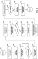
- FIG. 3 A method of operating the system 200 to process a substrate is illustrated in FIG. 3 .
- the system 200 starts with the isolation valves 212, 213 open.
- the substrate is inserted by a robot 106 or 108 through the open valves 212, 213 and the second chamber 204 into the first chamber 202 (at operation 302).
- the controller can operate the robot to carry the substrate 10 into the first chamber 202 and to place the substrate 10 on the pedestal.
- the vacuum system is used to further pump down the first chamber 202 to a second pressure that is lower than the first pressure, and to pump down the second chamber 204 to a third pressure that is lower than the second pressure (at operation 308).
- both the first and the second pressure can be 1-50 milliTorr.
- the first pressure can be 100-300 milliTorr and the second pressure can be 1-50 milliTorr.
- the substrate 10 is now processed in the first chamber 202 (at operation 324). Processing can proceed for a set time, e.g., as measured by a timer in the controller.
- the first gas can be an annealing gas that reacts with the layer on the substrate 10. Alternatively, the gas can include the material to be deposited onto the substrate 10.
- the proper temperature and pressure conditions in the first chamber 202 can cause the annealing or deposition of the material to occur.
- the controller can operate the one or more heating elements 219 in the support 218 to add heat to the substrate 10 to facilitate processing of the layer of material on the substrate 10.
- the outer isolation valve 216 is closed, and the inner isolation valve 230 is opened (at operation 326). This couples just the first chamber 202 to the exhaust system, while the second chamber 204 remains sealed.
- the inner chamber is pumped down to a sixth pressure (at operation 328).
- the sixth pressure can be less than the first pressure but greater than the third pressure, e.g., about equal to the second pressure.
- the pressure is at a near-vacuum pressure such that the pressure differential between the first chamber 202 and the second chamber 204 is small.
- the controller can compare the measured pressures (at operation 330). If the difference between the pressure P1 in the first chamber and the pressure P2 in the second chamber does not exceed the threshold value, then the evacuation of the chambers can be continued.
- the first isolation valve 212 is opened (at operation 232).
- the second isolation valve can be opened as well.
- the outer exhaust isolation valve 116 is opened. Because both inner and outer exhausts share the same foreline, keeping the outer exhaust isolation valve closed during inner exhausting can protect the lift pin and heater bellows from damage.
- the substrate 10 can be removed from the first chamber 202 using the robot 106 or 108, and, if necessary, transferred to a subsequent process chamber.
- FIG. 4 illustrates a controlled high-pressure processing system 200' that creates a high-pressure environment for processing a substrate and a low-pressure environment for the substrate when the substrate is being transferred between processing chambers.
- the system 200' can be the same as the system 200, except that the second gas delivery module 244' is a high pressure gas delivery module that can deliver a second gas to the first chamber 202 at high pressures, e.g., at pressures of 7500.6 - 60004.8 Torr (10 - 80 bar).
- the second gas is a liquid vapor, e.g., steam.
- the valve 234' in the delivery line 254 is a second high pressure isolation valve.
- FIG. 5 A method of operating the system 200 or 200' to process a substrate is illustrated in FIG. 5 . This process similar to the process described with reference to FIG. 3 , except as discussed below.
- the inner exhaust isolation valve 230 is closed (at operation 312'), and the high-pressure isolation valve 232 and/or 234' is opened (at operation 316').
- the first gas delivery module 242 and/or the second gas delivery module 244' delivers the first gas and/or the second gas to the first chamber 202 (at operation 318'). This raises the pressure in the first chamber 202 from the second pressure to the fifth pressure.
- the fifth pressure can be 7600 - 60800 Torr (10 - 80 atmospheres). Delivery of the gas by the first gas delivery module 244 can be controlled by the controller 210 using a pressure servo control algorithm.
- FIG. 4 illustrates a possible configuration for a first chamber 202 and second chamber 204 in a high-pressure processing system 200 (or 200').
- the high-pressure processing system 200 further includes the valve assembly 212 between the first chamber 202 and the second chamber 204.
- This implementation can have the second chamber 204 be part of the transfer chamber, e.g., be in pressure equilibrium.
- the second chamber 204 can be defined by volume between inner walls 420 and outer walls 424.
- the substrate 10 is supportable on a pedestal 418 (that provides the substrate support 218).
- One or more elements 219 e.g., a resistive heater, can be embedded in the pedestal 418.
- the substrate can sit directly on the pedestal 418, or sit on a lift pin assembly 430 that extends through the pedestal.
- the valve assembly 212 is formed by an arm 425 movable relative to the inner walls 420 and the base 422 of the first chamber 202.
- the valve assembly 212 includes a slit valve 423 between the first chamber 202 and the second chamber 204.
- the slit valve 423 includes a slit 423a and the arm 425.
- the slit 423a extends through one of the inner walls 420 of the first chamber 402.
- a vertical end 425a of the arm 425 is positioned outside of the first chamber 202 while a horizontal end 425b of the arm 425 is positioned within the first chamber 202.
- the vertical end 425a of the arm 425 can be positioned within the second chamber 204 and be driven by an actuator positioned within the second chamber 204.
- the vertical end 425a of the arm 425 is positioned outside of the second chamber 204 and is thus driven by an actuator 428 that is also positioned outside of the second chamber 204.
- the arm 425 extends through the slit 423a and is movable relative to the walls 420 so that the arm 425 can be moved to a position in which it forms a seal with the walls 420.
- the actuator 428 is coupled to the vertical end 425a of the arm 425 and drives the horizontal end 425b of the arm 425 relative to the walls 420.
- the arm 425 is movable vertically to cover or uncover the slit 423a.
- the vertical end 425a of the arm 425 can be or include a flange that extends substantially parallel to the adjacent inner surface of the inner wall 420.
- the arm 425 can also be driven laterally so that the horizontal end 425b of the arm 425 can engage or disengage the wall 420.
- the arm 425 can also extend through an aperture 426 in the outer wall 424.
- the valve assembly 212 is movable between an open position and a closed position.
- the horizontal end 425b of the arm 425 is spaced laterally apart from the wall 420, e.g., the inner surface of the wall 420.
- the horizontal end 425b of the arm 425 is positioned vertically so that the slit 423a is uncovered.
- the slit 423a thus provides an opening that enables fluidic communication between the first chamber 202 and the second chamber 204 and that also enables the substrate 10 to be moved in and out of the first chamber 202, e.g., by a robot as discussed above.
- the horizontal end 425b of the arm 425 covers the slit 423a and contacts one of the walls 420, thereby forming the seal to isolate the first chamber 202 from the second chamber 204.
- the flange or horizontal end 425b contacts an inner surface of the wall 420 defining the first chamber 202.
- An O-ring is placed along the circumference of the horizontal end 425b on the surface that contacts the wall 420, helping to reinforcing the seal of containment when the first chamber 402 is pressurized.
- the arm 425 can includes an internal gas channel 480.
- the internal gas channel 480 is supplied from cooling gas supply 484 and is a conduit to let the cooling gas flow through the arm 425.
- the internal gas channel 480 can extend through the horizontal end 425b, or through both the horizontal end 425b and the vertical end 425a.
- the internal gas channel and cooling gas supply 484 can be configured such that when the valve assembly 212 is in the open position no gas is available from the cooling gas supply 484, preventing cooling gas flow when transfer of the substrate is occurring.
- a metal silicide layer from a cobalt or nickel layer film
- other materials can include titanium, tantalum, tungsten, molybdenum, platinum, iron, niobium, palladium, and combinations thereof, and other alloys including nickel cobalt alloys, cobalt tungsten alloys, cobalt nickel tungsten alloys, doped cobalt and nickel alloys, or nickel iron alloys, to form the metal silicide material as described herein.
- the high-pressure chamber can be used for an etching system.
- the high-pressure chamber can be filled with an inert gas, and the high-pressure chamber can be used purely for heat treatment at high pressure.
- the processing platforms described herein can include other types of processing chambers.
- a processing platform can include an etching chamber to etch patterns onto a surface of a substrate.
- Each of the different chambers of a processing platform can have varying pressure environments, ranging from near-vacuum to more than 38000 Torr (50 atmospheres).
- the isolation valves, e.g., vacuum valves, between the chambers can isolate the pressures from one another such that these varying pressure environments can be maintained within each chamber.
Landscapes
- Chemical & Material Sciences (AREA)
- Metallurgy (AREA)
- Chemical Kinetics & Catalysis (AREA)
- Engineering & Computer Science (AREA)
- Materials Engineering (AREA)
- Mechanical Engineering (AREA)
- General Chemical & Material Sciences (AREA)
- Organic Chemistry (AREA)
- Container, Conveyance, Adherence, Positioning, Of Wafer (AREA)
- Chemical Vapour Deposition (AREA)
- Physical Vapour Deposition (AREA)
- Electrodes Of Semiconductors (AREA)
- Filling Or Discharging Of Gas Storage Vessels (AREA)
Claims (15)
- Hochdruckverarbeitungssystem zum Verarbeiten einer Schicht auf einem Substrat (10), das System umfassend:eine erste Kammer (202);eine Stütze (218) zum Halten des Substrats (10) in der ersten Kammer (202);eine zweite Kammer (204), die an die erste Kammer (202) angrenzt;eine Vorvakuumleitung (214) zum Entfernen von Gas aus der zweiten Kammer (204);Vakuumverarbeitungssystem (208), das so konfiguriert ist, dass es den Druck innerhalb der zweiten Kammer (204) auf nahezu Vakuum senkt;eine Ventilbaugruppe (212) zwischen der ersten Kammer und der zweiten Kammer zum Trennen des Drucks innerhalb der ersten Kammer (202) von dem Druck innerhalb der zweiten Kammer (204);ein Gaszufuhrsystem (206) das so konfiguriert ist, dass es ein oder mehrere Gase in die erste Kammer (202) einleitet und den Druck innerhalb der ersten Kammer (202) auf mindestens 7600 Torr (10 Atmosphären) erhöht, während sich das Gas in der ersten Kammer (202) befindet und während die erste Kammer (202) von der zweiten Kammer (204) getrennt ist, das Gaszufuhrsystem (206) aufweisend:ein erstes Gaszufuhrmodul (242) zum Zuführen eines ersten Gases bei einem ersten Druck, der mindestens 7600 Torr (10 Atmosphären) beträgt; undein zweites Gaszufuhrmodul (244) zum Zuführen des ersten Gases oder eines zweiten Gases mit einer unterschiedlichen Zusammensetzung bei einem zweiten Druck, der niedriger als der erste Druck, aber höher als 760 Torr (1 Atmosphäre) ist;eine Steuerung (210), die so konfiguriert ist, dass sie das Gaszufuhrsystem (206) und die Ventilbaugruppe (212) betreibt;ein erstes Abgassystem, umfassend eine Abgasleitung (211) zum Entfernen von Gas aus der ersten Kammer (202); undein gemeinsames Gehäuse (246), das sowohl das erste Gaszufuhrmodul (242) als auch das zweite Gaszufuhrmodul (244) umgibt; undein zweites Abgassystem, das so konfiguriert ist, dass es Gas aus dem gemeinsamen Gehäuse (246) entfernt.
- System nach Anspruch 1, wobei ein Innenraum des Gehäuses (246) von anderen Aufnahmebehältern des Hochdruckverarbeitungssystems fluidisch getrennt ist.
- System nach Anspruch 1, wobei das zweite Abgassystem so konfiguriert ist, dass es Gas aus dem Gehäuse (246) zu der Vorvakuumleitung (214) leitet.
- System nach Anspruch 1, umfassend eine erste und eine zweite Zuführungsleitung (252), (254), die das erste und zweite das Gaszufuhrmodul (242), (244) mit der ersten Kammer (202) verbinden, und ein Rückhaltegehäuse (260), das so konfiguriert ist, dass es Gas, das aus der ersten und der zweiten Zuführungsleitung (252), (254) entweicht, zu der Vorvakuumleitung (214) umleitet.
- System nach Anspruch 4, wobei das gemeinsame Gehäuse (246) von dem Rückhaltegehäuse (260) fluidisch getrennt ist.
- Hochdruckverarbeitungssystem nach Anspruch 1, wobei die Steuerung (210) so konfiguriert ist, dass sie das Vakuumverarbeitungssystem (208) und das erste Abgassystem so betreibt, dass die Ventilbaugruppe (212) die erste Kammer (202) von der zweiten Kammer (204) trennt, dann das zweite Gaszufuhrmodul (244) die erste Kammer (202) von einem Druck unter 760 Torr (1 Atmosphäre) auf den zweiten Druck anhebt, dann das zweite Gaszufuhrmodul (244) von der ersten Kammer getrennt wird und dann das erste Gaszufuhrmodul (242) die erste Kammer (202) von dem zweiten Druck auf den ersten Druck anhebt.
- System nach Anspruch 6, wobei das erste Gaszufuhrmodul (242) eine Pumpe umfasst, die so konfiguriert ist, dass sie den Druck des ersten Gases erhöht, bevor sie das erste Gas an die erste Kammer (202) zuführt.
- System nach Anspruch 7, wobei das zweite Gaszufuhrmodul (244) einen Massendurchflussregler, Flüssigkeitsdurchflussmesser oder Flüssigkeitsdurchflussregler, zum Leiten des Gases in die erste Kammer verwendet.
- System nach Anspruch 6, umfassend einen ersten Drucksensor (282) in der ersten Kammer und einen zweiten Drucksensor (282) in der zweiten Kammer.
- System nach Anspruch 9, wobei die Steuerung (210) so konfiguriert ist, dass sie das erste Abgassystem veranlasst, den Druck in der ersten Kammer (202) zu reduzieren, und das Vakuumverarbeitungssystem (208) veranlasst, den Druck in der zweiten Kammer (204) zu reduzieren, und wobei die Steuerung (210) so konfiguriert ist, dass sie Messungen von dem ersten Drucksensor (282) und dem zweiten Drucksensor (282) vergleicht und das erste Abgassystem und das Vakuumverarbeitungssystem (208) so steuert, dass ein Druck in der ersten Kammer (202) höher als ein Druck in der zweiten Kammer (204) ist.
- Verfahren zum Betreiben eines Hochdruckverarbeitungssystems, umfassend:Bringen einer ersten Kammer (202) und einer zweiten Kammer (204) auf einen ersten Druck, der weniger als 760 Torr (1 Atmosphäre) beträgt;während ein Trennventil (212) zwischen der ersten Kammer (202) und der zweiten Kammer (204) geöffnet ist, Transportieren eines Substrats (10) von der zweiten Kammer (204) in die erste Kammer (202);während das Trennventil (212) geschlossen ist, Reduzieren der ersten Kammer (202) von dem ersten Druck auf einen zweiten Druck und Reduzieren der zweiten Kammer (204) von dem ersten Druck auf einen dritten Druck;Unterdrucksetzen der ersten Kammer (202) auf einen vierten Druck, der über dem Atmosphärendruck und kleiner als 7600 Torr (10 Atmosphären) liegt, mit einem zweiten Gaszufuhrmodul (244);Unterdrucksetzen der ersten Kammer (202) auf einen fünften Druck, der über 7600 Torr (über 10 Atmosphären) liegt, mit einem ersten Gaszufuhrmodul (242);Verarbeiten des Substrats (10) während die erste Kammer (202) unter dem fünften Druck steht;Evakuieren der ersten Kammer (202); undÖffnen des Trennventils und Entfernen des Substrats (10) aus der ersten Kammer (202);wobei das erste Gaszufuhrmodul (242) und das zweite Gaszufuhrmodul (244) beide durch ein gemeinsames Gehäuse (246) umgeben sind, ein erstes Abgassystem eine Abgasleitung (211) zum Entfernen von Gas aus der ersten Kammer (202) umfasst, und ein zweites Abgassystem zum Entfernen von Gas aus dem gemeinsamen Gehäuse (246) konfiguriert ist.
- Verfahren nach Anspruch 11, wobei das Unterdrucksetzen der ersten Kammer (202) auf den fünften Druck das Zuführen eines ersten Gases zu der ersten Kammer (202) umfasst, und das Unterdrucksetzen der ersten Kammer (202) auf den vierten Druck das Zuführen eines zweiten Gases mit einer anderen Zusammensetzung zu der ersten Kammer (202) umfasst.
- Verfahren nach Anspruch 11, wobei das erste Gas mindestens eines von H2 oder NH3 aufweist.
- Verfahren nach Anspruch 11, wobei das Unterdrucksetzen der ersten Kammer (202) mit dem zweiten Gaszufuhrmodul das Trennen des ersten Gaszufuhrmoduls (242) von der ersten Kammer (202) mit einem Hochdrucktrennventil (232) in einer Zufuhrleitung zwischen dem ersten Gaszufuhrmodul (242) und der ersten Kammer (202) und das fluidische Koppeln des zweiten Gaszufuhrmoduls (244) und der ersten Kammer (202) durch Öffnen eines Niederdrucktrennventils (234) in einer Zufuhrleitung zwischen dem zweiten Gaszufuhrmodul (244) und der ersten Kammer (242) umfasst.
- Verfahren nach Anspruch 14, wobei das Unterdrucksetzen der ersten Kammer (202) mit dem ersten Gaszufuhrmodul (242) das Trennen des zweiten Gaszufuhrmoduls (244) von der ersten Kammer (202) mit dem Niederdrucktrennventil (234) und das fluidische Koppeln des ersten Gaszufuhrmoduls (242) und der ersten Kammer (202) durch Öffnen des Hochdrucktrennventils (232) umfasst.
Priority Applications (1)
| Application Number | Priority Date | Filing Date | Title |
|---|---|---|---|
| EP23219233.6A EP4321649B1 (de) | 2017-11-11 | 2018-11-07 | Gaszufuhrsystem für hochdruckverarbeitungskammer |
Applications Claiming Priority (2)
| Application Number | Priority Date | Filing Date | Title |
|---|---|---|---|
| US201762584794P | 2017-11-11 | 2017-11-11 | |
| PCT/US2018/059643 WO2019094481A1 (en) | 2017-11-11 | 2018-11-07 | Gas delivery system for high pressure processing chamber |
Related Child Applications (1)
| Application Number | Title | Priority Date | Filing Date |
|---|---|---|---|
| EP23219233.6A Division EP4321649B1 (de) | 2017-11-11 | 2018-11-07 | Gaszufuhrsystem für hochdruckverarbeitungskammer |
Publications (3)
| Publication Number | Publication Date |
|---|---|
| EP3707746A1 EP3707746A1 (de) | 2020-09-16 |
| EP3707746A4 EP3707746A4 (de) | 2021-08-18 |
| EP3707746B1 true EP3707746B1 (de) | 2023-12-27 |
Family
ID=66432396
Family Applications (2)
| Application Number | Title | Priority Date | Filing Date |
|---|---|---|---|
| EP18876650.5A Active EP3707746B1 (de) | 2017-11-11 | 2018-11-07 | Gaszufuhrsystem für hochdruckprozesskammer |
| EP23219233.6A Active EP4321649B1 (de) | 2017-11-11 | 2018-11-07 | Gaszufuhrsystem für hochdruckverarbeitungskammer |
Family Applications After (1)
| Application Number | Title | Priority Date | Filing Date |
|---|---|---|---|
| EP23219233.6A Active EP4321649B1 (de) | 2017-11-11 | 2018-11-07 | Gaszufuhrsystem für hochdruckverarbeitungskammer |
Country Status (8)
| Country | Link |
|---|---|
| US (3) | US10720341B2 (de) |
| EP (2) | EP3707746B1 (de) |
| JP (2) | JP7112490B2 (de) |
| KR (3) | KR102585074B1 (de) |
| CN (3) | CN117936417A (de) |
| SG (1) | SG11202003355QA (de) |
| TW (2) | TWI849834B (de) |
| WO (1) | WO2019094481A1 (de) |
Families Citing this family (39)
| Publication number | Priority date | Publication date | Assignee | Title |
|---|---|---|---|---|
| US10224224B2 (en) * | 2017-03-10 | 2019-03-05 | Micromaterials, LLC | High pressure wafer processing systems and related methods |
| US10622214B2 (en) | 2017-05-25 | 2020-04-14 | Applied Materials, Inc. | Tungsten defluorination by high pressure treatment |
| KR102405723B1 (ko) | 2017-08-18 | 2022-06-07 | 어플라이드 머티어리얼스, 인코포레이티드 | 고압 및 고온 어닐링 챔버 |
| US10276411B2 (en) | 2017-08-18 | 2019-04-30 | Applied Materials, Inc. | High pressure and high temperature anneal chamber |
| WO2019055415A1 (en) | 2017-09-12 | 2019-03-21 | Applied Materials, Inc. | APPARATUS AND METHODS FOR MANUFACTURING SEMICONDUCTOR STRUCTURES USING A PROTECTIVE BARRIER LAYER |
| EP3707746B1 (de) | 2017-11-11 | 2023-12-27 | Micromaterials LLC | Gaszufuhrsystem für hochdruckprozesskammer |
| WO2019099125A1 (en) | 2017-11-16 | 2019-05-23 | Applied Materials, Inc. | High pressure steam anneal processing apparatus |
| JP2021503714A (ja) | 2017-11-17 | 2021-02-12 | アプライド マテリアルズ インコーポレイテッドApplied Materials,Incorporated | 高圧処理システムのためのコンデンサシステム |
| KR102702244B1 (ko) | 2018-03-09 | 2024-09-03 | 어플라이드 머티어리얼스, 인코포레이티드 | 금속 함유 재료들을 위한 고압 어닐링 프로세스 |
| KR20250174989A (ko) * | 2018-03-27 | 2025-12-15 | 아즈테라피즈 인코포레이티드 | 신경변성 질환을 치료하기 위한 CAR-Treg-기반 요법 |
| US10714331B2 (en) | 2018-04-04 | 2020-07-14 | Applied Materials, Inc. | Method to fabricate thermally stable low K-FinFET spacer |
| US10950429B2 (en) | 2018-05-08 | 2021-03-16 | Applied Materials, Inc. | Methods of forming amorphous carbon hard mask layers and hard mask layers formed therefrom |
| US10748783B2 (en) | 2018-07-25 | 2020-08-18 | Applied Materials, Inc. | Gas delivery module |
| US10675581B2 (en) | 2018-08-06 | 2020-06-09 | Applied Materials, Inc. | Gas abatement apparatus |
| DE102018120580A1 (de) * | 2018-08-23 | 2020-02-27 | Infineon Technologies Ag | Vorrichtung und verfahren zum abscheiden einer schicht bei atmosphärendruck |
| US11380564B2 (en) | 2018-09-19 | 2022-07-05 | Applied Materials, Inc. | Processing system having a front opening unified pod (FOUP) load lock |
| JP7179172B6 (ja) | 2018-10-30 | 2022-12-16 | アプライド マテリアルズ インコーポレイテッド | 半導体用途の構造体をエッチングするための方法 |
| CN112996950B (zh) | 2018-11-16 | 2024-04-05 | 应用材料公司 | 使用增强扩散工艺的膜沉积 |
| WO2020117462A1 (en) | 2018-12-07 | 2020-06-11 | Applied Materials, Inc. | Semiconductor processing system |
| US11901222B2 (en) | 2020-02-17 | 2024-02-13 | Applied Materials, Inc. | Multi-step process for flowable gap-fill film |
| KR102885309B1 (ko) | 2020-08-26 | 2025-11-13 | 주식회사 원익아이피에스 | 기판처리방법과, 그에 따른 기판처리장치 및 반도체 소자 제조방법 |
| KR102816044B1 (ko) | 2020-10-28 | 2025-06-04 | 주식회사 원익아이피에스 | 기판 처리 방법 |
| TW202229620A (zh) * | 2020-11-12 | 2022-08-01 | 特文特大學 | 沉積系統、用於控制反應條件之方法、沉積方法 |
| KR102852007B1 (ko) * | 2020-12-30 | 2025-08-29 | 세메스 주식회사 | 지지 장치 및 지지 장치를 포함하는 기판 처리 장치 |
| US12191214B2 (en) * | 2021-03-05 | 2025-01-07 | Taiwan Semiconductor Manufacturing Company Limited | System and methods for controlling an amount of primer in a primer application gas |
| FI129948B (en) * | 2021-05-10 | 2022-11-15 | Picosun Oy | SUBSTRATE PROCESSING EQUIPMENT AND METHOD |
| FI130021B (en) | 2021-05-10 | 2022-12-30 | Picosun Oy | Substrate processing apparatus and method |
| FI130020B (en) * | 2021-05-10 | 2022-12-30 | Picosun Oy | Substrate processing apparatus and method |
| JP2024526539A (ja) * | 2021-06-14 | 2024-07-19 | ラム リサーチ コーポレーション | 基板の移動を防止するための前面圧力および裏面圧力の監視 |
| US20230060192A1 (en) * | 2021-09-02 | 2023-03-02 | Entegris, Inc. | Methods and apparatus for processing an electrostatic chuck |
| JP7726746B2 (ja) * | 2021-11-09 | 2025-08-20 | 東京エレクトロン株式会社 | 基板処理システム |
| CN114256104B (zh) * | 2021-11-29 | 2026-01-30 | 西安北方华创微电子装备有限公司 | 腔室泄漏检测方法和半导体工艺设备 |
| KR102396669B1 (ko) * | 2021-12-20 | 2022-05-12 | 주식회사 에이치피에스피 | 반도체 챔버의 공정 전과 공정 후 잔류 가스 검출 장치 |
| KR102452714B1 (ko) * | 2021-12-23 | 2022-10-07 | 주식회사 에이치피에스피 | 고압 및 진공공정 병행 챔버장치 |
| JP2023173097A (ja) * | 2022-05-25 | 2023-12-07 | 東京エレクトロン株式会社 | 基板処理装置及び酸素混入抑制方法 |
| KR20240028609A (ko) * | 2022-08-25 | 2024-03-05 | 주식회사 원익아이피에스 | 기판처리장치 및 가스공급방법 |
| US12442074B2 (en) * | 2022-08-25 | 2025-10-14 | Applied Materials, Inc. | System and method for controlling foreline pressure |
| KR102614456B1 (ko) * | 2023-05-22 | 2023-12-19 | 주식회사 에이치피에스피 | 고압 기판 처리 장치 |
| KR102784932B1 (ko) | 2024-04-09 | 2025-03-25 | 주식회사 에이치피에스피 | 기판 처리 장치 |
Family Cites Families (610)
| Publication number | Priority date | Publication date | Assignee | Title |
|---|---|---|---|---|
| US6482262B1 (en) | 1959-10-10 | 2002-11-19 | Asm Microchemistry Oy | Deposition of transition metal carbides |
| US4524587A (en) | 1967-01-10 | 1985-06-25 | Kantor Frederick W | Rotary thermodynamic apparatus and method |
| US3684592A (en) | 1969-09-30 | 1972-08-15 | Westinghouse Electric Corp | Passivated surfaces and protective coatings for semiconductor devices and processes for producing the same |
| US3758316A (en) | 1971-03-30 | 1973-09-11 | Du Pont | Refractory materials and process for making same |
| US3749383A (en) | 1971-04-29 | 1973-07-31 | Rca Corp | Apparatus for processing semiconductor devices |
| US4409260A (en) | 1979-08-15 | 1983-10-11 | Hughes Aircraft Company | Process for low-temperature surface layer oxidation of a semiconductor substrate |
| US4424101A (en) | 1980-11-06 | 1984-01-03 | The Perkin-Elmer Corp. | Method of depositing doped refractory metal silicides using DC magnetron/RF diode mode co-sputtering techniques |
| GB2106709B (en) * | 1981-09-17 | 1986-11-12 | Itt Ind Ltd | Semiconductor processing |
| US4589193A (en) | 1984-06-29 | 1986-05-20 | International Business Machines Corporation | Metal silicide channel stoppers for integrated circuits and method for making the same |
| US4576652A (en) | 1984-07-12 | 1986-03-18 | International Business Machines Corporation | Incoherent light annealing of gallium arsenide substrate |
| JPS634616A (ja) | 1986-06-25 | 1988-01-09 | Hitachi Tokyo Electron Co Ltd | 蒸気処理装置 |
| JPS6367721A (ja) | 1986-09-09 | 1988-03-26 | Meidensha Electric Mfg Co Ltd | アモルフアス炭素半導体膜の製造方法 |
| JPH0748489B2 (ja) * | 1987-07-27 | 1995-05-24 | 富士通株式会社 | プラズマ処理装置 |
| US4879259A (en) | 1987-09-28 | 1989-11-07 | The Board Of Trustees Of The Leland Stanford Junion University | Rapid thermal annealing of gallium arsenide with trimethyl arsenic overpressure |
| CA1308496C (en) | 1988-02-18 | 1992-10-06 | Rajiv V. Joshi | Deposition of tungsten on silicon in a non-self-limiting cvd process |
| US5114513A (en) | 1988-10-27 | 1992-05-19 | Omron Tateisi Electronics Co. | Optical device and manufacturing method thereof |
| US5167717A (en) | 1989-02-15 | 1992-12-01 | Charles Boitnott | Apparatus and method for processing a semiconductor wafer |
| JP2730695B2 (ja) | 1989-04-10 | 1998-03-25 | 忠弘 大見 | タングステン膜の成膜装置 |
| US5126117A (en) | 1990-05-22 | 1992-06-30 | Custom Engineered Materials, Inc. | Device for preventing accidental releases of hazardous gases |
| US5175123A (en) | 1990-11-13 | 1992-12-29 | Motorola, Inc. | High-pressure polysilicon encapsulated localized oxidation of silicon |
| US5050540A (en) | 1991-01-29 | 1991-09-24 | Arne Lindberg | Method of gas blanketing a boiler |
| JP2996524B2 (ja) | 1991-03-18 | 2000-01-11 | 松下電子工業株式会社 | ポリイミド硬化装置 |
| US5314541A (en) | 1991-05-28 | 1994-05-24 | Tokyo Electron Limited | Reduced pressure processing system and reduced pressure processing method |
| DE69233222T2 (de) | 1991-05-28 | 2004-08-26 | Trikon Technologies Ltd., Thornbury | Verfahren zum Füllen eines Hohlraumes in einem Substrat |
| US6238588B1 (en) | 1991-06-27 | 2001-05-29 | Applied Materials, Inc. | High pressure high non-reactive diluent gas content high plasma ion density plasma oxide etch process |
| JPH0521310A (ja) | 1991-07-11 | 1993-01-29 | Canon Inc | 微細パタン形成方法 |
| JPH0521347A (ja) | 1991-07-11 | 1993-01-29 | Canon Inc | スパツタリング装置 |
| JPH05129296A (ja) | 1991-11-05 | 1993-05-25 | Fujitsu Ltd | 導電膜の平坦化方法 |
| US5300320A (en) | 1992-06-23 | 1994-04-05 | President And Fellows Of Harvard College | Chemical vapor deposition from single organometallic precursors |
| US5319212A (en) | 1992-10-07 | 1994-06-07 | Genus, Inc. | Method of monitoring ion beam current in ion implantation apparatus for use in manufacturing semiconductors |
| JPH06283496A (ja) | 1993-03-26 | 1994-10-07 | Dainippon Screen Mfg Co Ltd | 洗浄処理後の基板の乾燥処理装置 |
| US5607002A (en) | 1993-04-28 | 1997-03-04 | Advanced Delivery & Chemical Systems, Inc. | Chemical refill system for high purity chemicals |
| US5578132A (en) | 1993-07-07 | 1996-11-26 | Tokyo Electron Kabushiki Kaisha | Apparatus for heat treating semiconductors at normal pressure and low pressure |
| JPH0766424A (ja) | 1993-08-20 | 1995-03-10 | Semiconductor Energy Lab Co Ltd | 半導体装置およびその作製方法 |
| JPH07158767A (ja) | 1993-12-09 | 1995-06-20 | Kokusai Electric Co Ltd | ゲートバルブ |
| US5460689A (en) | 1994-02-28 | 1995-10-24 | Applied Materials, Inc. | High pressure plasma treatment method and apparatus |
| US5880041A (en) | 1994-05-27 | 1999-03-09 | Motorola Inc. | Method for forming a dielectric layer using high pressure |
| US5597439A (en) | 1994-10-26 | 1997-01-28 | Applied Materials, Inc. | Process gas inlet and distribution passages |
| US5808245A (en) | 1995-01-03 | 1998-09-15 | Donaldson Company, Inc. | Vertical mount catalytic converter muffler |
| JPH08195493A (ja) | 1995-01-13 | 1996-07-30 | Toshiba Corp | 薄膜トランジスタの製造方法 |
| US5620524A (en) | 1995-02-27 | 1997-04-15 | Fan; Chiko | Apparatus for fluid delivery in chemical vapor deposition systems |
| US5858051A (en) | 1995-05-08 | 1999-01-12 | Toshiba Machine Co., Ltd. | Method of manufacturing optical waveguide |
| JP2872637B2 (ja) | 1995-07-10 | 1999-03-17 | アプライド マテリアルズ インコーポレイテッド | マイクロ波プラズマベースアプリケータ |
| JP3684624B2 (ja) | 1995-08-02 | 2005-08-17 | ソニー株式会社 | 反応ガス供給装置 |
| US5747383A (en) | 1995-09-05 | 1998-05-05 | Taiwan Semiconductor Manufacturing Company Ltd | Method for forming conductive lines and stacked vias |
| US5857368A (en) | 1995-10-06 | 1999-01-12 | Applied Materials, Inc. | Apparatus and method for fabricating metal paths in semiconductor substrates through high pressure extrusion |
| JPH09296267A (ja) * | 1995-11-21 | 1997-11-18 | Applied Materials Inc | 高圧押出しによる、半導体基板における金属パスの製造装置および方法 |
| US5877087A (en) | 1995-11-21 | 1999-03-02 | Applied Materials, Inc. | Low temperature integrated metallization process and apparatus |
| US5677230A (en) | 1995-12-01 | 1997-10-14 | Motorola | Method of making wide bandgap semiconductor devices |
| US6077571A (en) | 1995-12-19 | 2000-06-20 | The Research Foundation Of State University Of New York | Conformal pure and doped aluminum coatings and a methodology and apparatus for their preparation |
| US5895274A (en) | 1996-01-22 | 1999-04-20 | Micron Technology, Inc. | High-pressure anneal process for integrated circuits |
| US5918149A (en) | 1996-02-16 | 1999-06-29 | Advanced Micro Devices, Inc. | Deposition of a conductor in a via hole or trench |
| KR980012044A (ko) | 1996-03-01 | 1998-04-30 | 히가시 데츠로 | 기판건조장치 및 기판건조방법 |
| US5998305A (en) | 1996-03-29 | 1999-12-07 | Praxair Technology, Inc. | Removal of carbon from substrate surfaces |
| US5738915A (en) | 1996-09-19 | 1998-04-14 | Lambda Technologies, Inc. | Curing polymer layers on semiconductor substrates using variable frequency microwave energy |
| US6444037B1 (en) | 1996-11-13 | 2002-09-03 | Applied Materials, Inc. | Chamber liner for high temperature processing chamber |
| US6082950A (en) | 1996-11-18 | 2000-07-04 | Applied Materials, Inc. | Front end wafer staging with wafer cassette turntables and on-the-fly wafer center finding |
| US5886864A (en) | 1996-12-02 | 1999-03-23 | Applied Materials, Inc. | Substrate support member for uniform heating of a substrate |
| TW347570B (en) | 1996-12-24 | 1998-12-11 | Toshiba Co Ltd | Semiconductor device and method for manufacturing the same |
| US5888888A (en) | 1997-01-29 | 1999-03-30 | Ultratech Stepper, Inc. | Method for forming a silicide region on a silicon body |
| JP2980052B2 (ja) | 1997-03-31 | 1999-11-22 | 日本電気株式会社 | 半導体装置の製造方法 |
| US6334249B2 (en) | 1997-04-22 | 2002-01-01 | Texas Instruments Incorporated | Cavity-filling method for reducing surface topography and roughness |
| KR100560049B1 (ko) | 1997-05-10 | 2006-05-25 | 가부시키가이샤 한도오따이 에네루기 켄큐쇼 | 성막방법 |
| JP2976931B2 (ja) | 1997-06-04 | 1999-11-10 | 日本電気株式会社 | 半導体装置の製造方法 |
| US6309713B1 (en) | 1997-06-30 | 2001-10-30 | Applied Materials, Inc. | Deposition of tungsten nitride by plasma enhanced chemical vapor deposition |
| US6136664A (en) | 1997-08-07 | 2000-10-24 | International Business Machines Corporation | Filling of high aspect ratio trench isolation |
| US20030049372A1 (en) | 1997-08-11 | 2003-03-13 | Cook Robert C. | High rate deposition at low pressures in a small batch reactor |
| KR100261017B1 (ko) | 1997-08-19 | 2000-08-01 | 윤종용 | 반도체 장치의 금속 배선층을 형성하는 방법 |
| US6348376B2 (en) | 1997-09-29 | 2002-02-19 | Samsung Electronics Co., Ltd. | Method of forming metal nitride film by chemical vapor deposition and method of forming metal contact and capacitor of semiconductor device using the same |
| US5963817A (en) | 1997-10-16 | 1999-10-05 | International Business Machines Corporation | Bulk and strained silicon on insulator using local selective oxidation |
| JP3199006B2 (ja) | 1997-11-18 | 2001-08-13 | 日本電気株式会社 | 層間絶縁膜の形成方法および絶縁膜形成装置 |
| US6442980B2 (en) | 1997-11-26 | 2002-09-03 | Chart Inc. | Carbon dioxide dry cleaning system |
| US6140235A (en) | 1997-12-05 | 2000-10-31 | Applied Materials, Inc. | High pressure copper fill at low temperature |
| KR100275727B1 (ko) | 1998-01-06 | 2001-01-15 | 윤종용 | 반도체 장치의 커패시터 형성방법 |
| JP3296281B2 (ja) | 1998-01-22 | 2002-06-24 | 日本電気株式会社 | スパッタリング装置及びスパッタリング方法 |
| US6846739B1 (en) | 1998-02-27 | 2005-01-25 | Micron Technology, Inc. | MOCVD process using ozone as a reactant to deposit a metal oxide barrier layer |
| US6164412A (en) | 1998-04-03 | 2000-12-26 | Arvin Industries, Inc. | Muffler |
| JP3955386B2 (ja) | 1998-04-09 | 2007-08-08 | 富士通株式会社 | 半導体装置及びその製造方法 |
| JPH11354515A (ja) | 1998-06-04 | 1999-12-24 | Ishikawajima Harima Heavy Ind Co Ltd | 加圧式加熱炉 |
| US6103585A (en) | 1998-06-09 | 2000-08-15 | Siemens Aktiengesellschaft | Method of forming deep trench capacitors |
| KR100319888B1 (ko) | 1998-06-16 | 2002-01-10 | 윤종용 | 선택적 금속층 형성방법, 이를 이용한 커패시터 형성 및 콘택홀 매립방법 |
| KR100287180B1 (ko) | 1998-09-17 | 2001-04-16 | 윤종용 | 계면 조절층을 이용하여 금속 배선층을 형성하는 반도체 소자의 제조 방법 |
| US6719516B2 (en) | 1998-09-28 | 2004-04-13 | Applied Materials, Inc. | Single wafer load lock with internal wafer transport |
| KR100327328B1 (ko) | 1998-10-13 | 2002-05-09 | 윤종용 | 부분적으로다른두께를갖는커패시터의유전막형성방버뵤 |
| US20030101938A1 (en) | 1998-10-27 | 2003-06-05 | Applied Materials, Inc. | Apparatus for the deposition of high dielectric constant films |
| KR100331544B1 (ko) | 1999-01-18 | 2002-04-06 | 윤종용 | 반응챔버에 가스를 유입하는 방법 및 이에 사용되는 샤워헤드 |
| JP2000221799A (ja) | 1999-01-29 | 2000-08-11 | Canon Inc | 画像形成装置 |
| KR100804853B1 (ko) * | 1999-03-04 | 2008-02-20 | 서페이스 테크놀로지 시스템스 피엘씨 | 삼불화염소가스발생기시스템 |
| US6200893B1 (en) | 1999-03-11 | 2001-03-13 | Genus, Inc | Radical-assisted sequential CVD |
| US6305314B1 (en) | 1999-03-11 | 2001-10-23 | Genvs, Inc. | Apparatus and concept for minimizing parasitic chemical vapor deposition during atomic layer deposition |
| JP4096440B2 (ja) | 1999-03-11 | 2008-06-04 | 三菱瓦斯化学株式会社 | 多層成形品 |
| JP2002541664A (ja) | 1999-04-02 | 2002-12-03 | シリコン ヴァレイ グループ サーマル システムズ リミテッド ライアビリティ カンパニー | 側壁ライナー酸化成長前にトレンチ充填酸化物を付着させるためのトレンチ分離方法。 |
| JP3892621B2 (ja) | 1999-04-19 | 2007-03-14 | 株式会社神戸製鋼所 | 配線膜の形成方法 |
| US6086730A (en) | 1999-04-22 | 2000-07-11 | Komag, Incorporated | Method of sputtering a carbon protective film on a magnetic disk with high sp3 content |
| JP2000340671A (ja) | 1999-05-26 | 2000-12-08 | Fujitsu Ltd | 半導体装置の製造方法及び半導体装置 |
| JP2001053066A (ja) | 1999-05-28 | 2001-02-23 | Tokyo Electron Ltd | オゾン処理装置およびその方法 |
| US6355558B1 (en) | 1999-06-10 | 2002-03-12 | Texas Instruments Incorporated | Metallization structure, and associated method, to improve crystallographic texture and cavity fill for CVD aluminum/PVD aluminum alloy films |
| JP2000357699A (ja) | 1999-06-16 | 2000-12-26 | Seiko Epson Corp | 半導体装置 |
| EP1069213A3 (de) | 1999-07-12 | 2004-01-28 | Applied Materials, Inc. | Optimale Wärmebehandlungstechnik zur Steuerung von Mikrohohlräumenbildung und zur Selbst-Wärmebehandlungsverwaltung von Elektroplattiertem Kupfer |
| US6468490B1 (en) | 2000-06-29 | 2002-10-22 | Applied Materials, Inc. | Abatement of fluorine gas from effluent |
| US6612317B2 (en) | 2000-04-18 | 2003-09-02 | S.C. Fluids, Inc | Supercritical fluid delivery and recovery system for semiconductor wafer processing |
| US6334266B1 (en) | 1999-09-20 | 2002-01-01 | S.C. Fluids, Inc. | Supercritical fluid drying system and method of use |
| DE69940114D1 (de) | 1999-08-17 | 2009-01-29 | Applied Materials Inc | Oberflächenbehandlung von kohlenstoffdotierten SiO2-Filmen zur Erhöhung der Stabilität während der O2-Veraschung |
| US6299753B1 (en) | 1999-09-01 | 2001-10-09 | Applied Materials, Inc. | Double pressure vessel chemical dispenser unit |
| US6511539B1 (en) | 1999-09-08 | 2003-01-28 | Asm America, Inc. | Apparatus and method for growth of a thin film |
| JP2001110729A (ja) | 1999-10-06 | 2001-04-20 | Mitsubishi Heavy Ind Ltd | 半導体素子の連続製造装置 |
| FI117942B (fi) | 1999-10-14 | 2007-04-30 | Asm Int | Menetelmä oksidiohutkalvojen kasvattamiseksi |
| KR100304714B1 (ko) | 1999-10-20 | 2001-11-02 | 윤종용 | 금속 할로겐 가스를 사용한 반도체 소자의 금속 박막 형성방법 |
| US6444372B1 (en) | 1999-10-25 | 2002-09-03 | Svg Lithography Systems, Inc. | Non absorbing reticle and method of making same |
| US20030148631A1 (en) | 1999-11-08 | 2003-08-07 | Taiwan Semiconductor Manufacturing Company | Oxidative annealing method for forming etched spin-on-glass (SOG) planarizing layer with uniform etch profile |
| US6500603B1 (en) | 1999-11-11 | 2002-12-31 | Mitsui Chemicals, Inc. | Method for manufacturing polymer optical waveguide |
| KR100629255B1 (ko) | 1999-11-12 | 2006-09-29 | 삼성전자주식회사 | 반도체 포토 공정용 베이크 장치 |
| KR100321561B1 (ko) | 1999-11-16 | 2002-01-23 | 박호군 | 휘발 성분이 포함된 다성분 산화물 강유전체 박막의 제조방법 |
| US6399486B1 (en) | 1999-11-22 | 2002-06-04 | Taiwan Semiconductor Manufacturing Company | Method of improved copper gap fill |
| TW484170B (en) | 1999-11-30 | 2002-04-21 | Applied Materials Inc | Integrated modular processing platform |
| US6344419B1 (en) | 1999-12-03 | 2002-02-05 | Applied Materials, Inc. | Pulsed-mode RF bias for sidewall coverage improvement |
| US6969448B1 (en) | 1999-12-30 | 2005-11-29 | Cypress Semiconductor Corp. | Method for forming a metallization structure in an integrated circuit |
| US6150286A (en) | 2000-01-03 | 2000-11-21 | Advanced Micro Devices, Inc. | Method of making an ultra thin silicon nitride film |
| FI20000099A0 (fi) | 2000-01-18 | 2000-01-18 | Asm Microchemistry Ltd | Menetelmä metalliohutkalvojen kasvattamiseksi |
| US6541367B1 (en) | 2000-01-18 | 2003-04-01 | Applied Materials, Inc. | Very low dielectric constant plasma-enhanced CVD films |
| US6277249B1 (en) | 2000-01-21 | 2001-08-21 | Applied Materials Inc. | Integrated process for copper via filling using a magnetron and target producing highly energetic ions |
| US6251242B1 (en) | 2000-01-21 | 2001-06-26 | Applied Materials, Inc. | Magnetron and target producing an extended plasma region in a sputter reactor |
| US6319766B1 (en) | 2000-02-22 | 2001-11-20 | Applied Materials, Inc. | Method of tantalum nitride deposition by tantalum oxide densification |
| JP2001250787A (ja) | 2000-03-06 | 2001-09-14 | Hitachi Kokusai Electric Inc | 基板処理装置および基板処理方法 |
| AU2001245388A1 (en) | 2000-03-07 | 2001-09-17 | Asm America, Inc. | Graded thin films |
| US6475902B1 (en) * | 2000-03-10 | 2002-11-05 | Applied Materials, Inc. | Chemical vapor deposition of niobium barriers for copper metallization |
| US6506653B1 (en) | 2000-03-13 | 2003-01-14 | International Business Machines Corporation | Method using disposable and permanent films for diffusion and implant doping |
| JP4637989B2 (ja) | 2000-03-24 | 2011-02-23 | 株式会社神戸製鋼所 | 半導体配線膜の形成方法 |
| FI117979B (fi) | 2000-04-14 | 2007-05-15 | Asm Int | Menetelmä oksidiohutkalvojen valmistamiseksi |
| US20040025908A1 (en) | 2000-04-18 | 2004-02-12 | Stephen Douglas | Supercritical fluid delivery system for semiconductor wafer processing |
| KR100363088B1 (ko) | 2000-04-20 | 2002-12-02 | 삼성전자 주식회사 | 원자층 증착방법을 이용한 장벽 금속막의 제조방법 |
| US6482733B2 (en) | 2000-05-15 | 2002-11-19 | Asm Microchemistry Oy | Protective layers prior to alternating layer deposition |
| TW508658B (en) | 2000-05-15 | 2002-11-01 | Asm Microchemistry Oy | Process for producing integrated circuits |
| US6921722B2 (en) | 2000-05-30 | 2005-07-26 | Ebara Corporation | Coating, modification and etching of substrate surface with particle beam irradiation of the same |
| US6620723B1 (en) | 2000-06-27 | 2003-09-16 | Applied Materials, Inc. | Formation of boride barrier layers using chemisorption techniques |
| US7964505B2 (en) | 2005-01-19 | 2011-06-21 | Applied Materials, Inc. | Atomic layer deposition of tungsten materials |
| US6551929B1 (en) | 2000-06-28 | 2003-04-22 | Applied Materials, Inc. | Bifurcated deposition process for depositing refractory metal layers employing atomic layer deposition and chemical vapor deposition techniques |
| US6585823B1 (en) | 2000-07-07 | 2003-07-01 | Asm International, N.V. | Atomic layer deposition |
| US6491978B1 (en) * | 2000-07-10 | 2002-12-10 | Applied Materials, Inc. | Deposition of CVD layers for copper metallization using novel metal organic chemical vapor deposition (MOCVD) precursors |
| US7166524B2 (en) | 2000-08-11 | 2007-01-23 | Applied Materials, Inc. | Method for ion implanting insulator material to reduce dielectric constant |
| US6660660B2 (en) | 2000-10-10 | 2003-12-09 | Asm International, Nv. | Methods for making a dielectric stack in an integrated circuit |
| US6416822B1 (en) | 2000-12-06 | 2002-07-09 | Angstrom Systems, Inc. | Continuous method for depositing a film by modulated ion-induced atomic layer deposition (MII-ALD) |
| US6428859B1 (en) | 2000-12-06 | 2002-08-06 | Angstron Systems, Inc. | Sequential method for depositing a film by modulated ion-induced atomic layer deposition (MII-ALD) |
| KR100385947B1 (ko) | 2000-12-06 | 2003-06-02 | 삼성전자주식회사 | 원자층 증착 방법에 의한 박막 형성 방법 |
| US6630201B2 (en) | 2001-04-05 | 2003-10-07 | Angstron Systems, Inc. | Adsorption process for atomic layer deposition |
| US6464779B1 (en) | 2001-01-19 | 2002-10-15 | Novellus Systems, Inc. | Copper atomic layer chemical vapor desposition |
| US6852167B2 (en) | 2001-03-01 | 2005-02-08 | Micron Technology, Inc. | Methods, systems, and apparatus for uniform chemical-vapor depositions |
| JP4335469B2 (ja) * | 2001-03-22 | 2009-09-30 | 株式会社荏原製作所 | 真空排気装置のガス循環量調整方法及び装置 |
| US6797336B2 (en) * | 2001-03-22 | 2004-09-28 | Ambp Tech Corporation | Multi-component substances and processes for preparation thereof |
| TW544797B (en) | 2001-04-17 | 2003-08-01 | Kobe Steel Ltd | High-pressure processing apparatus |
| JP2002319571A (ja) | 2001-04-20 | 2002-10-31 | Kawasaki Microelectronics Kk | エッチング槽の前処理方法及び半導体装置の製造方法 |
| US7080651B2 (en) | 2001-05-17 | 2006-07-25 | Dainippon Screen Mfg. Co., Ltd. | High pressure processing apparatus and method |
| KR100433846B1 (ko) | 2001-05-23 | 2004-06-04 | 주식회사 하이닉스반도체 | 반도체장치의 금속도전막 형성방법 |
| US6752585B2 (en) | 2001-06-13 | 2004-06-22 | Applied Materials Inc | Method and apparatus for transferring a semiconductor substrate |
| EP1271636A1 (de) | 2001-06-22 | 2003-01-02 | Infineon Technologies AG | Steuerung eines thermischen Oxidationsprozesses durch Kontrolle des Partialdrucks des Oxidationsmittels |
| US20080268635A1 (en) | 2001-07-25 | 2008-10-30 | Sang-Ho Yu | Process for forming cobalt and cobalt silicide materials in copper contact applications |
| US20030029715A1 (en) | 2001-07-25 | 2003-02-13 | Applied Materials, Inc. | An Apparatus For Annealing Substrates In Physical Vapor Deposition Systems |
| US9051641B2 (en) | 2001-07-25 | 2015-06-09 | Applied Materials, Inc. | Cobalt deposition on barrier surfaces |
| JP2003051474A (ja) | 2001-08-03 | 2003-02-21 | Kobe Steel Ltd | 高圧処理装置 |
| US6889627B1 (en) | 2001-08-08 | 2005-05-10 | Lam Research Corporation | Symmetrical semiconductor reactor |
| US6781801B2 (en) | 2001-08-10 | 2004-08-24 | Seagate Technology Llc | Tunneling magnetoresistive sensor with spin polarized current injection |
| US6531412B2 (en) | 2001-08-10 | 2003-03-11 | International Business Machines Corporation | Method for low temperature chemical vapor deposition of low-k films using selected cyclosiloxane and ozone gases for semiconductor applications |
| JP2003077974A (ja) | 2001-08-31 | 2003-03-14 | Hitachi Kokusai Electric Inc | 基板処理装置および半導体装置の製造方法 |
| US6619304B2 (en) | 2001-09-13 | 2003-09-16 | Micell Technologies, Inc. | Pressure chamber assembly including non-mechanical drive means |
| US6607976B2 (en) | 2001-09-25 | 2003-08-19 | Applied Materials, Inc. | Copper interconnect barrier layer structure and formation method |
| US20030059538A1 (en) | 2001-09-26 | 2003-03-27 | Applied Materials, Inc. | Integration of barrier layer and seed layer |
| US7105061B1 (en) | 2001-11-07 | 2006-09-12 | Novellus Systems, Inc. | Method and apparatus for sealing substrate load port in a high pressure reactor |
| US6620956B2 (en) | 2001-11-16 | 2003-09-16 | Applied Materials, Inc. | Nitrogen analogs of copper II β-diketonates as source reagents for semiconductor processing |
| US20030098069A1 (en) | 2001-11-26 | 2003-05-29 | Sund Wesley E. | High purity fluid delivery system |
| JP2003166065A (ja) | 2001-11-30 | 2003-06-13 | Sekisui Chem Co Ltd | 放電プラズマ処理装置 |
| KR100450564B1 (ko) | 2001-12-20 | 2004-09-30 | 동부전자 주식회사 | 반도체 소자의 금속 배선 후처리 방법 |
| JP2003188387A (ja) | 2001-12-20 | 2003-07-04 | Sony Corp | 薄膜トランジスタ及びその製造方法 |
| US6939801B2 (en) | 2001-12-21 | 2005-09-06 | Applied Materials, Inc. | Selective deposition of a barrier layer on a dielectric material |
| US6620670B2 (en) | 2002-01-18 | 2003-09-16 | Applied Materials, Inc. | Process conditions and precursors for atomic layer deposition (ALD) of AL2O3 |
| US6848458B1 (en) | 2002-02-05 | 2005-02-01 | Novellus Systems, Inc. | Apparatus and methods for processing semiconductor substrates using supercritical fluids |
| US6632325B2 (en) | 2002-02-07 | 2003-10-14 | Applied Materials, Inc. | Article for use in a semiconductor processing chamber and method of fabricating same |
| JP2003243374A (ja) | 2002-02-20 | 2003-08-29 | Tokyo Electron Ltd | 基板処理装置及び基板処理方法 |
| US6835503B2 (en) | 2002-04-12 | 2004-12-28 | Micron Technology, Inc. | Use of a planarizing layer to improve multilayer performance in extreme ultra-violet masks |
| US7279432B2 (en) | 2002-04-16 | 2007-10-09 | Applied Materials, Inc. | System and method for forming an integrated barrier layer |
| US7589029B2 (en) | 2002-05-02 | 2009-09-15 | Micron Technology, Inc. | Atomic layer deposition and conversion |
| US7638727B2 (en) | 2002-05-08 | 2009-12-29 | Btu International Inc. | Plasma-assisted heat treatment |
| US7910165B2 (en) | 2002-06-04 | 2011-03-22 | Applied Materials, Inc. | Ruthenium layer formation for copper film deposition |
| US6657304B1 (en) | 2002-06-06 | 2003-12-02 | Advanced Micro Devices, Inc. | Conformal barrier liner in an integrated circuit interconnect |
| US7521089B2 (en) * | 2002-06-13 | 2009-04-21 | Tokyo Electron Limited | Method and apparatus for controlling the movement of CVD reaction byproduct gases to adjacent process chambers |
| US6846380B2 (en) | 2002-06-13 | 2005-01-25 | The Boc Group, Inc. | Substrate processing apparatus and related systems and methods |
| KR20050019129A (ko) * | 2002-06-13 | 2005-02-28 | 비오씨 에드워즈 인코포레이티드 | 기판 처리 장치 및 기판 처리 방법 |
| US20070243317A1 (en) | 2002-07-15 | 2007-10-18 | Du Bois Dale R | Thermal Processing System and Configurable Vertical Chamber |
| US7335609B2 (en) | 2004-08-27 | 2008-02-26 | Applied Materials, Inc. | Gap-fill depositions introducing hydroxyl-containing precursors in the formation of silicon containing dielectric materials |
| US20070212850A1 (en) | 2002-09-19 | 2007-09-13 | Applied Materials, Inc. | Gap-fill depositions in the formation of silicon containing dielectric materials |
| JP2004127958A (ja) | 2002-09-30 | 2004-04-22 | Kyoshin Engineering:Kk | 高圧アニール水蒸気処理を行なう装置及び方法 |
| AU2003275239A1 (en) | 2002-09-30 | 2004-04-23 | Miasole | Manufacturing apparatus and method for large-scale production of thin-film solar cells |
| US20040060519A1 (en) | 2002-10-01 | 2004-04-01 | Seh America Inc. | Quartz to quartz seal using expanded PTFE gasket material |
| US6889508B2 (en) | 2002-10-02 | 2005-05-10 | The Boc Group, Inc. | High pressure CO2 purification and supply system |
| US7270761B2 (en) | 2002-10-18 | 2007-09-18 | Appleid Materials, Inc | Fluorine free integrated process for etching aluminum including chamber dry clean |
| KR100480634B1 (ko) | 2002-11-19 | 2005-03-31 | 삼성전자주식회사 | 니켈 살리사이드 공정을 이용한 반도체 소자의 제조방법 |
| US7027722B2 (en) | 2002-11-25 | 2006-04-11 | Koyo Thermo Systems Co., Ltd. | Electric heater for a semiconductor processing apparatus |
| US20040112409A1 (en) | 2002-12-16 | 2004-06-17 | Supercritical Sysems, Inc. | Fluoride in supercritical fluid for photoresist and residue removal |
| US6825115B1 (en) | 2003-01-14 | 2004-11-30 | Advanced Micro Devices, Inc. | Post silicide laser thermal annealing to avoid dopant deactivation |
| WO2004070796A2 (en) | 2003-02-04 | 2004-08-19 | Applied Materials, Inc. | Tailoring nitrogen profile in silicon oxynitride using rapid thermal annealing with ammonia under ultra-low pressure |
| JP3956049B2 (ja) | 2003-03-07 | 2007-08-08 | 東京エレクトロン株式会社 | タングステン膜の形成方法 |
| US6809005B2 (en) | 2003-03-12 | 2004-10-26 | Infineon Technologies Ag | Method to fill deep trench structures with void-free polysilicon or silicon |
| US7079760B2 (en) | 2003-03-17 | 2006-07-18 | Tokyo Electron Limited | Processing system and method for thermally treating a substrate |
| US7086638B2 (en) | 2003-05-13 | 2006-08-08 | Applied Materials, Inc. | Methods and apparatus for sealing an opening of a processing chamber |
| US6867130B1 (en) | 2003-05-28 | 2005-03-15 | Advanced Micro Devices, Inc. | Enhanced silicidation of polysilicon gate electrodes |
| US6939794B2 (en) | 2003-06-17 | 2005-09-06 | Micron Technology, Inc. | Boron-doped amorphous carbon film for use as a hard etch mask during the formation of a semiconductor device |
| US7226512B2 (en) | 2003-06-18 | 2007-06-05 | Ekc Technology, Inc. | Load lock system for supercritical fluid cleaning |
| WO2005007283A2 (en) | 2003-07-08 | 2005-01-27 | Sundew Technologies, Llc | Apparatus and method for downstream pressure control and sub-atmospheric reactive gas abatement |
| KR100539274B1 (ko) | 2003-07-15 | 2005-12-27 | 삼성전자주식회사 | 코발트 막 증착 방법 |
| JP4417669B2 (ja) | 2003-07-28 | 2010-02-17 | 日本エー・エス・エム株式会社 | 半導体処理装置および半導体ウエハーの導入方法 |
| JP4173781B2 (ja) | 2003-08-13 | 2008-10-29 | 株式会社神戸製鋼所 | 高圧処理方法 |
| JP4443879B2 (ja) | 2003-09-03 | 2010-03-31 | 株式会社協真エンジニアリング | 高精度高圧アニール装置 |
| US7029966B2 (en) | 2003-09-18 | 2006-04-18 | International Business Machines Corporation | Process options of forming silicided metal gates for advanced CMOS devices |
| US6867152B1 (en) | 2003-09-26 | 2005-03-15 | Novellus Systems, Inc. | Properties of a silica thin film produced by a rapid vapor deposition (RVD) process |
| US7109087B2 (en) | 2003-10-03 | 2006-09-19 | Applied Materials, Inc. | Absorber layer for DSA processing |
| US20070111519A1 (en) | 2003-10-15 | 2007-05-17 | Applied Materials, Inc. | Integrated electroless deposition system |
| WO2005057663A2 (en) | 2003-12-10 | 2005-06-23 | Koninklijke Philips Electronics N.V. | Method and apparatus for fabrication of metal-oxide semiconductor integrated circuit devices |
| US7158221B2 (en) | 2003-12-23 | 2007-01-02 | Applied Materials, Inc. | Method and apparatus for performing limited area spectral analysis |
| US20050136684A1 (en) | 2003-12-23 | 2005-06-23 | Applied Materials, Inc. | Gap-fill techniques |
| US20050161158A1 (en) | 2003-12-23 | 2005-07-28 | Schumacher John C. | Exhaust conditioning system for semiconductor reactor |
| US20050250347A1 (en) | 2003-12-31 | 2005-11-10 | Bailey Christopher M | Method and apparatus for maintaining by-product volatility in deposition process |
| US20050205210A1 (en) * | 2004-01-06 | 2005-09-22 | Devine Daniel J | Advanced multi-pressure workpiece processing |
| US7030468B2 (en) | 2004-01-16 | 2006-04-18 | International Business Machines Corporation | Low k and ultra low k SiCOH dielectric films and methods to form the same |
| US7037816B2 (en) | 2004-01-23 | 2006-05-02 | Taiwan Semiconductor Manufacturing Company, Ltd. | System and method for integration of HfO2 and RTCVD poly-silicon |
| US6897118B1 (en) | 2004-02-11 | 2005-05-24 | Chartered Semiconductor Manufacturing Ltd. | Method of multiple pulse laser annealing to activate ultra-shallow junctions |
| US20050187647A1 (en) | 2004-02-19 | 2005-08-25 | Kuo-Hua Wang | Intelligent full automation controlled flow for a semiconductor furnace tool |
| US7078302B2 (en) | 2004-02-23 | 2006-07-18 | Applied Materials, Inc. | Gate electrode dopant activation method for semiconductor manufacturing including a laser anneal |
| US7030016B2 (en) | 2004-03-30 | 2006-04-18 | Taiwan Semiconductor Manufacturing Co., Ltd. | Post ECP multi-step anneal/H2 treatment to reduce film impurity |
| JP4393268B2 (ja) | 2004-05-20 | 2010-01-06 | 株式会社神戸製鋼所 | 微細構造体の乾燥方法 |
| US20050269291A1 (en) | 2004-06-04 | 2005-12-08 | Tokyo Electron Limited | Method of operating a processing system for treating a substrate |
| US7268065B2 (en) | 2004-06-18 | 2007-09-11 | Taiwan Semiconductor Manufacturing Company, Ltd. | Methods of manufacturing metal-silicide features |
| US7521378B2 (en) | 2004-07-01 | 2009-04-21 | Micron Technology, Inc. | Low temperature process for polysilazane oxidation/densification |
| JP4593210B2 (ja) | 2004-09-08 | 2010-12-08 | 株式会社協真エンジニアリング | 高圧アニール装置の反応容器保護方法及び装置 |
| TWI267183B (en) | 2004-09-29 | 2006-11-21 | Sanyo Electric Co | Semiconductor device and manufacturing method of the same |
| US7439168B2 (en) | 2004-10-12 | 2008-10-21 | Dcg Systems, Inc | Apparatus and method of forming silicide in a localized manner |
| US7491658B2 (en) | 2004-10-13 | 2009-02-17 | International Business Machines Corporation | Ultra low k plasma enhanced chemical vapor deposition processes using a single bifunctional precursor containing both a SiCOH matrix functionality and organic porogen functionality |
| US7427571B2 (en) | 2004-10-15 | 2008-09-23 | Asm International, N.V. | Reactor design for reduced particulate generation |
| US8585873B2 (en) | 2004-10-16 | 2013-11-19 | Aviza Technology Limited | Methods and apparatus for sputtering |
| US20060091493A1 (en) | 2004-11-01 | 2006-05-04 | Silicon-Based Technology Corp. | LOCOS Schottky barrier contact structure and its manufacturing method |
| JP2006135161A (ja) | 2004-11-08 | 2006-05-25 | Canon Inc | 絶縁膜の形成方法及び装置 |
| US7235472B2 (en) | 2004-11-12 | 2007-06-26 | Infineon Technologies Ag | Method of making fully silicided gate electrode |
| WO2006055984A2 (en) | 2004-11-22 | 2006-05-26 | Applied Materials, Inc. | Substrate processing apparatus using a batch processing chamber |
| US7429402B2 (en) | 2004-12-10 | 2008-09-30 | Applied Materials, Inc. | Ruthenium as an underlayer for tungsten film deposition |
| US20060240187A1 (en) | 2005-01-27 | 2006-10-26 | Applied Materials, Inc. | Deposition of an intermediate catalytic layer on a barrier layer for copper metallization |
| KR100697280B1 (ko) | 2005-02-07 | 2007-03-20 | 삼성전자주식회사 | 반도체 제조 설비의 압력 조절 방법 |
| KR101213390B1 (ko) | 2005-02-22 | 2012-12-18 | 잭틱스 인코포레이티드 | 서브챔버를 가지는 에칭 챔버 |
| US7211525B1 (en) | 2005-03-16 | 2007-05-01 | Novellus Systems, Inc. | Hydrogen treatment enhanced gap fill |
| US7759749B2 (en) | 2005-03-16 | 2010-07-20 | Nec Corporation | Metal material, and coating film and wiring for semiconductor integrated circuitry utilizing the metal material |
| WO2006101315A1 (en) | 2005-03-21 | 2006-09-28 | Pkl Co., Ltd. | Device and method for cleaning photomask |
| US20060226117A1 (en) | 2005-03-29 | 2006-10-12 | Bertram Ronald T | Phase change based heating element system and method |
| US7465650B2 (en) | 2005-04-14 | 2008-12-16 | Micron Technology, Inc. | Methods of forming polysilicon-comprising plugs and methods of forming FLASH memory circuitry |
| US20120060868A1 (en) | 2005-06-07 | 2012-03-15 | Donald Gray | Microscale fluid delivery system |
| DE602005012068D1 (de) | 2005-06-10 | 2009-02-12 | Obducat Ab | Kopieren eines Musters mit Hilfe eines Zwischenstempels |
| JP4747693B2 (ja) | 2005-06-28 | 2011-08-17 | 住友電気工業株式会社 | 樹脂体を形成する方法、光導波路のための構造を形成する方法、および光学部品を形成する方法 |
| US7361231B2 (en) | 2005-07-01 | 2008-04-22 | Ekc Technology, Inc. | System and method for mid-pressure dense phase gas and ultrasonic cleaning |
| US8148271B2 (en) | 2005-08-05 | 2012-04-03 | Hitachi Kokusai Electric Inc. | Substrate processing apparatus, coolant gas supply nozzle and semiconductor device manufacturing method |
| US7534080B2 (en) | 2005-08-26 | 2009-05-19 | Ascentool, Inc. | Vacuum processing and transfer system |
| US7531404B2 (en) | 2005-08-30 | 2009-05-12 | Intel Corporation | Semiconductor device having a metal gate electrode formed on an annealed high-k gate dielectric layer |
| KR100696178B1 (ko) | 2005-09-13 | 2007-03-20 | 한국전자통신연구원 | 광 도파로 마스터 및 그 제조 방법 |
| US8926731B2 (en) | 2005-09-13 | 2015-01-06 | Rasirc | Methods and devices for producing high purity steam |
| WO2007043383A1 (ja) | 2005-10-07 | 2007-04-19 | Nikon Corporation | 微小構造体およびその製造方法 |
| US7794667B2 (en) | 2005-10-19 | 2010-09-14 | Moore Epitaxial, Inc. | Gas ring and method of processing substrates |
| US8460519B2 (en) | 2005-10-28 | 2013-06-11 | Applied Materials Inc. | Protective offset sputtering |
| KR101101757B1 (ko) | 2005-11-07 | 2012-01-05 | 주성엔지니어링(주) | 제조비용을 절감한 진공챔버 |
| US7387968B2 (en) | 2005-11-08 | 2008-06-17 | Tokyo Electron Limited | Batch photoresist dry strip and ash system and process |
| US20070116873A1 (en) | 2005-11-18 | 2007-05-24 | Tokyo Electron Limited | Apparatus for thermal and plasma enhanced vapor deposition and method of operating |
| KR101424824B1 (ko) | 2005-11-18 | 2014-08-01 | 레플리서러스 그룹 에스에이에스 | 다중 층 구조 형성 방법 |
| US8306026B2 (en) | 2005-12-15 | 2012-11-06 | Toshiba America Research, Inc. | Last hop topology sensitive multicasting key management |
| US7432200B2 (en) | 2005-12-15 | 2008-10-07 | Intel Corporation | Filling narrow and high aspect ratio openings using electroless deposition |
| KR20070068596A (ko) | 2005-12-27 | 2007-07-02 | 삼성전자주식회사 | 베이크 장치 |
| JP2007180310A (ja) | 2005-12-28 | 2007-07-12 | Toshiba Corp | 半導体装置 |
| KR100684910B1 (ko) | 2006-02-02 | 2007-02-22 | 삼성전자주식회사 | 플라즈마 처리 장치 및 그의 클리닝 방법 |
| US20070187386A1 (en) * | 2006-02-10 | 2007-08-16 | Poongsan Microtec Corporation | Methods and apparatuses for high pressure gas annealing |
| US7578258B2 (en) | 2006-03-03 | 2009-08-25 | Lam Research Corporation | Methods and apparatus for selective pre-coating of a plasma processing chamber |
| JP2007242791A (ja) | 2006-03-07 | 2007-09-20 | Hitachi Kokusai Electric Inc | 基板処理装置 |
| US7520969B2 (en) | 2006-03-07 | 2009-04-21 | Applied Materials, Inc. | Notched deposition ring |
| TW200746268A (en) | 2006-04-11 | 2007-12-16 | Applied Materials Inc | Process for forming cobalt-containing materials |
| JP4983087B2 (ja) | 2006-04-27 | 2012-07-25 | 富士通セミコンダクター株式会社 | 成膜方法、半導体装置の製造方法、コンピュータ可読記録媒体、スパッタ処理装置 |
| WO2007133595A2 (en) | 2006-05-08 | 2007-11-22 | The Board Of Trustees Of The University Of Illinois | Integrated vacuum absorption steam cycle gas separation |
| US7825038B2 (en) | 2006-05-30 | 2010-11-02 | Applied Materials, Inc. | Chemical vapor deposition of high quality flow-like silicon dioxide using a silicon containing precursor and atomic oxygen |
| US7650965B2 (en) | 2006-06-09 | 2010-01-26 | Emcon Technologies Llc | Exhaust system |
| US7709320B2 (en) | 2006-06-28 | 2010-05-04 | International Business Machines Corporation | Method of fabricating trench capacitors and memory cells using trench capacitors |
| JP2008053258A (ja) | 2006-08-22 | 2008-03-06 | Ihi Corp | 熱処理装置および熱処理方法とその制御装置 |
| JP2008073611A (ja) | 2006-09-21 | 2008-04-03 | Dainippon Screen Mfg Co Ltd | 高圧処理装置 |
| US7494891B2 (en) | 2006-09-21 | 2009-02-24 | International Business Machines Corporation | Trench capacitor with void-free conductor fill |
| JP4976796B2 (ja) | 2006-09-25 | 2012-07-18 | 株式会社東芝 | 半導体装置 |
| JP4814038B2 (ja) | 2006-09-25 | 2011-11-09 | 株式会社日立国際電気 | 基板処理装置および反応容器の着脱方法 |
| US7521379B2 (en) | 2006-10-09 | 2009-04-21 | Applied Materials, Inc. | Deposition and densification process for titanium nitride barrier layers |
| TW200830034A (en) | 2006-10-13 | 2008-07-16 | Asahi Glass Co Ltd | Method of smoothing surface of substrate for EUV mask blank, and EUV mask blank obtained by the method |
| JP2008118118A (ja) | 2006-10-13 | 2008-05-22 | Asahi Glass Co Ltd | Euvマスクブランク用の基板表面を平滑化する方法、および該方法により得られるeuvマスクブランク |
| US7888273B1 (en) | 2006-11-01 | 2011-02-15 | Novellus Systems, Inc. | Density gradient-free gap fill |
| US7790587B2 (en) | 2006-11-07 | 2010-09-07 | Intel Corporation | Method to reduce junction leakage through partial regrowth with ultrafast anneal and structures formed thereby |
| JP2008153635A (ja) | 2006-11-22 | 2008-07-03 | Toshiba Matsushita Display Technology Co Ltd | Mos型半導体素子の製造方法 |
| JP5200371B2 (ja) | 2006-12-01 | 2013-06-05 | 東京エレクトロン株式会社 | 成膜方法、半導体装置及び記憶媒体 |
| US20080132050A1 (en) | 2006-12-05 | 2008-06-05 | Lavoie Adrien R | Deposition process for graded cobalt barrier layers |
| US20080169183A1 (en) | 2007-01-16 | 2008-07-17 | Varian Semiconductor Equipment Associates, Inc. | Plasma Source with Liner for Reducing Metal Contamination |
| JP2008192642A (ja) | 2007-01-31 | 2008-08-21 | Tokyo Electron Ltd | 基板処理装置 |
| US20080233404A1 (en) | 2007-03-22 | 2008-09-25 | 3M Innovative Properties Company | Microreplication tools and patterns using laser induced thermal embossing |
| JP5135856B2 (ja) | 2007-03-31 | 2013-02-06 | 東京エレクトロン株式会社 | トラップ装置、排気系及びこれを用いた処理システム |
| US20080241384A1 (en) | 2007-04-02 | 2008-10-02 | Asm Genitech Korea Ltd. | Lateral flow deposition apparatus and method of depositing film by using the apparatus |
| DE102007017641A1 (de) | 2007-04-13 | 2008-10-16 | Infineon Technologies Ag | Aushärtung von Schichten am Halbleitermodul mittels elektromagnetischer Felder |
| WO2008131531A1 (en) | 2007-04-30 | 2008-11-06 | Ifire Ip Corporation | Laminated thick film dielectric structure for thick film dielectric electroluminescent displays |
| WO2008147522A1 (en) | 2007-05-25 | 2008-12-04 | Applied Materials, Inc. | Methods and apparatus for assembling and operating electronic device manufacturing systems |
| US20080311711A1 (en) | 2007-06-13 | 2008-12-18 | Roland Hampp | Gapfill for metal contacts |
| US20090018688A1 (en) | 2007-06-15 | 2009-01-15 | Applied Materials, Inc. | Methods and systems for designing and validating operation of abatement systems |
| KR101442238B1 (ko) | 2007-07-26 | 2014-09-23 | 주식회사 풍산마이크로텍 | 고압 산소 열처리를 통한 반도체 소자의 제조방법 |
| US7645709B2 (en) | 2007-07-30 | 2010-01-12 | Applied Materials, Inc. | Methods for low temperature oxidation of a semiconductor device |
| US7763522B2 (en) | 2007-08-01 | 2010-07-27 | United Microelectronic Corp. | Method of high density plasma gap-filling with minimization of gas phase nucleation |
| US8648253B1 (en) | 2010-10-01 | 2014-02-11 | Ascent Solar Technologies, Inc. | Machine and process for continuous, sequential, deposition of semiconductor solar absorbers having variable semiconductor composition deposited in multiple sublayers |
| US7951728B2 (en) | 2007-09-24 | 2011-05-31 | Applied Materials, Inc. | Method of improving oxide growth rate of selective oxidation processes |
| US7884012B2 (en) | 2007-09-28 | 2011-02-08 | Tokyo Electron Limited | Void-free copper filling of recessed features for semiconductor devices |
| US7803722B2 (en) | 2007-10-22 | 2010-09-28 | Applied Materials, Inc | Methods for forming a dielectric layer within trenches |
| US7541297B2 (en) | 2007-10-22 | 2009-06-02 | Applied Materials, Inc. | Method and system for improving dielectric film quality for void free gap fill |
| US7867923B2 (en) | 2007-10-22 | 2011-01-11 | Applied Materials, Inc. | High quality silicon oxide films by remote plasma CVD from disilane precursors |
| CN101835521A (zh) | 2007-10-26 | 2010-09-15 | 应用材料公司 | 利用改进燃料线路的用于智能减废的方法与设备 |
| JP5299605B2 (ja) | 2007-11-19 | 2013-09-25 | 日揮触媒化成株式会社 | 低誘電率シリカ系被膜のダメージ修復方法および該方法により修復された低誘電率シリカ系被膜 |
| US7651959B2 (en) | 2007-12-03 | 2010-01-26 | Asm Japan K.K. | Method for forming silazane-based dielectric film |
| KR20090064279A (ko) | 2007-12-14 | 2009-06-18 | 노벨러스 시스템즈, 인코포레이티드 | 손상 없는 갭 충진을 위한 보호 층 |
| US7776740B2 (en) | 2008-01-22 | 2010-08-17 | Tokyo Electron Limited | Method for integrating selective low-temperature ruthenium deposition into copper metallization of a semiconductor device |
| US7843063B2 (en) | 2008-02-14 | 2010-11-30 | International Business Machines Corporation | Microstructure modification in copper interconnect structure |
| US7964506B1 (en) | 2008-03-06 | 2011-06-21 | Novellus Systems, Inc. | Two step copper electroplating process with anneal for uniform across wafer deposition and void free filling on ruthenium coated wafers |
| US20090246952A1 (en) | 2008-03-28 | 2009-10-01 | Tokyo Electron Limited | Method of forming a cobalt metal nitride barrier film |
| JP4815464B2 (ja) | 2008-03-31 | 2011-11-16 | 株式会社日立製作所 | 微細構造転写スタンパ及び微細構造転写装置 |
| US20090269507A1 (en) | 2008-04-29 | 2009-10-29 | Sang-Ho Yu | Selective cobalt deposition on copper surfaces |
| TWI395272B (zh) | 2008-05-02 | 2013-05-01 | 應用材料股份有限公司 | 用於旋轉基板之非徑向溫度控制系統 |
| US8133793B2 (en) | 2008-05-16 | 2012-03-13 | Sandisk 3D Llc | Carbon nano-film reversible resistance-switchable elements and methods of forming the same |
| US7622369B1 (en) | 2008-05-30 | 2009-11-24 | Asm Japan K.K. | Device isolation technology on semiconductor substrate |
| US7655532B1 (en) | 2008-07-25 | 2010-02-02 | Taiwan Semiconductor Manufacturing Company, Ltd. | STI film property using SOD post-treatment |
| JP2010056541A (ja) | 2008-07-31 | 2010-03-11 | Semiconductor Energy Lab Co Ltd | 半導体装置およびその作製方法 |
| JP2010080949A (ja) | 2008-08-29 | 2010-04-08 | Kisco Ltd | 銅膜のアニール方法、アニールされた銅配線およびこの銅配線を有するデバイス |
| US20100089315A1 (en) | 2008-09-22 | 2010-04-15 | Applied Materials, Inc. | Shutter disk for physical vapor deposition chamber |
| US8153533B2 (en) | 2008-09-24 | 2012-04-10 | Lam Research | Methods and systems for preventing feature collapse during microelectronic topography fabrication |
| KR20100035000A (ko) | 2008-09-25 | 2010-04-02 | 삼성전자주식회사 | 서로 다른 종횡비를 갖는 소자 분리 트렌치 갭필 방법 및 그를 이용한 반도체 소자 |
| WO2010062582A2 (en) | 2008-10-27 | 2010-06-03 | Applied Materials, Inc. | Vapor deposition method for ternary compounds |
| US7891228B2 (en) | 2008-11-18 | 2011-02-22 | Mks Instruments, Inc. | Dual-mode mass flow verification and mass flow delivery system and method |
| US8557712B1 (en) | 2008-12-15 | 2013-10-15 | Novellus Systems, Inc. | PECVD flowable dielectric gap fill |
| KR20100082170A (ko) | 2009-01-08 | 2010-07-16 | 삼성전자주식회사 | 실리콘 산화막 패턴 및 소자 분리막 형성 방법 |
| JP2010168607A (ja) | 2009-01-21 | 2010-08-05 | Institute Of National Colleges Of Technology Japan | 組成比制御が可能な対向ターゲット式スパッタ装置 |
| TWI527930B (zh) | 2009-02-04 | 2016-04-01 | 應用材料股份有限公司 | 用於電漿製程的接地回流路徑 |
| KR101534678B1 (ko) | 2009-02-12 | 2015-07-08 | 삼성전자주식회사 | 텅스텐 콘택 플러그를 산소 분위기에서 rta 처리하고, rto 처리된 텅스텐 플러그를 수소 분위기에서 환원시키는 반도체 소자의 제조방법 |
| JP2012518281A (ja) | 2009-02-15 | 2012-08-09 | ウッドラフ、ジェイコブ | 平衡前駆体から作られる、太陽電池の吸収層 |
| JP2010205854A (ja) | 2009-03-02 | 2010-09-16 | Fujitsu Semiconductor Ltd | 半導体装置の製造方法 |
| JP4523661B1 (ja) | 2009-03-10 | 2010-08-11 | 三井造船株式会社 | 原子層堆積装置及び薄膜形成方法 |
| JP4564570B2 (ja) | 2009-03-10 | 2010-10-20 | 三井造船株式会社 | 原子層堆積装置 |
| US8435830B2 (en) | 2009-03-18 | 2013-05-07 | Samsung Electronics Co., Ltd. | Methods of fabricating semiconductor devices |
| FR2944147B1 (fr) | 2009-04-02 | 2011-09-23 | Saint Gobain | Procede de fabrication d'une structure a surface externe texturee pour dispositif a diode electroluminescente organique et struture a surface externe texturee |
| WO2010115128A2 (en) | 2009-04-03 | 2010-10-07 | Applied Materials, Inc. | High pressure rf-dc sputtering and methods to improve film uniformity and step-coverage of this process |
| US20100297854A1 (en) | 2009-04-22 | 2010-11-25 | Applied Materials, Inc. | High throughput selective oxidation of silicon and polysilicon using plasma at room temperature |
| US20100304027A1 (en) | 2009-05-27 | 2010-12-02 | Applied Materials, Inc. | Substrate processing system and methods thereof |
| JP4415062B1 (ja) | 2009-06-22 | 2010-02-17 | 富士フイルム株式会社 | 薄膜トランジスタ及び薄膜トランジスタの製造方法 |
| KR20110000960A (ko) | 2009-06-29 | 2011-01-06 | 삼성전자주식회사 | 반도체 칩, 스택 모듈, 메모리 카드 및 그 제조 방법 |
| CN102473748B (zh) | 2009-07-01 | 2014-08-20 | 三菱电机株式会社 | 薄膜太阳能电池及其制造方法 |
| JP2012197463A (ja) | 2009-07-03 | 2012-10-18 | Canon Anelva Corp | 薄膜の成膜方法 |
| US20110011737A1 (en) | 2009-07-17 | 2011-01-20 | Institute Of Nuclear Energy Research Atomic Energy Council, Executive Yuan | High-power pulse magnetron sputtering apparatus and surface treatment apparatus using the same |
| JP5568913B2 (ja) | 2009-07-24 | 2014-08-13 | 株式会社ユーテック | Pzt膜の製造方法及び水蒸気加熱装置 |
| US9548228B2 (en) | 2009-08-04 | 2017-01-17 | Lam Research Corporation | Void free tungsten fill in different sized features |
| US8741788B2 (en) | 2009-08-06 | 2014-06-03 | Applied Materials, Inc. | Formation of silicon oxide using non-carbon flowable CVD processes |
| KR20110023007A (ko) | 2009-08-28 | 2011-03-08 | 삼성전자주식회사 | 박막 태양 전지 및 이의 제조방법 |
| JP2011066100A (ja) | 2009-09-16 | 2011-03-31 | Bridgestone Corp | 光硬化性転写シート、及びこれを用いた凹凸パターンの形成方法 |
| US8278224B1 (en) | 2009-09-24 | 2012-10-02 | Novellus Systems, Inc. | Flowable oxide deposition using rapid delivery of process gases |
| US8449942B2 (en) | 2009-11-12 | 2013-05-28 | Applied Materials, Inc. | Methods of curing non-carbon flowable CVD films |
| JP2011108739A (ja) | 2009-11-13 | 2011-06-02 | Dainippon Printing Co Ltd | 薄膜トランジスタ基板、その製造方法及び画像表示装置 |
| WO2011062043A1 (en) | 2009-11-20 | 2011-05-26 | Semiconductor Energy Laboratory Co., Ltd. | Method for manufacturing semiconductor device |
| US20110151677A1 (en) | 2009-12-21 | 2011-06-23 | Applied Materials, Inc. | Wet oxidation process performed on a dielectric material formed from a flowable cvd process |
| CN102754193A (zh) | 2010-01-06 | 2012-10-24 | 应用材料公司 | 使用氧化物衬垫的可流动电介质 |
| CN102714156A (zh) | 2010-01-07 | 2012-10-03 | 应用材料公司 | 自由基成分cvd的原位臭氧固化 |
| US8691687B2 (en) | 2010-01-07 | 2014-04-08 | International Business Machines Corporation | Superfilled metal contact vias for semiconductor devices |
| US9500362B2 (en) | 2010-01-21 | 2016-11-22 | Powerdyne, Inc. | Generating steam from carbonaceous material |
| US20110174363A1 (en) | 2010-01-21 | 2011-07-21 | Aqt Solar, Inc. | Control of Composition Profiles in Annealed CIGS Absorbers |
| US8293658B2 (en) | 2010-02-17 | 2012-10-23 | Asm America, Inc. | Reactive site deactivation against vapor deposition |
| US20110204518A1 (en) | 2010-02-23 | 2011-08-25 | Globalfoundries Inc. | Scalability with reduced contact resistance |
| SG183873A1 (en) | 2010-03-05 | 2012-10-30 | Applied Materials Inc | Conformal layers by radical-component cvd |
| TW201133974A (en) | 2010-03-23 | 2011-10-01 | Nat Univ Tsing Hua | Method for improving the efficiency of a flexible organic solar cell |
| US9129945B2 (en) | 2010-03-24 | 2015-09-08 | Applied Materials, Inc. | Formation of liner and barrier for tungsten as gate electrode and as contact plug to reduce resistance and enhance device performance |
| US8795488B2 (en) | 2010-03-31 | 2014-08-05 | Applied Materials, Inc. | Apparatus for physical vapor deposition having centrally fed RF energy |
| KR101877377B1 (ko) | 2010-04-23 | 2018-07-11 | 가부시키가이샤 한도오따이 에네루기 켄큐쇼 | 반도체 장치의 제작 방법 |
| US20110265951A1 (en) * | 2010-04-30 | 2011-11-03 | Applied Materials, Inc. | Twin chamber processing system |
| JP5697534B2 (ja) | 2010-05-14 | 2015-04-08 | 株式会社半導体エネルギー研究所 | トランジスタの作製方法 |
| KR101163711B1 (ko) | 2010-06-15 | 2012-07-09 | 서울대학교산학협력단 | 함몰된 바디에 두개의 게이트를 갖는 1t 디램 소자와 그 동작방법 및 제조방법 |
| CN101871043B (zh) | 2010-06-25 | 2012-07-18 | 东莞市康汇聚线材科技有限公司 | 一种退火炉蒸汽发生器及其控制方法 |
| US8318584B2 (en) | 2010-07-30 | 2012-11-27 | Applied Materials, Inc. | Oxide-rich liner layer for flowable CVD gapfill |
| JP2012049446A (ja) | 2010-08-30 | 2012-03-08 | Toshiba Corp | 超臨界乾燥方法及び超臨界乾燥システム |
| EP2426720A1 (de) | 2010-09-03 | 2012-03-07 | Applied Materials, Inc. | Versetzter Dünnfilmtransistor und Herstellungsverfahren dafür |
| TW201216331A (en) | 2010-10-05 | 2012-04-16 | Applied Materials Inc | Ultra high selectivity doped amorphous carbon strippable hardmask development and integration |
| JP2012089744A (ja) | 2010-10-21 | 2012-05-10 | Elpida Memory Inc | 半導体装置の製造方法 |
| US20120153483A1 (en) | 2010-12-20 | 2012-06-21 | Akolkar Rohan N | Barrierless single-phase interconnect |
| KR101226958B1 (ko) | 2011-01-18 | 2013-01-28 | 연세대학교 산학협력단 | 액상 공정 산화물 박막의 제조 방법, 이를 이용한 전자 소자 및 박막 트랜지스터 |
| JP5806827B2 (ja) * | 2011-03-18 | 2015-11-10 | 東京エレクトロン株式会社 | ゲートバルブ装置及び基板処理装置並びにその基板処理方法 |
| JP5450494B2 (ja) | 2011-03-25 | 2014-03-26 | 株式会社東芝 | 半導体基板の超臨界乾燥方法 |
| KR20140027917A (ko) | 2011-03-25 | 2014-03-07 | 이서영 | 광도파로 및 그 제조방법 |
| JP6048400B2 (ja) | 2011-03-30 | 2016-12-21 | 大日本印刷株式会社 | 超臨界乾燥装置及び超臨界乾燥方法 |
| US20120252210A1 (en) | 2011-03-30 | 2012-10-04 | Tokyo Electron Limited | Method for modifying metal cap layers in semiconductor devices |
| US8524600B2 (en) | 2011-03-31 | 2013-09-03 | Applied Materials, Inc. | Post deposition treatments for CVD cobalt films |
| US8637410B2 (en) | 2011-04-08 | 2014-01-28 | Applied Materials, Inc. | Method for metal deposition using hydrogen plasma |
| US9512520B2 (en) * | 2011-04-25 | 2016-12-06 | Applied Materials, Inc. | Semiconductor substrate processing system |
| US9299581B2 (en) | 2011-05-12 | 2016-03-29 | Applied Materials, Inc. | Methods of dry stripping boron-carbon films |
| JP6085423B2 (ja) | 2011-05-30 | 2017-02-22 | 株式会社東芝 | 基板処理方法、基板処理装置および記憶媒体 |
| WO2012165377A1 (ja) | 2011-05-30 | 2012-12-06 | 東京エレクトロン株式会社 | 基板処理方法、基板処理装置および記憶媒体 |
| US8435887B2 (en) | 2011-06-02 | 2013-05-07 | International Business Machines Corporation | Copper interconnect formation |
| US8466073B2 (en) | 2011-06-03 | 2013-06-18 | Applied Materials, Inc. | Capping layer for reduced outgassing |
| GB201110117D0 (en) | 2011-06-16 | 2011-07-27 | Fujifilm Mfg Europe Bv | method and device for manufacturing a barrie layer on a flexible substrate |
| US10090179B2 (en) | 2011-06-28 | 2018-10-02 | Brooks Automation, Inc. | Semiconductor stocker systems and methods |
| JP5544666B2 (ja) | 2011-06-30 | 2014-07-09 | セメス株式会社 | 基板処理装置 |
| KR101459502B1 (ko) | 2011-07-13 | 2014-11-07 | 어플라이드 머티어리얼스, 인코포레이티드 | 박막 트랜지스터 디바이스들을 제조하는 방법들 |
| WO2013008982A1 (ko) | 2011-07-14 | 2013-01-17 | 엘티씨 (주) | 높은 광추출 성능을 갖는 무기 산란막 {inorganic scattering films having high light extraction performance} |
| US10023954B2 (en) | 2011-09-15 | 2018-07-17 | Applied Materials, Inc. | Slit valve apparatus, systems, and methods |
| US9368603B2 (en) | 2011-09-15 | 2016-06-14 | Taiwan Semiconductor Manufacturing Company, Ltd. | Contact for high-k metal gate device |
| US8546227B2 (en) | 2011-09-15 | 2013-10-01 | Taiwan Semiconductor Manufacturing Company, Ltd. | Contact for high-K metal gate device |
| CN103035513B (zh) | 2011-09-30 | 2016-10-05 | 中芯国际集成电路制造(上海)有限公司 | 无定形碳膜的形成方法 |
| KR101568748B1 (ko) | 2011-11-01 | 2015-11-12 | 가부시키가이샤 히다치 고쿠사이 덴키 | 반도체 장치의 제조 방법, 반도체 장치의 제조 장치 및 기록 매체 |
| JP5712902B2 (ja) | 2011-11-10 | 2015-05-07 | 東京エレクトロン株式会社 | 基板処理装置、基板処理方法及び記憶媒体 |
| KR101305904B1 (ko) | 2011-12-07 | 2013-09-09 | 주식회사 테스 | 반도체소자 제조방법 |
| EP2788161A4 (de) | 2011-12-08 | 2015-07-15 | Inmold Biosystems As | Spin-on-glass-unterstütztes polieren von rauhen substraten |
| JP2013122493A (ja) | 2011-12-09 | 2013-06-20 | Furukawa Electric Co Ltd:The | 光分岐素子および光分岐回路 |
| US9653614B2 (en) | 2012-01-23 | 2017-05-16 | Semiconductor Energy Laboratory Co., Ltd. | Semiconductor device and method for manufacturing the same |
| US9190320B2 (en) * | 2012-01-26 | 2015-11-17 | Applied Materials, Inc. | Devices including metal-silicon contacts using indium arsenide films and apparatus and methods |
| JP2013154315A (ja) | 2012-01-31 | 2013-08-15 | Ricoh Co Ltd | 薄膜形成装置、薄膜形成方法、電気−機械変換素子、液体吐出ヘッド、およびインクジェット記録装置 |
| JP6254098B2 (ja) | 2012-02-13 | 2017-12-27 | アプライド マテリアルズ インコーポレイテッドApplied Materials,Incorporated | 基板の選択性酸化のための方法および装置 |
| CN104137248B (zh) * | 2012-02-29 | 2017-03-22 | 应用材料公司 | 配置中的除污及剥除处理腔室 |
| CN104160456B (zh) | 2012-03-02 | 2016-10-26 | 独立行政法人科学技术振兴机构 | 导电性膜的形成方法 |
| US8871656B2 (en) | 2012-03-05 | 2014-10-28 | Applied Materials, Inc. | Flowable films using alternative silicon precursors |
| JP5577365B2 (ja) | 2012-03-15 | 2014-08-20 | コマツ産機株式会社 | プレス機械の制動性能確認装置 |
| US9330939B2 (en) | 2012-03-28 | 2016-05-03 | Applied Materials, Inc. | Method of enabling seamless cobalt gap-fill |
| US9303311B2 (en) | 2012-03-30 | 2016-04-05 | Applied Materials, Inc. | Substrate processing system with mechanically floating target assembly |
| US9647066B2 (en) | 2012-04-24 | 2017-05-09 | Taiwan Semiconductor Manufacturing Company, Ltd. | Dummy FinFET structure and method of making same |
| US20130288485A1 (en) | 2012-04-30 | 2013-10-31 | Applied Materials, Inc. | Densification for flowable films |
| US20130337171A1 (en) | 2012-06-13 | 2013-12-19 | Qualcomm Mems Technologies, Inc. | N2 purged o-ring for chamber in chamber ald system |
| KR101224520B1 (ko) | 2012-06-27 | 2013-01-22 | (주)이노시티 | 프로세스 챔버 |
| KR20140003776A (ko) | 2012-06-28 | 2014-01-10 | 주식회사 메카로닉스 | 고 저항 산화아연 박막의 제조방법 |
| WO2014011954A1 (en) | 2012-07-13 | 2014-01-16 | Northwestern University | Multifunctional graphene coated scanning tips |
| JP2014019912A (ja) | 2012-07-19 | 2014-02-03 | Tokyo Electron Ltd | タングステン膜の成膜方法 |
| CN104520975B (zh) | 2012-07-30 | 2018-07-31 | 株式会社日立国际电气 | 衬底处理装置及半导体器件的制造方法 |
| US20140034632A1 (en) | 2012-08-01 | 2014-02-06 | Heng Pan | Apparatus and method for selective oxidation at lower temperature using remote plasma source |
| US8846448B2 (en) | 2012-08-10 | 2014-09-30 | Taiwan Semiconductor Manufacturing Co., Ltd. | Warpage control in a package-on-package structure |
| KR101680152B1 (ko) | 2012-08-24 | 2016-11-28 | 고쿠리츠켄큐카이하츠호진 카가쿠기쥬츠신코키코 | 게르마늄 층 상에 질화 산화 알루미늄 막을 구비하는 반도체 구조 및 그 제조방법 |
| KR102002782B1 (ko) | 2012-09-10 | 2019-07-23 | 삼성전자주식회사 | 팽창성 부재를 사용하는 반도체 장치의 제조 방법 |
| JP2014060256A (ja) | 2012-09-18 | 2014-04-03 | Tokyo Electron Ltd | 処理システム |
| JP6325229B2 (ja) | 2012-10-17 | 2018-05-16 | 株式会社半導体エネルギー研究所 | 酸化物膜の作製方法 |
| US9337318B2 (en) | 2012-10-26 | 2016-05-10 | Taiwan Semiconductor Manufacturing Company, Ltd. | FinFET with dummy gate on non-recessed shallow trench isolation (STI) |
| US9157730B2 (en) | 2012-10-26 | 2015-10-13 | Applied Materials, Inc. | PECVD process |
| SG2013083241A (en) | 2012-11-08 | 2014-06-27 | Novellus Systems Inc | Conformal film deposition for gapfill |
| JP6060460B2 (ja) | 2012-11-22 | 2017-01-18 | アーゼット・エレクトロニック・マテリアルズ(ルクセンブルグ)ソシエテ・ア・レスポンサビリテ・リミテ | シリカ質膜の形成方法及び同方法で形成されたシリカ質膜 |
| TWI627667B (zh) | 2012-11-26 | 2018-06-21 | 應用材料股份有限公司 | 用於高深寬比半導體元件結構具有污染物去除之無黏附乾燥處理 |
| WO2014085511A2 (en) | 2012-11-27 | 2014-06-05 | The Regents Of The University Of California | Polymerized metal-organic material for printable photonic devices |
| US9123577B2 (en) | 2012-12-12 | 2015-09-01 | Sandisk Technologies Inc. | Air gap isolation in non-volatile memory using sacrificial films |
| JP2014141739A (ja) | 2012-12-27 | 2014-08-07 | Tokyo Electron Ltd | 金属マンガン膜の成膜方法、処理システム、電子デバイスの製造方法および電子デバイス |
| US9559181B2 (en) | 2013-11-26 | 2017-01-31 | Taiwan Semiconductor Manufacturing Company, Ltd. | Structure and method for FinFET device with buried sige oxide |
| WO2014115600A1 (ja) | 2013-01-22 | 2014-07-31 | ピーエスフォー ルクスコ エスエイアールエル | 半導体装置の製造方法 |
| US9018108B2 (en) | 2013-01-25 | 2015-04-28 | Applied Materials, Inc. | Low shrinkage dielectric films |
| US20140216498A1 (en) | 2013-02-06 | 2014-08-07 | Kwangduk Douglas Lee | Methods of dry stripping boron-carbon films |
| WO2014130304A1 (en) | 2013-02-19 | 2014-08-28 | Applied Materials, Inc. | Hdd patterning using flowable cvd film |
| KR101443792B1 (ko) | 2013-02-20 | 2014-09-26 | 국제엘렉트릭코리아 주식회사 | 건식 기상 식각 장치 |
| KR20140104112A (ko) | 2013-02-20 | 2014-08-28 | 주식회사 에스에프에이 | 평면 디스플레이용 화학 기상 증착장치 |
| KR20140106977A (ko) | 2013-02-27 | 2014-09-04 | 삼성전자주식회사 | 고성능 금속 산화물 반도체 박막 트랜지스터 및 그 제조방법 |
| US9354508B2 (en) | 2013-03-12 | 2016-05-31 | Applied Materials, Inc. | Planarized extreme ultraviolet lithography blank, and manufacturing and lithography systems therefor |
| US9680095B2 (en) | 2013-03-13 | 2017-06-13 | Macronix International Co., Ltd. | Resistive RAM and fabrication method |
| KR102214394B1 (ko) | 2013-03-15 | 2021-02-08 | 어플라이드 머티어리얼스, 인코포레이티드 | 기판 증착 시스템, 로봇 이송 장치, 및 전자 디바이스 제조 방법 |
| US9196768B2 (en) | 2013-03-15 | 2015-11-24 | Jehad A. Abushama | Method and apparatus for depositing copper—indium—gallium selenide (CuInGaSe2-CIGS) thin films and other materials on a substrate |
| US20140271097A1 (en) | 2013-03-15 | 2014-09-18 | Applied Materials, Inc. | Processing systems and methods for halide scavenging |
| TWI624897B (zh) | 2013-03-15 | 2018-05-21 | Applied Materials, Inc. | 多位置批次負載鎖定裝置與系統,以及包括該裝置與系統的方法 |
| US10224258B2 (en) | 2013-03-22 | 2019-03-05 | Applied Materials, Inc. | Method of curing thermoplastics with microwave energy |
| US9190321B2 (en) | 2013-04-08 | 2015-11-17 | International Business Machines Corporation | Self-forming embedded diffusion barriers |
| US9087903B2 (en) | 2013-04-26 | 2015-07-21 | Taiwan Semiconductor Manufacturing Company, Ltd. | Buffer layer omega gate |
| US10172189B2 (en) | 2013-04-26 | 2019-01-01 | Applied Materials, Inc. | Method and apparatus for microwave treatment of dielectric films |
| KR101287035B1 (ko) | 2013-05-07 | 2013-07-17 | 호용종합건설주식회사 | 관 갱생 건증기 공급용 보일러 시스템 |
| CN105247664B (zh) | 2013-05-31 | 2018-04-10 | 株式会社日立国际电气 | 衬底处理装置、半导体器件的制造方法及炉口盖体 |
| JP6196481B2 (ja) | 2013-06-24 | 2017-09-13 | 株式会社荏原製作所 | 排ガス処理装置 |
| KR101542803B1 (ko) | 2013-07-09 | 2015-08-07 | 주식회사 네오세미텍 | 고온고압 송풍식 퍼지수단을 구비한 진공챔버 및 이를 이용한 세정방법 |
| JP6201131B2 (ja) * | 2013-07-25 | 2017-09-27 | 株式会社ユーテック | 膜の製造方法及びマルチチャンバー装置 |
| EP2832899A1 (de) | 2013-08-02 | 2015-02-04 | The Swatch Group Research and Development Ltd. | Diamantbeschichtung und Beschichtungsverfahren zur Aufbringung einer solchen Beschichtung |
| KR102114313B1 (ko) * | 2013-08-06 | 2020-05-25 | 삼성디스플레이 주식회사 | 증착장치 및 이를 이용한 증착방법 |
| US9178103B2 (en) | 2013-08-09 | 2015-11-03 | Tsmc Solar Ltd. | Apparatus and method for forming chalcogenide semiconductor absorber materials with sodium impurities |
| US9748105B2 (en) | 2013-08-16 | 2017-08-29 | Applied Materials, Inc. | Tungsten deposition with tungsten hexafluoride (WF6) etchback |
| SG11201600447YA (en) | 2013-08-21 | 2016-03-30 | Applied Materials Inc | Variable frequency microwave (vfm) processes and applications in semiconductor thin film fabrications |
| JP6226648B2 (ja) | 2013-09-04 | 2017-11-08 | 昭和電工株式会社 | SiCエピタキシャルウェハの製造方法 |
| US9224734B2 (en) | 2013-09-13 | 2015-12-29 | Taiwan Semiconductor Manufacturing Company, Ltd. | CMOS devices with reduced leakage and methods of forming the same |
| KR20150031889A (ko) | 2013-09-17 | 2015-03-25 | 엘지이노텍 주식회사 | 테양전지 |
| US9685371B2 (en) | 2013-09-27 | 2017-06-20 | Applied Materials, Inc. | Method of enabling seamless cobalt gap-fill |
| JP6165577B2 (ja) | 2013-09-30 | 2017-07-19 | Hoya株式会社 | マスクブランクの製造方法及び転写用マスクの製造方法 |
| US9396986B2 (en) | 2013-10-04 | 2016-07-19 | Taiwan Semiconductor Manufacturing Company, Ltd. | Mechanism of forming a trench structure |
| US9583655B2 (en) | 2013-10-08 | 2017-02-28 | Taiwan Semiconductor Manufacturing Co., Ltd. | Method of making photovoltaic device having high quantum efficiency |
| JP6129712B2 (ja) | 2013-10-24 | 2017-05-17 | 信越化学工業株式会社 | 過熱水蒸気処理装置 |
| JP6254823B2 (ja) | 2013-11-01 | 2017-12-27 | Jx金属株式会社 | ニッケルシリサイドスパッタリングターゲット及びその製造方法 |
| KR20150062545A (ko) | 2013-11-29 | 2015-06-08 | 삼성전기주식회사 | 베이크 장치 |
| JP6221710B2 (ja) | 2013-12-10 | 2017-11-01 | 住友電気工業株式会社 | 半導体装置の製造方法 |
| US10551731B2 (en) | 2013-12-22 | 2020-02-04 | Applied Materials, Inc. | Glass ceramic for ultraviolet lithography and method of manufacturing thereof |
| US9406547B2 (en) | 2013-12-24 | 2016-08-02 | Intel Corporation | Techniques for trench isolation using flowable dielectric materials |
| CN103745978B (zh) | 2014-01-03 | 2016-08-17 | 京东方科技集团股份有限公司 | 显示装置、阵列基板及其制作方法 |
| KR101649356B1 (ko) * | 2014-01-20 | 2016-08-18 | 주식회사 풍산 | 반도체 기판 처리장치 |
| US9677172B2 (en) | 2014-01-21 | 2017-06-13 | Applied Materials, Inc. | Methods for forming a cobalt-ruthenium liner layer for interconnect structures |
| US9257527B2 (en) | 2014-02-14 | 2016-02-09 | International Business Machines Corporation | Nanowire transistor structures with merged source/drain regions using auxiliary pillars |
| US9818603B2 (en) | 2014-03-06 | 2017-11-14 | Taiwan Semiconductor Manufacturing Company, Ltd. | Semiconductor devices and methods of manufacture thereof |
| US9496145B2 (en) | 2014-03-19 | 2016-11-15 | Applied Materials, Inc. | Electrochemical plating methods |
| WO2015143371A1 (en) | 2014-03-21 | 2015-09-24 | Brookhaven Science Associates, Llc | Hole blocking, electron transporting and window layer for optimized cuin(1-x)ga(x)se2 solar cells |
| US11183375B2 (en) | 2014-03-31 | 2021-11-23 | Applied Materials, Inc. | Deposition system with multi-cathode and method of manufacture thereof |
| KR101571715B1 (ko) | 2014-04-23 | 2015-11-25 | 주식회사 풍산 | 고압 열처리를 이용한 스핀 온 글래스 절연막 형성방법 |
| US9984915B2 (en) | 2014-05-30 | 2018-05-29 | Infineon Technologies Ag | Semiconductor wafer and method for processing a semiconductor wafer |
| KR101561924B1 (ko) | 2014-06-12 | 2015-10-22 | 연세대학교 산학협력단 | 산화물 박막 후처리 방법, 및 그를 이용한 반도체 소자 제조 방법 |
| CN104047676A (zh) | 2014-06-14 | 2014-09-17 | 马根昌 | 改良式对冲消声器 |
| US10068845B2 (en) | 2014-06-16 | 2018-09-04 | Intel Corporation | Seam healing of metal interconnects |
| CN104089491B (zh) | 2014-07-03 | 2015-11-04 | 肇庆宏旺金属实业有限公司 | 退火炉的余热回收利用系统 |
| US9257314B1 (en) | 2014-07-31 | 2016-02-09 | Poongsan Corporation | Methods and apparatuses for deuterium recovery |
| US9695503B2 (en) | 2014-08-22 | 2017-07-04 | Applied Materials, Inc. | High power impulse magnetron sputtering process to achieve a high density high SP3 containing layer |
| WO2016038664A1 (ja) | 2014-09-08 | 2016-03-17 | 三菱電機株式会社 | 半導体アニール装置 |
| US9773865B2 (en) | 2014-09-22 | 2017-09-26 | International Business Machines Corporation | Self-forming spacers using oxidation |
| US9484461B2 (en) | 2014-09-29 | 2016-11-01 | Taiwan Semiconductor Manufacturing Company, Ltd. | Integrated circuit structure with substrate isolation and un-doped channel |
| US9362107B2 (en) | 2014-09-30 | 2016-06-07 | Applied Materials, Inc. | Flowable low-k dielectric gapfill treatment |
| US9711414B2 (en) | 2014-10-21 | 2017-07-18 | Samsung Electronics Co., Ltd. | Strained stacked nanosheet FETS and/or quantum well stacked nanosheet |
| US20160118391A1 (en) | 2014-10-22 | 2016-04-28 | SanDisk Technologies, Inc. | Deuterium anneal of semiconductor channels in a three-dimensional memory structure |
| SG11201703195QA (en) | 2014-10-24 | 2017-05-30 | Versum Materials Us Llc | Compositions and methods using same for deposition of silicon-containing film |
| US10204764B2 (en) | 2014-10-28 | 2019-02-12 | Applied Materials, Inc. | Methods for forming a metal silicide interconnection nanowire structure |
| US9768060B2 (en) | 2014-10-29 | 2017-09-19 | Applied Materials, Inc. | Systems and methods for electrochemical deposition on a workpiece including removing contamination from seed layer surface prior to ECD |
| US9543141B2 (en) | 2014-12-09 | 2017-01-10 | Taiwan Semiconductor Manufacturing Co., Ltd | Method for curing flowable layer |
| US9780214B2 (en) | 2014-12-22 | 2017-10-03 | Taiwan Semiconductor Manufacturing Co., Ltd. | Semiconductor device including Fin- FET and manufacturing method thereof |
| US9777378B2 (en) | 2015-01-07 | 2017-10-03 | Applied Materials, Inc. | Advanced process flow for high quality FCVD films |
| WO2016111833A1 (en) | 2015-01-09 | 2016-07-14 | Applied Materials, Inc. | Direct deposition of nickel silicide nanowire |
| TW201639063A (zh) | 2015-01-22 | 2016-11-01 | 應用材料股份有限公司 | 批量加熱和冷卻腔室或負載鎖定裝置 |
| EP3254303B1 (de) | 2015-02-06 | 2018-12-05 | Versum Materials US, LLC | Verfahren zur herstellung kohlenstoffdotierter siliciumhaltiger filme |
| WO2016130956A1 (en) | 2015-02-13 | 2016-08-18 | Alexander Otto | Multifilament superconducting wire with high resistance sleeves |
| US20160268127A1 (en) | 2015-03-13 | 2016-09-15 | Semiconductor Energy Laboratory Co., Ltd. | Oxide and Manufacturing Method Thereof |
| US9711535B2 (en) | 2015-03-13 | 2017-07-18 | Taiwan Semiconductor Manufacturing Company, Ltd. | Method of forming FinFET channel |
| US9590102B2 (en) | 2015-04-15 | 2017-03-07 | Taiwan Semiconductor Manufacturing Co., Ltd. | Semiconductor device and manufacturing method thereof |
| CN107534000B (zh) | 2015-04-20 | 2021-12-17 | 应用材料公司 | 缓冲腔室晶片加热机构和支撑机械臂 |
| US20160314964A1 (en) | 2015-04-21 | 2016-10-27 | Lam Research Corporation | Gap fill using carbon-based films |
| US10443934B2 (en) | 2015-05-08 | 2019-10-15 | Varian Semiconductor Equipment Associates, Inc. | Substrate handling and heating system |
| US9685303B2 (en) | 2015-05-08 | 2017-06-20 | Varian Semiconductor Equipment Associates, Inc. | Apparatus for heating and processing a substrate |
| TWI826223B (zh) | 2015-05-11 | 2023-12-11 | 美商應用材料股份有限公司 | 水平環繞式閘極與鰭式場效電晶體元件的隔離 |
| KR101681190B1 (ko) | 2015-05-15 | 2016-12-02 | 세메스 주식회사 | 기판 건조 장치 및 방법 |
| US10446706B2 (en) | 2015-05-15 | 2019-10-15 | Beijing Apollo Ding Rong Solar Technology Co., Ltd. | Hexagonal phase epitaxial cadmium sulfide on copper indium gallium selenide for a photovoltaic junction |
| US10945313B2 (en) | 2015-05-27 | 2021-03-09 | Applied Materials, Inc. | Methods and apparatus for a microwave batch curing process |
| KR20180006496A (ko) | 2015-06-05 | 2018-01-17 | 어플라이드 머티어리얼스, 인코포레이티드 | 서셉터 포지션 및 회전 장치, 및 사용 방법들 |
| KR102542758B1 (ko) | 2015-06-05 | 2023-06-12 | 도쿄엘렉트론가부시키가이샤 | 상호접속부를 위한 루테늄 금속 피처 충전 |
| US9633839B2 (en) | 2015-06-19 | 2017-04-25 | Applied Materials, Inc. | Methods for depositing dielectric films via physical vapor deposition processes |
| US20160379854A1 (en) | 2015-06-29 | 2016-12-29 | Varian Semiconductor Equipment Associates, Inc. | Vacuum Compatible LED Substrate Heater |
| US9728430B2 (en) | 2015-06-29 | 2017-08-08 | Varian Semiconductor Equipment Associates, Inc. | Electrostatic chuck with LED heating |
| US10170608B2 (en) | 2015-06-30 | 2019-01-01 | International Business Machines Corporation | Internal spacer formation from selective oxidation for fin-first wire-last replacement gate-all-around nanowire FET |
| US9646850B2 (en) | 2015-07-06 | 2017-05-09 | Globalfoundries Inc. | High-pressure anneal |
| US9972504B2 (en) | 2015-08-07 | 2018-05-15 | Lam Research Corporation | Atomic layer etching of tungsten for enhanced tungsten deposition fill |
| US10468238B2 (en) | 2015-08-21 | 2019-11-05 | Applied Materials, Inc. | Methods and apparatus for co-sputtering multiple targets |
| US9666606B2 (en) | 2015-08-21 | 2017-05-30 | Semiconductor Energy Laboratory Co., Ltd. | Semiconductor device and electronic device |
| US9484406B1 (en) | 2015-09-03 | 2016-11-01 | Applied Materials, Inc. | Method for fabricating nanowires for horizontal gate all around devices for semiconductor applications |
| US9530737B1 (en) | 2015-09-28 | 2016-12-27 | Taiwan Semiconductor Manufacturing Co., Ltd. | Semiconductor device and manufacturing method thereof |
| US9716142B2 (en) | 2015-10-12 | 2017-07-25 | International Business Machines Corporation | Stacked nanowires |
| US9755047B2 (en) | 2015-10-27 | 2017-09-05 | United Microelectronics Corp. | Semiconductor process and semiconductor device |
| US9484255B1 (en) | 2015-11-03 | 2016-11-01 | International Business Machines Corporation | Hybrid source and drain contact formation using metal liner and metal insulator semiconductor contacts |
| US9754840B2 (en) | 2015-11-16 | 2017-09-05 | Taiwan Semiconductor Manufacturing Company, Ltd. | Horizontal gate-all-around device having wrapped-around source and drain |
| US9502307B1 (en) | 2015-11-20 | 2016-11-22 | International Business Machines Corporation | Forming a semiconductor structure for reduced negative bias temperature instability |
| US9633838B2 (en) | 2015-12-28 | 2017-04-25 | L'Air Liquide, Société Anonyme pour l'Etude et l'Exploitation des Procédés Georges Claude | Vapor deposition of silicon-containing films using penta-substituted disilanes |
| CN108475695B (zh) | 2016-01-05 | 2021-10-15 | 应用材料公司 | 制造用于半导体应用的环绕式水平栅极器件的纳米线的方法 |
| US9805976B2 (en) | 2016-01-08 | 2017-10-31 | Applied Materials, Inc. | Co or Ni and Cu integration for small and large features in integrated circuits |
| US9570551B1 (en) | 2016-02-05 | 2017-02-14 | International Business Machines Corporation | Replacement III-V or germanium nanowires by unilateral confined epitaxial growth |
| US9679810B1 (en) | 2016-02-11 | 2017-06-13 | Globalfoundries Inc. | Integrated circuit having improved electromigration performance and method of forming same |
| JP6240695B2 (ja) | 2016-03-02 | 2017-11-29 | 株式会社日立国際電気 | 基板処理装置、半導体装置の製造方法及びプログラム |
| KR102513161B1 (ko) | 2016-03-11 | 2023-03-22 | 가부시키가이샤 한도오따이 에네루기 켄큐쇼 | 복합체 및 트랜지스터 |
| US11326253B2 (en) | 2016-04-27 | 2022-05-10 | Applied Materials, Inc. | Atomic layer deposition of protective coatings for semiconductor process chamber components |
| US10049927B2 (en) | 2016-06-10 | 2018-08-14 | Applied Materials, Inc. | Seam-healing method upon supra-atmospheric process in diffusion promoting ambient |
| TWI680535B (zh) | 2016-06-14 | 2019-12-21 | 美商應用材料股份有限公司 | 金屬及含金屬化合物之氧化體積膨脹 |
| US9933314B2 (en) | 2016-06-30 | 2018-04-03 | Varian Semiconductor Equipment Associates, Inc. | Semiconductor workpiece temperature measurement system |
| US9876019B1 (en) | 2016-07-13 | 2018-01-23 | Globalfoundries Singapore Pte. Ltd. | Integrated circuits with programmable memory and methods for producing the same |
| US10020186B2 (en) | 2016-07-29 | 2018-07-10 | Applied Materials, Inc. | Silicon germanium selective oxidation process |
| US10115670B2 (en) | 2016-08-17 | 2018-10-30 | International Business Machines Corporation | Formation of advanced interconnects including set of metal conductor structures in patterned dielectric layer |
| US10858727B2 (en) | 2016-08-19 | 2020-12-08 | Applied Materials, Inc. | High density, low stress amorphous carbon film, and process and equipment for its deposition |
| US20180087418A1 (en) | 2016-09-22 | 2018-03-29 | Castrol Limited | Fluid Method and System |
| EP3520136A4 (de) | 2016-09-30 | 2020-05-06 | Applied Materials, Inc. | Verfahren zur formung von selbstausgerichteten durchkontaktierungen |
| US10249525B2 (en) | 2016-10-03 | 2019-04-02 | Applied Materials, Inc. | Dynamic leveling process heater lift |
| US9741626B1 (en) | 2016-10-20 | 2017-08-22 | International Business Machines Corporation | Vertical transistor with uniform bottom spacer formed by selective oxidation |
| KR102582671B1 (ko) | 2016-12-22 | 2023-09-25 | 삼성전자주식회사 | 반도체 소자 |
| US10570506B2 (en) | 2017-01-24 | 2020-02-25 | Applied Materials, Inc. | Method to improve film quality for PVD carbon with reactive gas and bias power |
| TWI758398B (zh) | 2017-01-24 | 2022-03-21 | 美商應用材料股份有限公司 | 用於在基板上形成鈷層的方法 |
| US10224224B2 (en) | 2017-03-10 | 2019-03-05 | Micromaterials, LLC | High pressure wafer processing systems and related methods |
| KR102606653B1 (ko) | 2017-03-31 | 2023-11-24 | 어플라이드 머티어리얼스, 인코포레이티드 | 고종횡비 트렌치들을 비정질 실리콘 막으로 갭충전하기 위한 2-단계 프로세스 |
| KR102271768B1 (ko) | 2017-04-07 | 2021-06-30 | 어플라이드 머티어리얼스, 인코포레이티드 | 반응성 어닐링을 사용하는 갭충전 |
| KR20190133276A (ko) | 2017-04-21 | 2019-12-02 | 어플라이드 머티어리얼스, 인코포레이티드 | 개선된 전극 조립체 |
| JP7235678B2 (ja) | 2017-05-01 | 2023-03-08 | アプライド マテリアルズ インコーポレイテッド | 真空分離及び前処理環境を伴う高圧アニールチャンバ |
| KR20190138315A (ko) | 2017-05-03 | 2019-12-12 | 어플라이드 머티어리얼스, 인코포레이티드 | 고온 세라믹 가열기 상의 통합형 기판 온도 측정 |
| JP6918146B2 (ja) | 2017-05-19 | 2021-08-11 | アプライド マテリアルズ インコーポレイテッドApplied Materials,Incorporated | 液体および固体の排出物を収集して後に反応させて気体の排出物にする装置 |
| US10847360B2 (en) | 2017-05-25 | 2020-11-24 | Applied Materials, Inc. | High pressure treatment of silicon nitride film |
| US10622214B2 (en) | 2017-05-25 | 2020-04-14 | Applied Materials, Inc. | Tungsten defluorination by high pressure treatment |
| KR20190137967A (ko) | 2017-06-02 | 2019-12-11 | 어플라이드 머티어리얼스, 인코포레이티드 | 기판 상에 증착된 막들의 품질 개선 |
| CN110678973B (zh) | 2017-06-02 | 2023-09-19 | 应用材料公司 | 碳化硼硬掩模的干式剥除 |
| US10388533B2 (en) | 2017-06-16 | 2019-08-20 | Applied Materials, Inc. | Process integration method to tune resistivity of nickel silicide |
| US10234630B2 (en) | 2017-07-12 | 2019-03-19 | Applied Materials, Inc. | Method for creating a high refractive index wave guide |
| US10269571B2 (en) | 2017-07-12 | 2019-04-23 | Applied Materials, Inc. | Methods for fabricating nanowire for semiconductor applications |
| US10179941B1 (en) | 2017-07-14 | 2019-01-15 | Applied Materials, Inc. | Gas delivery system for high pressure processing chamber |
| US10276411B2 (en) | 2017-08-18 | 2019-04-30 | Applied Materials, Inc. | High pressure and high temperature anneal chamber |
| KR102405723B1 (ko) | 2017-08-18 | 2022-06-07 | 어플라이드 머티어리얼스, 인코포레이티드 | 고압 및 고온 어닐링 챔버 |
| US10096516B1 (en) | 2017-08-18 | 2018-10-09 | Applied Materials, Inc. | Method of forming a barrier layer for through via applications |
| US10643867B2 (en) | 2017-11-03 | 2020-05-05 | Applied Materials, Inc. | Annealing system and method |
| EP3707746B1 (de) | 2017-11-11 | 2023-12-27 | Micromaterials LLC | Gaszufuhrsystem für hochdruckprozesskammer |
| WO2019099125A1 (en) | 2017-11-16 | 2019-05-23 | Applied Materials, Inc. | High pressure steam anneal processing apparatus |
| JP2021503714A (ja) | 2017-11-17 | 2021-02-12 | アプライド マテリアルズ インコーポレイテッドApplied Materials,Incorporated | 高圧処理システムのためのコンデンサシステム |
| JP7299898B2 (ja) | 2018-01-24 | 2023-06-28 | アプライド マテリアルズ インコーポレイテッド | 高圧アニールを用いたシーム修復 |
| CN108195493A (zh) | 2018-01-31 | 2018-06-22 | 中国计量大学 | 一种基于pcf马赫-泽德干涉仪(mzi)的高灵敏度应力传感装置 |
| KR102539390B1 (ko) | 2018-02-22 | 2023-06-05 | 어플라이드 머티어리얼스, 인코포레이티드 | 더 양호한 막 품질을 가능하게 하기 위해 마스크 기판을 처리하기 위한 방법 |
| US11114333B2 (en) | 2018-02-22 | 2021-09-07 | Micromaterials, LLC | Method for depositing and reflow of a high quality etch resistant gapfill dielectric film |
| KR102702244B1 (ko) | 2018-03-09 | 2024-09-03 | 어플라이드 머티어리얼스, 인코포레이티드 | 금속 함유 재료들을 위한 고압 어닐링 프로세스 |
| US10714331B2 (en) | 2018-04-04 | 2020-07-14 | Applied Materials, Inc. | Method to fabricate thermally stable low K-FinFET spacer |
| US10916433B2 (en) | 2018-04-06 | 2021-02-09 | Applied Materials, Inc. | Methods of forming metal silicide layers and metal silicide layers formed therefrom |
| WO2019204124A1 (en) | 2018-04-20 | 2019-10-24 | Applied Materials, Inc. | Ceramic wafer heater with integrated pressurized helium cooling |
| US10950429B2 (en) | 2018-05-08 | 2021-03-16 | Applied Materials, Inc. | Methods of forming amorphous carbon hard mask layers and hard mask layers formed therefrom |
| US10566188B2 (en) | 2018-05-17 | 2020-02-18 | Applied Materials, Inc. | Method to improve film stability |
| US11499666B2 (en) | 2018-05-25 | 2022-11-15 | Applied Materials, Inc. | Precision dynamic leveling mechanism with long motion capability |
| US11434569B2 (en) | 2018-05-25 | 2022-09-06 | Applied Materials, Inc. | Ground path systems for providing a shorter and symmetrical ground path |
| US10704141B2 (en) | 2018-06-01 | 2020-07-07 | Applied Materials, Inc. | In-situ CVD and ALD coating of chamber to control metal contamination |
| US10790183B2 (en) | 2018-06-05 | 2020-09-29 | Applied Materials, Inc. | Selective oxidation for 3D device isolation |
| US10748783B2 (en) | 2018-07-25 | 2020-08-18 | Applied Materials, Inc. | Gas delivery module |
| US20200035513A1 (en) | 2018-07-25 | 2020-01-30 | Applied Materials, Inc. | Processing apparatus |
| US10675581B2 (en) | 2018-08-06 | 2020-06-09 | Applied Materials, Inc. | Gas abatement apparatus |
| JP7179172B6 (ja) | 2018-10-30 | 2022-12-16 | アプライド マテリアルズ インコーポレイテッド | 半導体用途の構造体をエッチングするための方法 |
| US11101174B2 (en) | 2019-10-15 | 2021-08-24 | Applied Materials, Inc. | Gap fill deposition process |
| US11728449B2 (en) | 2019-12-03 | 2023-08-15 | Applied Materials, Inc. | Copper, indium, gallium, selenium (CIGS) films with improved quantum efficiency |
-
2018
- 2018-11-07 EP EP18876650.5A patent/EP3707746B1/de active Active
- 2018-11-07 EP EP23219233.6A patent/EP4321649B1/de active Active
- 2018-11-07 CN CN202311832048.4A patent/CN117936417A/zh active Pending
- 2018-11-07 KR KR1020227014985A patent/KR102585074B1/ko active Active
- 2018-11-07 WO PCT/US2018/059643 patent/WO2019094481A1/en not_active Ceased
- 2018-11-07 KR KR1020207016526A patent/KR102396319B1/ko active Active
- 2018-11-07 US US16/182,612 patent/US10720341B2/en active Active
- 2018-11-07 SG SG11202003355QA patent/SG11202003355QA/en unknown
- 2018-11-07 CN CN201880072935.7A patent/CN111357090B/zh active Active
- 2018-11-07 KR KR1020237032887A patent/KR102779084B1/ko active Active
- 2018-11-07 JP JP2020525886A patent/JP7112490B2/ja active Active
- 2018-11-07 CN CN202311843605.2A patent/CN117936420A/zh active Pending
- 2018-11-09 TW TW112113014A patent/TWI849834B/zh active
- 2018-11-09 TW TW107139833A patent/TWI800550B/zh active
-
2020
- 2020-07-20 US US16/933,927 patent/US11527421B2/en active Active
-
2022
- 2022-07-22 JP JP2022116801A patent/JP7539435B2/ja active Active
- 2022-11-29 US US18/071,085 patent/US11756803B2/en active Active
Also Published As
| Publication number | Publication date |
|---|---|
| US20200350183A1 (en) | 2020-11-05 |
| KR20230144106A (ko) | 2023-10-13 |
| US20190148178A1 (en) | 2019-05-16 |
| KR20220065077A (ko) | 2022-05-19 |
| EP4321649B1 (de) | 2025-08-20 |
| JP2021502704A (ja) | 2021-01-28 |
| TW201931496A (zh) | 2019-08-01 |
| US10720341B2 (en) | 2020-07-21 |
| CN117936420A (zh) | 2024-04-26 |
| TW202333273A (zh) | 2023-08-16 |
| SG11202003355QA (en) | 2020-05-28 |
| TWI849834B (zh) | 2024-07-21 |
| CN111357090B (zh) | 2024-01-05 |
| KR102585074B1 (ko) | 2023-10-04 |
| US20230093374A1 (en) | 2023-03-23 |
| KR20200088381A (ko) | 2020-07-22 |
| KR102779084B1 (ko) | 2025-03-07 |
| KR102396319B1 (ko) | 2022-05-09 |
| TW202514849A (zh) | 2025-04-01 |
| TWI800550B (zh) | 2023-05-01 |
| JP7539435B2 (ja) | 2024-08-23 |
| EP3707746A4 (de) | 2021-08-18 |
| CN111357090A (zh) | 2020-06-30 |
| US11527421B2 (en) | 2022-12-13 |
| WO2019094481A1 (en) | 2019-05-16 |
| EP3707746A1 (de) | 2020-09-16 |
| JP2022165996A (ja) | 2022-11-01 |
| EP4321649A3 (de) | 2024-05-15 |
| JP7112490B2 (ja) | 2022-08-03 |
| US11756803B2 (en) | 2023-09-12 |
| CN117936417A (zh) | 2024-04-26 |
| EP4321649A2 (de) | 2024-02-14 |
Similar Documents
| Publication | Publication Date | Title |
|---|---|---|
| US11756803B2 (en) | Gas delivery system for high pressure processing chamber | |
| JP7368519B2 (ja) | 高圧処理チャンバ用のガス供給システム |
Legal Events
| Date | Code | Title | Description |
|---|---|---|---|
| STAA | Information on the status of an ep patent application or granted ep patent |
Free format text: STATUS: THE INTERNATIONAL PUBLICATION HAS BEEN MADE |
|
| PUAI | Public reference made under article 153(3) epc to a published international application that has entered the european phase |
Free format text: ORIGINAL CODE: 0009012 |
|
| STAA | Information on the status of an ep patent application or granted ep patent |
Free format text: STATUS: REQUEST FOR EXAMINATION WAS MADE |
|
| 17P | Request for examination filed |
Effective date: 20200428 |
|
| AK | Designated contracting states |
Kind code of ref document: A1 Designated state(s): AL AT BE BG CH CY CZ DE DK EE ES FI FR GB GR HR HU IE IS IT LI LT LU LV MC MK MT NL NO PL PT RO RS SE SI SK SM TR |
|
| AX | Request for extension of the european patent |
Extension state: BA ME |
|
| DAV | Request for validation of the european patent (deleted) | ||
| DAX | Request for extension of the european patent (deleted) | ||
| A4 | Supplementary search report drawn up and despatched |
Effective date: 20210719 |
|
| RIC1 | Information provided on ipc code assigned before grant |
Ipc: H01L 21/67 20060101AFI20210713BHEP Ipc: H01L 21/02 20060101ALI20210713BHEP Ipc: H01L 21/677 20060101ALI20210713BHEP Ipc: C23C 16/44 20060101ALI20210713BHEP Ipc: C23C 16/455 20060101ALI20210713BHEP |
|
| GRAP | Despatch of communication of intention to grant a patent |
Free format text: ORIGINAL CODE: EPIDOSNIGR1 |
|
| STAA | Information on the status of an ep patent application or granted ep patent |
Free format text: STATUS: GRANT OF PATENT IS INTENDED |
|
| INTG | Intention to grant announced |
Effective date: 20230228 |
|
| RIN1 | Information on inventor provided before grant (corrected) |
Inventor name: NEMANI, SRINIVAS D. Inventor name: LIANG, QIWEI Inventor name: YIEH, ELLIE Y. Inventor name: KHAN, ADIB Inventor name: KANG, SEAN S. |
|
| GRAJ | Information related to disapproval of communication of intention to grant by the applicant or resumption of examination proceedings by the epo deleted |
Free format text: ORIGINAL CODE: EPIDOSDIGR1 |
|
| STAA | Information on the status of an ep patent application or granted ep patent |
Free format text: STATUS: REQUEST FOR EXAMINATION WAS MADE |
|
| GRAP | Despatch of communication of intention to grant a patent |
Free format text: ORIGINAL CODE: EPIDOSNIGR1 |
|
| STAA | Information on the status of an ep patent application or granted ep patent |
Free format text: STATUS: GRANT OF PATENT IS INTENDED |
|
| INTC | Intention to grant announced (deleted) | ||
| INTG | Intention to grant announced |
Effective date: 20230629 |
|
| GRAS | Grant fee paid |
Free format text: ORIGINAL CODE: EPIDOSNIGR3 |
|
| GRAA | (expected) grant |
Free format text: ORIGINAL CODE: 0009210 |
|
| STAA | Information on the status of an ep patent application or granted ep patent |
Free format text: STATUS: THE PATENT HAS BEEN GRANTED |
|
| AK | Designated contracting states |
Kind code of ref document: B1 Designated state(s): AL AT BE BG CH CY CZ DE DK EE ES FI FR GB GR HR HU IE IS IT LI LT LU LV MC MK MT NL NO PL PT RO RS SE SI SK SM TR |
|
| REG | Reference to a national code |
Ref country code: GB Ref legal event code: FG4D |
|
| REG | Reference to a national code |
Ref country code: CH Ref legal event code: EP |
|
| REG | Reference to a national code |
Ref country code: DE Ref legal event code: R096 Ref document number: 602018063399 Country of ref document: DE |
|
| REG | Reference to a national code |
Ref country code: IE Ref legal event code: FG4D |
|
| PG25 | Lapsed in a contracting state [announced via postgrant information from national office to epo] |
Ref country code: GR Free format text: LAPSE BECAUSE OF FAILURE TO SUBMIT A TRANSLATION OF THE DESCRIPTION OR TO PAY THE FEE WITHIN THE PRESCRIBED TIME-LIMIT Effective date: 20240328 |
|
| REG | Reference to a national code |
Ref country code: LT Ref legal event code: MG9D |
|
| PG25 | Lapsed in a contracting state [announced via postgrant information from national office to epo] |
Ref country code: LT Free format text: LAPSE BECAUSE OF FAILURE TO SUBMIT A TRANSLATION OF THE DESCRIPTION OR TO PAY THE FEE WITHIN THE PRESCRIBED TIME-LIMIT Effective date: 20231227 |
|
| PG25 | Lapsed in a contracting state [announced via postgrant information from national office to epo] |
Ref country code: ES Free format text: LAPSE BECAUSE OF FAILURE TO SUBMIT A TRANSLATION OF THE DESCRIPTION OR TO PAY THE FEE WITHIN THE PRESCRIBED TIME-LIMIT Effective date: 20231227 |
|
| PG25 | Lapsed in a contracting state [announced via postgrant information from national office to epo] |
Ref country code: LT Free format text: LAPSE BECAUSE OF FAILURE TO SUBMIT A TRANSLATION OF THE DESCRIPTION OR TO PAY THE FEE WITHIN THE PRESCRIBED TIME-LIMIT Effective date: 20231227 Ref country code: GR Free format text: LAPSE BECAUSE OF FAILURE TO SUBMIT A TRANSLATION OF THE DESCRIPTION OR TO PAY THE FEE WITHIN THE PRESCRIBED TIME-LIMIT Effective date: 20240328 Ref country code: FI Free format text: LAPSE BECAUSE OF FAILURE TO SUBMIT A TRANSLATION OF THE DESCRIPTION OR TO PAY THE FEE WITHIN THE PRESCRIBED TIME-LIMIT Effective date: 20231227 Ref country code: ES Free format text: LAPSE BECAUSE OF FAILURE TO SUBMIT A TRANSLATION OF THE DESCRIPTION OR TO PAY THE FEE WITHIN THE PRESCRIBED TIME-LIMIT Effective date: 20231227 Ref country code: BG Free format text: LAPSE BECAUSE OF FAILURE TO SUBMIT A TRANSLATION OF THE DESCRIPTION OR TO PAY THE FEE WITHIN THE PRESCRIBED TIME-LIMIT Effective date: 20240327 |
|
| REG | Reference to a national code |
Ref country code: NL Ref legal event code: MP Effective date: 20231227 |
|
| REG | Reference to a national code |
Ref country code: AT Ref legal event code: MK05 Ref document number: 1645351 Country of ref document: AT Kind code of ref document: T Effective date: 20231227 |
|
| PG25 | Lapsed in a contracting state [announced via postgrant information from national office to epo] |
Ref country code: NL Free format text: LAPSE BECAUSE OF FAILURE TO SUBMIT A TRANSLATION OF THE DESCRIPTION OR TO PAY THE FEE WITHIN THE PRESCRIBED TIME-LIMIT Effective date: 20231227 |
|
| PG25 | Lapsed in a contracting state [announced via postgrant information from national office to epo] |
Ref country code: SE Free format text: LAPSE BECAUSE OF FAILURE TO SUBMIT A TRANSLATION OF THE DESCRIPTION OR TO PAY THE FEE WITHIN THE PRESCRIBED TIME-LIMIT Effective date: 20231227 Ref country code: RS Free format text: LAPSE BECAUSE OF FAILURE TO SUBMIT A TRANSLATION OF THE DESCRIPTION OR TO PAY THE FEE WITHIN THE PRESCRIBED TIME-LIMIT Effective date: 20231227 Ref country code: NO Free format text: LAPSE BECAUSE OF FAILURE TO SUBMIT A TRANSLATION OF THE DESCRIPTION OR TO PAY THE FEE WITHIN THE PRESCRIBED TIME-LIMIT Effective date: 20240327 Ref country code: NL Free format text: LAPSE BECAUSE OF FAILURE TO SUBMIT A TRANSLATION OF THE DESCRIPTION OR TO PAY THE FEE WITHIN THE PRESCRIBED TIME-LIMIT Effective date: 20231227 Ref country code: LV Free format text: LAPSE BECAUSE OF FAILURE TO SUBMIT A TRANSLATION OF THE DESCRIPTION OR TO PAY THE FEE WITHIN THE PRESCRIBED TIME-LIMIT Effective date: 20231227 Ref country code: HR Free format text: LAPSE BECAUSE OF FAILURE TO SUBMIT A TRANSLATION OF THE DESCRIPTION OR TO PAY THE FEE WITHIN THE PRESCRIBED TIME-LIMIT Effective date: 20231227 |
|
| PG25 | Lapsed in a contracting state [announced via postgrant information from national office to epo] |
Ref country code: IS Free format text: LAPSE BECAUSE OF FAILURE TO SUBMIT A TRANSLATION OF THE DESCRIPTION OR TO PAY THE FEE WITHIN THE PRESCRIBED TIME-LIMIT Effective date: 20240427 |
|
| PG25 | Lapsed in a contracting state [announced via postgrant information from national office to epo] |
Ref country code: AT Free format text: LAPSE BECAUSE OF FAILURE TO SUBMIT A TRANSLATION OF THE DESCRIPTION OR TO PAY THE FEE WITHIN THE PRESCRIBED TIME-LIMIT Effective date: 20231227 Ref country code: CZ Free format text: LAPSE BECAUSE OF FAILURE TO SUBMIT A TRANSLATION OF THE DESCRIPTION OR TO PAY THE FEE WITHIN THE PRESCRIBED TIME-LIMIT Effective date: 20231227 |
|
| PG25 | Lapsed in a contracting state [announced via postgrant information from national office to epo] |
Ref country code: SK Free format text: LAPSE BECAUSE OF FAILURE TO SUBMIT A TRANSLATION OF THE DESCRIPTION OR TO PAY THE FEE WITHIN THE PRESCRIBED TIME-LIMIT Effective date: 20231227 |
|
| PG25 | Lapsed in a contracting state [announced via postgrant information from national office to epo] |
Ref country code: SM Free format text: LAPSE BECAUSE OF FAILURE TO SUBMIT A TRANSLATION OF THE DESCRIPTION OR TO PAY THE FEE WITHIN THE PRESCRIBED TIME-LIMIT Effective date: 20231227 Ref country code: SK Free format text: LAPSE BECAUSE OF FAILURE TO SUBMIT A TRANSLATION OF THE DESCRIPTION OR TO PAY THE FEE WITHIN THE PRESCRIBED TIME-LIMIT Effective date: 20231227 Ref country code: RO Free format text: LAPSE BECAUSE OF FAILURE TO SUBMIT A TRANSLATION OF THE DESCRIPTION OR TO PAY THE FEE WITHIN THE PRESCRIBED TIME-LIMIT Effective date: 20231227 Ref country code: IT Free format text: LAPSE BECAUSE OF FAILURE TO SUBMIT A TRANSLATION OF THE DESCRIPTION OR TO PAY THE FEE WITHIN THE PRESCRIBED TIME-LIMIT Effective date: 20231227 Ref country code: IS Free format text: LAPSE BECAUSE OF FAILURE TO SUBMIT A TRANSLATION OF THE DESCRIPTION OR TO PAY THE FEE WITHIN THE PRESCRIBED TIME-LIMIT Effective date: 20240427 Ref country code: EE Free format text: LAPSE BECAUSE OF FAILURE TO SUBMIT A TRANSLATION OF THE DESCRIPTION OR TO PAY THE FEE WITHIN THE PRESCRIBED TIME-LIMIT Effective date: 20231227 Ref country code: CZ Free format text: LAPSE BECAUSE OF FAILURE TO SUBMIT A TRANSLATION OF THE DESCRIPTION OR TO PAY THE FEE WITHIN THE PRESCRIBED TIME-LIMIT Effective date: 20231227 Ref country code: AT Free format text: LAPSE BECAUSE OF FAILURE TO SUBMIT A TRANSLATION OF THE DESCRIPTION OR TO PAY THE FEE WITHIN THE PRESCRIBED TIME-LIMIT Effective date: 20231227 |
|
| PG25 | Lapsed in a contracting state [announced via postgrant information from national office to epo] |
Ref country code: PT Free format text: LAPSE BECAUSE OF FAILURE TO SUBMIT A TRANSLATION OF THE DESCRIPTION OR TO PAY THE FEE WITHIN THE PRESCRIBED TIME-LIMIT Effective date: 20240429 Ref country code: PL Free format text: LAPSE BECAUSE OF FAILURE TO SUBMIT A TRANSLATION OF THE DESCRIPTION OR TO PAY THE FEE WITHIN THE PRESCRIBED TIME-LIMIT Effective date: 20231227 |
|
| PG25 | Lapsed in a contracting state [announced via postgrant information from national office to epo] |
Ref country code: PT Free format text: LAPSE BECAUSE OF FAILURE TO SUBMIT A TRANSLATION OF THE DESCRIPTION OR TO PAY THE FEE WITHIN THE PRESCRIBED TIME-LIMIT Effective date: 20240429 Ref country code: PL Free format text: LAPSE BECAUSE OF FAILURE TO SUBMIT A TRANSLATION OF THE DESCRIPTION OR TO PAY THE FEE WITHIN THE PRESCRIBED TIME-LIMIT Effective date: 20231227 |
|
| REG | Reference to a national code |
Ref country code: DE Ref legal event code: R097 Ref document number: 602018063399 Country of ref document: DE |
|
| PG25 | Lapsed in a contracting state [announced via postgrant information from national office to epo] |
Ref country code: DK Free format text: LAPSE BECAUSE OF FAILURE TO SUBMIT A TRANSLATION OF THE DESCRIPTION OR TO PAY THE FEE WITHIN THE PRESCRIBED TIME-LIMIT Effective date: 20231227 |
|
| PG25 | Lapsed in a contracting state [announced via postgrant information from national office to epo] |
Ref country code: DK Free format text: LAPSE BECAUSE OF FAILURE TO SUBMIT A TRANSLATION OF THE DESCRIPTION OR TO PAY THE FEE WITHIN THE PRESCRIBED TIME-LIMIT Effective date: 20231227 |
|
| PLBE | No opposition filed within time limit |
Free format text: ORIGINAL CODE: 0009261 |
|
| STAA | Information on the status of an ep patent application or granted ep patent |
Free format text: STATUS: NO OPPOSITION FILED WITHIN TIME LIMIT |
|
| 26N | No opposition filed |
Effective date: 20240930 |
|
| PG25 | Lapsed in a contracting state [announced via postgrant information from national office to epo] |
Ref country code: SI Free format text: LAPSE BECAUSE OF FAILURE TO SUBMIT A TRANSLATION OF THE DESCRIPTION OR TO PAY THE FEE WITHIN THE PRESCRIBED TIME-LIMIT Effective date: 20231227 |
|
| REG | Reference to a national code |
Ref country code: CH Ref legal event code: PL |
|
| PG25 | Lapsed in a contracting state [announced via postgrant information from national office to epo] |
Ref country code: MC Free format text: LAPSE BECAUSE OF FAILURE TO SUBMIT A TRANSLATION OF THE DESCRIPTION OR TO PAY THE FEE WITHIN THE PRESCRIBED TIME-LIMIT Effective date: 20231227 |
|
| PG25 | Lapsed in a contracting state [announced via postgrant information from national office to epo] |
Ref country code: LU Free format text: LAPSE BECAUSE OF NON-PAYMENT OF DUE FEES Effective date: 20241107 |
|
| REG | Reference to a national code |
Ref country code: CH Ref legal event code: PL |
|
| GBPC | Gb: european patent ceased through non-payment of renewal fee |
Effective date: 20241107 |
|
| PG25 | Lapsed in a contracting state [announced via postgrant information from national office to epo] |
Ref country code: CH Free format text: LAPSE BECAUSE OF NON-PAYMENT OF DUE FEES Effective date: 20241130 |
|
| REG | Reference to a national code |
Ref country code: BE Ref legal event code: MM Effective date: 20241130 |
|
| PG25 | Lapsed in a contracting state [announced via postgrant information from national office to epo] |
Ref country code: GB Free format text: LAPSE BECAUSE OF NON-PAYMENT OF DUE FEES Effective date: 20241107 Ref country code: BE Free format text: LAPSE BECAUSE OF NON-PAYMENT OF DUE FEES Effective date: 20241130 |
|
| PG25 | Lapsed in a contracting state [announced via postgrant information from national office to epo] |
Ref country code: IE Free format text: LAPSE BECAUSE OF NON-PAYMENT OF DUE FEES Effective date: 20241107 |
|
| REG | Reference to a national code |
Ref country code: DE Ref legal event code: R079 Ref document number: 602018063399 Country of ref document: DE Free format text: PREVIOUS MAIN CLASS: H01L0021670000 Ipc: H10P0072000000 |
|
| PGFP | Annual fee paid to national office [announced via postgrant information from national office to epo] |
Ref country code: DE Payment date: 20251022 Year of fee payment: 8 |
|
| PGFP | Annual fee paid to national office [announced via postgrant information from national office to epo] |
Ref country code: FR Payment date: 20251022 Year of fee payment: 8 |
|
| PG25 | Lapsed in a contracting state [announced via postgrant information from national office to epo] |
Ref country code: HU Free format text: LAPSE BECAUSE OF FAILURE TO SUBMIT A TRANSLATION OF THE DESCRIPTION OR TO PAY THE FEE WITHIN THE PRESCRIBED TIME-LIMIT; INVALID AB INITIO Effective date: 20181107 |
|
| PG25 | Lapsed in a contracting state [announced via postgrant information from national office to epo] |
Ref country code: CY Free format text: LAPSE BECAUSE OF FAILURE TO SUBMIT A TRANSLATION OF THE DESCRIPTION OR TO PAY THE FEE WITHIN THE PRESCRIBED TIME-LIMIT; INVALID AB INITIO Effective date: 20181107 |