EP3734493A1 - Aufnahmeetui für chipkarte - Google Patents
Aufnahmeetui für chipkarte Download PDFInfo
- Publication number
- EP3734493A1 EP3734493A1 EP20166518.9A EP20166518A EP3734493A1 EP 3734493 A1 EP3734493 A1 EP 3734493A1 EP 20166518 A EP20166518 A EP 20166518A EP 3734493 A1 EP3734493 A1 EP 3734493A1
- Authority
- EP
- European Patent Office
- Prior art keywords
- case
- card
- contact pads
- matrix pattern
- Prior art date
- Legal status (The legal status is an assumption and is not a legal conclusion. Google has not performed a legal analysis and makes no representation as to the accuracy of the status listed.)
- Granted
Links
Images


Classifications
-
- G—PHYSICS
- G06—COMPUTING OR CALCULATING; COUNTING
- G06K—GRAPHICAL DATA READING; PRESENTATION OF DATA; RECORD CARRIERS; HANDLING RECORD CARRIERS
- G06K19/00—Record carriers for use with machines and with at least a part designed to carry digital markings
- G06K19/06—Record carriers for use with machines and with at least a part designed to carry digital markings characterised by the kind of the digital marking, e.g. shape, nature, code
- G06K19/067—Record carriers with conductive marks, printed circuits or semiconductor circuit elements, e.g. credit or identity cards also with resonating or responding marks without active components
- G06K19/07—Record carriers with conductive marks, printed circuits or semiconductor circuit elements, e.g. credit or identity cards also with resonating or responding marks without active components with integrated circuit chips
- G06K19/077—Constructional details, e.g. mounting of circuits in the carrier
- G06K19/07743—External electrical contacts
-
- G—PHYSICS
- G06—COMPUTING OR CALCULATING; COUNTING
- G06K—GRAPHICAL DATA READING; PRESENTATION OF DATA; RECORD CARRIERS; HANDLING RECORD CARRIERS
- G06K7/00—Methods or arrangements for sensing record carriers, e.g. for reading patterns
- G06K7/0013—Methods or arrangements for sensing record carriers, e.g. for reading patterns by galvanic contacts, e.g. card connectors for ISO-7816 compliant smart cards or memory cards, e.g. SD card readers
- G06K7/0056—Methods or arrangements for sensing record carriers, e.g. for reading patterns by galvanic contacts, e.g. card connectors for ISO-7816 compliant smart cards or memory cards, e.g. SD card readers housing of the card connector
- G06K7/006—Methods or arrangements for sensing record carriers, e.g. for reading patterns by galvanic contacts, e.g. card connectors for ISO-7816 compliant smart cards or memory cards, e.g. SD card readers housing of the card connector the housing being a portable casing
-
- G—PHYSICS
- G06—COMPUTING OR CALCULATING; COUNTING
- G06K—GRAPHICAL DATA READING; PRESENTATION OF DATA; RECORD CARRIERS; HANDLING RECORD CARRIERS
- G06K19/00—Record carriers for use with machines and with at least a part designed to carry digital markings
- G06K19/06—Record carriers for use with machines and with at least a part designed to carry digital markings characterised by the kind of the digital marking, e.g. shape, nature, code
- G06K19/067—Record carriers with conductive marks, printed circuits or semiconductor circuit elements, e.g. credit or identity cards also with resonating or responding marks without active components
- G06K19/07—Record carriers with conductive marks, printed circuits or semiconductor circuit elements, e.g. credit or identity cards also with resonating or responding marks without active components with integrated circuit chips
- G06K19/073—Special arrangements for circuits, e.g. for protecting identification code in memory
- G06K19/07309—Means for preventing undesired reading or writing from or onto record carriers
- G06K19/07345—Means for preventing undesired reading or writing from or onto record carriers by activating or deactivating at least a part of the circuit on the record carrier, e.g. ON/OFF switches
- G06K19/07354—Means for preventing undesired reading or writing from or onto record carriers by activating or deactivating at least a part of the circuit on the record carrier, e.g. ON/OFF switches by biometrically sensitive means, e.g. fingerprint sensitive
-
- G—PHYSICS
- G06—COMPUTING OR CALCULATING; COUNTING
- G06K—GRAPHICAL DATA READING; PRESENTATION OF DATA; RECORD CARRIERS; HANDLING RECORD CARRIERS
- G06K19/00—Record carriers for use with machines and with at least a part designed to carry digital markings
- G06K19/06—Record carriers for use with machines and with at least a part designed to carry digital markings characterised by the kind of the digital marking, e.g. shape, nature, code
- G06K19/067—Record carriers with conductive marks, printed circuits or semiconductor circuit elements, e.g. credit or identity cards also with resonating or responding marks without active components
- G06K19/07—Record carriers with conductive marks, printed circuits or semiconductor circuit elements, e.g. credit or identity cards also with resonating or responding marks without active components with integrated circuit chips
- G06K19/0716—Record carriers with conductive marks, printed circuits or semiconductor circuit elements, e.g. credit or identity cards also with resonating or responding marks without active components with integrated circuit chips at least one of the integrated circuit chips comprising a sensor or an interface to a sensor
- G06K19/0718—Record carriers with conductive marks, printed circuits or semiconductor circuit elements, e.g. credit or identity cards also with resonating or responding marks without active components with integrated circuit chips at least one of the integrated circuit chips comprising a sensor or an interface to a sensor the sensor being of the biometric kind, e.g. fingerprint sensors
-
- A—HUMAN NECESSITIES
- A45—HAND OR TRAVELLING ARTICLES
- A45C—PURSES; LUGGAGE; HAND CARRIED BAGS
- A45C11/00—Receptacles for purposes not provided for in groups A45C1/00-A45C9/00
- A45C11/18—Ticket-holders or the like
- A45C11/182—Credit card holders
-
- G—PHYSICS
- G06—COMPUTING OR CALCULATING; COUNTING
- G06F—ELECTRIC DIGITAL DATA PROCESSING
- G06F21/00—Security arrangements for protecting computers, components thereof, programs or data against unauthorised activity
- G06F21/30—Authentication, i.e. establishing the identity or authorisation of security principals
- G06F21/31—User authentication
- G06F21/32—User authentication using biometric data, e.g. fingerprints, iris scans or voiceprints
-
- G—PHYSICS
- G06—COMPUTING OR CALCULATING; COUNTING
- G06K—GRAPHICAL DATA READING; PRESENTATION OF DATA; RECORD CARRIERS; HANDLING RECORD CARRIERS
- G06K19/00—Record carriers for use with machines and with at least a part designed to carry digital markings
- G06K19/04—Record carriers for use with machines and with at least a part designed to carry digital markings characterised by the shape
- G06K19/041—Constructional details
- G06K19/042—Constructional details the record carrier having a form factor of a credit card and including a small sized disc, e.g. a CD or DVD
-
- G—PHYSICS
- G06—COMPUTING OR CALCULATING; COUNTING
- G06K—GRAPHICAL DATA READING; PRESENTATION OF DATA; RECORD CARRIERS; HANDLING RECORD CARRIERS
- G06K19/00—Record carriers for use with machines and with at least a part designed to carry digital markings
- G06K19/06—Record carriers for use with machines and with at least a part designed to carry digital markings characterised by the kind of the digital marking, e.g. shape, nature, code
- G06K19/067—Record carriers with conductive marks, printed circuits or semiconductor circuit elements, e.g. credit or identity cards also with resonating or responding marks without active components
- G06K19/07—Record carriers with conductive marks, printed circuits or semiconductor circuit elements, e.g. credit or identity cards also with resonating or responding marks without active components with integrated circuit chips
- G06K19/0701—Record carriers with conductive marks, printed circuits or semiconductor circuit elements, e.g. credit or identity cards also with resonating or responding marks without active components with integrated circuit chips at least one of the integrated circuit chips comprising an arrangement for power management
- G06K19/0702—Record carriers with conductive marks, printed circuits or semiconductor circuit elements, e.g. credit or identity cards also with resonating or responding marks without active components with integrated circuit chips at least one of the integrated circuit chips comprising an arrangement for power management the arrangement including a battery
-
- G—PHYSICS
- G06—COMPUTING OR CALCULATING; COUNTING
- G06K—GRAPHICAL DATA READING; PRESENTATION OF DATA; RECORD CARRIERS; HANDLING RECORD CARRIERS
- G06K19/00—Record carriers for use with machines and with at least a part designed to carry digital markings
- G06K19/06—Record carriers for use with machines and with at least a part designed to carry digital markings characterised by the kind of the digital marking, e.g. shape, nature, code
- G06K19/067—Record carriers with conductive marks, printed circuits or semiconductor circuit elements, e.g. credit or identity cards also with resonating or responding marks without active components
- G06K19/07—Record carriers with conductive marks, printed circuits or semiconductor circuit elements, e.g. credit or identity cards also with resonating or responding marks without active components with integrated circuit chips
- G06K19/0701—Record carriers with conductive marks, printed circuits or semiconductor circuit elements, e.g. credit or identity cards also with resonating or responding marks without active components with integrated circuit chips at least one of the integrated circuit chips comprising an arrangement for power management
- G06K19/0707—Record carriers with conductive marks, printed circuits or semiconductor circuit elements, e.g. credit or identity cards also with resonating or responding marks without active components with integrated circuit chips at least one of the integrated circuit chips comprising an arrangement for power management the arrangement being capable of collecting energy from external energy sources, e.g. thermocouples, vibration, electromagnetic radiation
-
- G—PHYSICS
- G06—COMPUTING OR CALCULATING; COUNTING
- G06K—GRAPHICAL DATA READING; PRESENTATION OF DATA; RECORD CARRIERS; HANDLING RECORD CARRIERS
- G06K19/00—Record carriers for use with machines and with at least a part designed to carry digital markings
- G06K19/06—Record carriers for use with machines and with at least a part designed to carry digital markings characterised by the kind of the digital marking, e.g. shape, nature, code
- G06K19/067—Record carriers with conductive marks, printed circuits or semiconductor circuit elements, e.g. credit or identity cards also with resonating or responding marks without active components
- G06K19/07—Record carriers with conductive marks, printed circuits or semiconductor circuit elements, e.g. credit or identity cards also with resonating or responding marks without active components with integrated circuit chips
- G06K19/077—Constructional details, e.g. mounting of circuits in the carrier
- G06K19/07745—Mounting details of integrated circuit chips
-
- G—PHYSICS
- G06—COMPUTING OR CALCULATING; COUNTING
- G06K—GRAPHICAL DATA READING; PRESENTATION OF DATA; RECORD CARRIERS; HANDLING RECORD CARRIERS
- G06K7/00—Methods or arrangements for sensing record carriers, e.g. for reading patterns
- G06K7/0013—Methods or arrangements for sensing record carriers, e.g. for reading patterns by galvanic contacts, e.g. card connectors for ISO-7816 compliant smart cards or memory cards, e.g. SD card readers
- G06K7/0021—Methods or arrangements for sensing record carriers, e.g. for reading patterns by galvanic contacts, e.g. card connectors for ISO-7816 compliant smart cards or memory cards, e.g. SD card readers for reading/sensing record carriers having surface contacts
- G06K7/0026—Methods or arrangements for sensing record carriers, e.g. for reading patterns by galvanic contacts, e.g. card connectors for ISO-7816 compliant smart cards or memory cards, e.g. SD card readers for reading/sensing record carriers having surface contacts the galvanic contacts of the connector adapted for landing on the contacts of the card upon card insertion
-
- G—PHYSICS
- G06—COMPUTING OR CALCULATING; COUNTING
- G06Q—INFORMATION AND COMMUNICATION TECHNOLOGY [ICT] SPECIALLY ADAPTED FOR ADMINISTRATIVE, COMMERCIAL, FINANCIAL, MANAGERIAL OR SUPERVISORY PURPOSES; SYSTEMS OR METHODS SPECIALLY ADAPTED FOR ADMINISTRATIVE, COMMERCIAL, FINANCIAL, MANAGERIAL OR SUPERVISORY PURPOSES, NOT OTHERWISE PROVIDED FOR
- G06Q20/00—Payment architectures, schemes or protocols
- G06Q20/30—Payment architectures, schemes or protocols characterised by the use of specific devices or networks
- G06Q20/32—Payment architectures, schemes or protocols characterised by the use of specific devices or networks using wireless devices
- G06Q20/325—Payment architectures, schemes or protocols characterised by the use of specific devices or networks using wireless devices using wireless networks
-
- G—PHYSICS
- G07—CHECKING-DEVICES
- G07F—COIN-FREED OR LIKE APPARATUS
- G07F7/00—Mechanisms actuated by objects other than coins to free or to actuate vending, hiring, coin or paper currency dispensing or refunding apparatus
- G07F7/08—Mechanisms actuated by objects other than coins to free or to actuate vending, hiring, coin or paper currency dispensing or refunding apparatus by coded identity card or credit card or other personal identification means
- G07F7/0873—Details of the card reader
-
- G—PHYSICS
- G06—COMPUTING OR CALCULATING; COUNTING
- G06K—GRAPHICAL DATA READING; PRESENTATION OF DATA; RECORD CARRIERS; HANDLING RECORD CARRIERS
- G06K7/00—Methods or arrangements for sensing record carriers, e.g. for reading patterns
- G06K7/0013—Methods or arrangements for sensing record carriers, e.g. for reading patterns by galvanic contacts, e.g. card connectors for ISO-7816 compliant smart cards or memory cards, e.g. SD card readers
- G06K7/0056—Methods or arrangements for sensing record carriers, e.g. for reading patterns by galvanic contacts, e.g. card connectors for ISO-7816 compliant smart cards or memory cards, e.g. SD card readers housing of the card connector
- G06K7/0069—Methods or arrangements for sensing record carriers, e.g. for reading patterns by galvanic contacts, e.g. card connectors for ISO-7816 compliant smart cards or memory cards, e.g. SD card readers housing of the card connector including means for detecting correct insertion of the card, e.g. end detection switches notifying that the card has been inserted completely and correctly
Definitions
- the present invention relates to the field of cases for integrated circuit (s) cards, also known under the name of chip cards.
- the bearer of a biometric card must generally carry out an initial (and generally single) operation of acquiring his own biometric data (or “enrollment” or enrollment step), typically one or more fingerprints, as reference data. which will subsequently be compared with new data acquired by the biometric sensor for authentication purposes.
- the publication US 2018/276518 offers, especially in its figures 9 , cases for sources of electrical energy, which can be used for this enrollment phase of biometric cards with fingerprint sensors.
- the cases are made of injection molded plastic. Eight contacts corresponding to the card contacts must be added to the plastic box and metal connecting plates must be provided to connect the two power contacts to an on-board battery.
- the enrollment mode of the biometric card can be triggered automatically when the card is first supplied with power.
- the present invention aims to overcome all or part of these drawbacks by proposing a new type of case for a smart card.
- a smart card formed of a pocket made of cellulosic fiber material of the dimensions allowing a smart card to be inserted therein through a slot, the pocket comprising an electrical circuit deposited directly into the cellulosic fiber material which connects electrically from the electrical contacts of the card to a power supply interface when the card is inserted in a first position.
- the electrical supply interface is in particular part of the electrical circuit.
- the materials made from cellulosic fibers, preferably plant fibers, are typically cardboard or paper. A sufficient weight is taken to obtain a semi-rigid case, that is to say self-supporting (without breaking or folding) when the card is inserted therein.
- the case according to the invention is made up mainly of recyclable materials.
- This case can be used in an enrollment process for a biometric smart card because it enables the smart card to be supplied to enable the acquisition of reference biometric data.
- the invention therefore also provides a system comprising such a case and a smart card provided with a biometric sensor provided on the surface of the card (eg flush), the biometric sensor being accessible from outside the case when the card chip is inserted in the first position. This makes it possible to carry out the steps of acquiring biometric data.
- the power supply interface is connected to an electrical source internal to the case (for example an on-board battery) or external to the case (for example a device having a connection port intended to be coupled with the power interface, such as a USB port).
- an electrical source internal to the case (for example an on-board battery) or external to the case (for example a device having a connection port intended to be coupled with the power interface, such as a USB port).
- the electrical circuit is placed on an inside face of the pouch, the power supply interface possibly having a part external to the pouch.
- the electrical circuit comprises several contact pads arranged in one or more contact positions of a matrix pattern (that is to say in rows and columns) in order to make electrical contact with the inserted card ( in the first position), the pouch comprising at least one through opening disposed between two contact positions of the matrix pattern.
- the matrix pattern generally corresponds to the arrangement of contact areas on the card.
- the pads form an extra thickness relative to the electrical track forming the circuit. They may be droplets of conductive material.
- two pads connected to the power supply interface can be provided to power the card.
- One or other pads may be provided so that the card, in the execution of an enrollment routine for example, controls the activation of components of the electrical circuit forming a user interface, typically LEDs, a loudspeaker. , haptic feedback, a screen.
- the pads arranged in contact positions separated by the opening made in the pouch can move independently thanks to the elasticity of the material used. Similar dimensioning of these pads is therefore no longer necessary to ensure electrical contact with the card, reducing manufacturing constraints (a greater tolerance is accepted). In the end, better electrical contact is obtained with the inserted card.
- the pocket comprises a plurality of openings each arranged between two successive rows (rows or columns) of the matrix pattern carrying contact pads.
- successive rows or columns of the matrix pattern are separated two by two by these openings. They define independent flexible zones.
- two elongated openings can be provided between three successive lines of the pattern carrying contact pads, typically corresponding to the contacts c1-c3 and c5-c7 according to ISO / IEC 7816-2. This makes it possible to make the movement of the three lines independent for better contact of the card with the corresponding pads.
- the pouch further comprises one or more (typically two) end openings disposed outside the whole of the matrix pattern carrying contact pads.
- the end openings may be parallel to the openings of said plurality or, as a variant, be perpendicular to them.
- An elongated opening can be understood as an opening extending over a distance equal to or greater than a length encompassing the two extreme contact positions of the same line.
- the openings made can have the same shapes and dimensions.
- the matrix pattern is formed by two columns of four rows in accordance with the ISO / IEC 7816-2: 2007 standard.
- the outer edges of the two contacts of a row are at least 9 apart, 62 mm.
- the length of the elongated opening may be provided greater than this value, for example substantially of the corresponding length of the contact zone flush with the card, in particular between 12 and 20 mm.
- the width of the opening may, for its part, be between 0.1 and 1 mm, typically between 0.3 and 0.8 mm. This makes it possible in particular to effectively use the space provided between the contact positions of two different lines, typically 0.84 mm in the aforementioned standard.
- the electrical circuit consists of one or more portions of conductive track deposited on the sleeve, of one or more components (e.g. LED diodes) forming a user interface and optionally of an energy source.
- This simple constitution of the electric circuit allows low-complexity manufacturing at lower cost.
- the pouch of cellulosic fiber material is formed in one piece. This part or “blank” is thus folded and glued, if necessary, to form the pocket. Again, this arrangement simplifies the operations and the cost of manufacture.
- the pocket comprises means for guiding the card towards the first position, the guide means being formed by flaps fixing together a front panel and a rear panel of the pocket.
- the flaps are typically connected, in a hinged fashion, to one of the panels.
- the flaps may have a bevelled edge on the side of the insertion slot in order to facilitate the introduction of the card into the case.
- the invention thus also relates to a blank made of cellulosic fiber material for a card case, comprising two adjacent and articulated panels intended to form the two faces of a case in the form of a pocket with the dimensions enabling a smart card to be inserted therein.
- a slot for example constituted by one side of the pocket
- an electrical circuit being deposited directly in the cellulose fiber material of at least a first of said panels, the electrical circuit comprising, on the first panel, contact pads arranged so as to electrically connect electrical contacts of the card to an electrical supply interface when the card is inserted in a first position in the case in the form of a pocket.
- the contact pads are arranged in one or more contact positions of a matrix pattern to make electrical contact with the card inserted in the first position, and the first panel has at least one opening arranged between two contact positions of the matrix pattern.
- the first panel comprises a plurality of openings each arranged between two successive rows (rows or columns) of the matrix pattern carrying contact pads, and two end openings parallel (alternatively perpendicular) to the openings of said plurality and arranged externally to the entire matrix pattern carrying contact pads.
- a pouch made from several assembled pieces can be considered.
- the blank may include means relating to the elements described above in connection with the smart card case, typically flaps making it possible to close the blank in the case and being able to act as guide / stop means for the card when it is released. insertion.
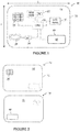
- the Figure 1 shows a smart card 10 which constitutes an example of an integrated circuit card.
- the components shown in dotted lines are generally hidden in the card body 12 while the components shown in solid lines are visible.
- the card can be intended for access to services (payment, telephone, transport).
- the smart card 10 of width l and length L, therefore comprises a plastic card body 12, a main surface of which (here front face) 14 generally comprises graphic prints.
- Card 10 can be in 1FF format within the meaning of ISO / IEC 7810: 2003, ID-1.
- the card 10 comprises an electronic module 20 and associated memories (RAM, ROM) 22 memorizing code instructions 24 for the operation of the card, in particular an enrollment program.
- RAM random access memory
- ROM read-only memory
- It also comprises one or more interfaces for communications with the outside, in particular a set of terminals or contact pads 26 flush with the upper surface 14 and optionally an antenna 28 controlled by a microcontroller 30 for contactless communication (NFC type).
- NFC type contactless communication
- the interface 26 is preferably in accordance with the ISO / IEC 7816-2 standard, for example in its 2007 version.
- the interface 26 is composed of eight electrical contacts distributed in a matrix pattern of two columns of four rows. Each matrix position corresponds to an electrical contact position denoted c1 to c8 according to the standard. Traditionally, the contacts c1 and c5 of the first line are used for supplying the card while the contacts c4 and c8 are not used.
- the 28-30 interface conforms to ISO / IEC 14443.
- Code 24 instructions can then be executed automatically or on command.
- the card 10 also comprises one or more biometric sensors 40 and optionally one or more user interfaces 32, typically LEDs and / or a display, to inform the user of different states or information of the card.
- the various components are interconnected by one or more computer buses.
- the biometric sensor 40 comprises an acquisition zone 42, generally flush with the upper surface 14 of the card 10.
- the biometric sensor 40 is a capacitive fingerprint sensor, for example manufactured according to the method described in the publication FR 3 061 333 A1 .
- the capacitive sensor 40 is formed of an area 42 of pixels.
- biometric sensors can be used, for example in a non-exhaustive way an optical sensor, a luminescence sensor, a multispectral imaging sensor, a thermal sensor, an ultrasonic sensor.
- the Figure 2 shows a similar card 10, the biometric sensor 40 of which is provided on the rear face 16 (opposite the main surface 14 carrying the contact pads 26) of the card body 12.
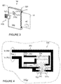
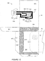
- the Figure 3 shows an enrollment case 50 and a smart card 10 inserted therein through a slot 51.
- the smart card 10 is in position for enrollment.
- such a case can be used for other operations using the card 10 than the simple enrollment taken here by way of illustration.
- the case is formed from a semi-rigid pouch 500 made from a material of vegetable cellulose fibers, typically cardboard.
- the pocket is of the dimensions allowing the card 10 to be inserted therein through the slot 51. It is formed of two panels of similar dimensions, one forming the front face 510 and the other forming the rear face 520, made integral with each other. the other, for example by gluing flaps on three of their sides. The last side, not glued, is formed by the insertion slot 51.
- the panels can be personalized on their external face (as opposed to the inside of the case) by simply printing on the cardboard, in particular the rear panel 520, to place a logo or instructions to follow for the enrollment operations. .
- the biometric sensor 40 is accessible from outside the case 50 allowing the user to use the sensor during enrollment.
- the board 10 can be powered by a 3 to 5V power source either internal or external via a power supply interface 530, here shown as a USB male plug extending from a glued edges of the pocket 500.
- the card 10 When the case 50 is inserted, through the interface 530, into a corresponding powered outlet, the card 10 is powered by an electrical circuit deposited directly into the cellulosic fiber material of the sleeve which electrically connects the electrical contacts 26 of the card 10 to the power supply interface 530 when the card is inserted in the enrollment position.
- the Figure 4 illustrates an example of an electrical circuit 550 allowing this electrical connection between the contacts 26 and the interface 530.
- the electrical circuit 550 is printed on the internal or internal face of one of the panels.
- the Figure 4 shows the print on the inside 510 INT of the 510 front panel. Variations are illustrated below.
- the electrical circuit 550 consists of portions (or segments) of conductive track (black portions) 551 and of electronic components connected to the track, here two LED diodes 552.
- the conductive track portions comprise several contact pads 553 arranged to make contact with the areas 26 of the card 10 as shown in the figure.
- Figure 4a transparent view from the external face of the panel 510) when the card is in the enrollment position.
- the contact pads 553 can be formed by conductive droplets or crimped rivets (in conductive material).
- the pads 553 are arranged in one or more contact positions of a matrix pattern.
- the pattern used is that of the 7816-2: 2007 standard composed of two columns of four rows, corresponding to contacts c1 to c8 (contacts shown in dotted lines).
- the pads 553 opposite the contacts c1 and c5 are directly connected to the track portions VCC and GND of the interface 530 for the purpose of supplying the card 10 when the case 50 is inserted into a power supply device via its interface. 530.
- Other pads 553 can be provided, which allow the enrollment program 24, when it is executed, to control a user interface represented here by the two LEDs 552, also visible on the front panel 510 (see Figure 3 ).
- the user interface 552 can in particular guide the user during the various steps constituting the enrollment operation.
- haptic components based on piezoelectric or PVDF components
- the conductive track portions also include electrical resistors 554 formed of a conductive track.
- the length, width, thickness as well as the material used of the conductive track are determined according to the desired electrical resistance characteristics.
- the electrical resistors 554, formed from the same material as the conductive track portions have a reduced width (compared to adjacent portions 551) and a zig-zag shape.
- the resistors 554 connect the pad 553 for the contact c7 to the two LEDs 552.
- the electric resistors 554 are printed on a zone of the sleeve 500 which is hardly subjected to mechanical torsion, typically remote from the edges of the sleeve (therefore from the edges of the panels forming the faces of the case).
- the power source can be internal to the case 50.
- a power supply interface is therefore provided in the circuit, inside the case. the formed case.
- the power source typically a battery
- the case 50 can be provided, on an external surface of one of the panels 510/520, with a marking indicating where to make a cutout to insert a battery (for example in the form of a button cell) of such so that it is in contact with the internal power supply interface.
- FIGS. 5a to 5c illustrate different variants of the enrollment case 50 according to a first embodiment. These cases differ from each other by the number of openings 511, and their arrangement, made on the front panel 510 between pads 553 to make the movement of these independent and thus guarantee better contact with the contact pads 26 from the menu. Although these variations are illustrated with a USB 530 interface, they also apply to any type of power supply interface.
- the electrical circuit 550 and in particular the contact pads 553 are not shown in transparency for better legibility of the figures.
- the front panel 510 has no opening to the right of the contacts 26 of the card.
- the front panel 510 of the pocket 500 comprises at least one through opening arranged between two contact positions of the matrix pattern, therefore between two pads 553.
- a single elongated vertical opening 511 is provided which separates the pads relating to the two columns of contacts c1-c4 and c5-c8 respectively.
- the length of the through opening 511 is substantially equal to the width I 26 (or height) of the contact module 26 of the card 10.
- the front panel 510 of the pocket comprises a plurality of openings 511 each arranged between two rows, here lines, successive of the matrix pattern carrying contact pads.
- pads are provided on the first three lines corresponding to the contacts c1 / c5, c2 / c6 and c3 / c7 (the contacts c4 and c8 remain unused).
- the openings 511 separate these three lines two by two, giving them freedom of relative movement. Therefore, the cardboard tongue between the two openings 511 has improved flexibility, allowing improved contact of the stud (s) it carries.
- end openings 511e parallel to the openings 511 are provided on the outside of all three lines of the matrix pattern bearing contact pads. This improves the freedom of movement of the two end lines (here those corresponding to c1 / c5 and c3 / c7) relative to the rest of the front panel 510.
- the cardboard tabs between the openings 511 and 511e exhibit flexibility. improved, allowing improved contact of the stud (s) they carry.
- Each opening 511, 511e is through.
- Each opening 511, 511e has a length greater than the distance separating the outer edges of the two contacts (for example c1 and c5) of the same line of the pattern according to the aforementioned standard, that is to say greater than 9.62 mm.
- the length of the openings is less than the width of the contact zone 26 of the card 10. It can however be equal to or greater than it. The length of the opening can therefore be greater than 10 mm, preferably between 12 and 20 mm.
- the plurality of openings comprises at least two distinct openings 511g and 511d separating the contact positions of two successive rows (more generally rows, including the columns) of the matrix pattern.
- at least two (here two) end openings 511eg and 511ed are provided on the same side outside the lines of the matrix pattern carrying contact pads. This makes it possible to improve the independent flexibility of the contact pads of the same line of the matrix pattern.
- pairs of openings are provided instead of a single opening of the Figure 5c .
- the central part of uncut cardboard between the openings of the same pair can be about 1.5 to 2mm.
- the openings 511g, 511d, 511eg and 511ed typically have a length of between 5 and 9.25 mm. In the case of a matrix pattern having more than two contact positions per line, a larger number of openings per line can be provided.
- openings according to the Figure 5c e.g. for end openings 511e
- openings according to Figure 5d for example for the openings 511g, 511d between successive lines carrying contact pads
- Each opening 511, 511e, 511g, 511d, 511eg and 511ed has a width less than the distance separating the center distance of two contacts of two consecutive lines (for example c1 and c2) according to the above-mentioned standard minus the half width of each corresponding stud and the tolerance on the cutout, that is to say typically between 0.1mm and 1mm.
- All the openings made on the same case can have the same dimensions and / or shapes (for example rectangular).
- the Figure 5e illustrates a variant of the Figure 5c where extremal openings 511v perpendicular (here vertical) to the openings 511 are added externally to the whole of the matrix pattern carrying the contact pads.
- extremal openings 511v perpendicular (here vertical) to the openings 511 are added externally to the whole of the matrix pattern carrying the contact pads.
- the 511v vertical end openings can also be combined with the openings of the Figure 5d and / or in the absence of the parallel end openings 511e, 511ed, 511eg.
- the length of the openings 511, 511e is reduced compared to the length.
- the length of the openings 511, 511e is for example between 12 and 16 mm.
- the length of the vertical extremal openings 511v is of the order of magnitude of the height of the contact module 26 of the card, typically 8 to 16 mm for the case of the ISO / IEC 7816-2: 2007 standard.
- FIGS. 5a to 5e show, in hatched parts, guides 521, 522, 523 sandwiched between the front panel 510 and the rear panel 520.
- the guides serve to guide the card 10 towards the enrollment position.
- the guides 521 and 523 include a bevelled portion on the side of the slot 51 towards the interior of the case, thus facilitating the insertion of the card 10 into the case 50.
- the guide 522 provided at the bottom of the pocket relative to the slot 51 acts as a stop means for the card 10 in the enrollment position.
- These guides may be formed by flaps hinged to one or both panels 510, 520 and securing the front panel 510 and the rear panel 520 together.
- the thickness of the flaps makes it possible to produce a spacer between the two panels 510, 520 for the insertion of the card 10.
- the spacer (ideally formed from a single thickness of cardboard with adhesive) is greater than or equal to l maximum thickness of a card as specified in the above-mentioned standard increased by the thickness of the contact pads 530.
- the dimensions of the guides are determined so as to allow the correct positioning of the contacts 26 with respect to the pads 553 in the insertion position (enrollment) of the card 10.
- the dimensions of the panels 510 and 520 are chosen so as to allow, in this position of insertion of the card 10, the biometric sensor 40 to be entirely outside the case 50 and thus be easily accessible to the user.
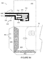
- the Figures 6a to 6d illustrates a method of manufacturing such a case 50 formed in a single piece, in particular in the version illustrated on the Figures 4 , 4a and 5c .
- the blank 600 preferably made of cardboard or any recyclable material, has a thickness of between 0.8 and 1.2 mm allowing the desired spacer to be produced.
- the Figure 6a shows a blank cut in one piece from a single cardboard sheet. It comprises two adjacent and hinged rectangular panels 610 and 620 intended to form the two sides / panels 510 and 520 of the case 50 when they are folded over one another along a common edge forming a joint 699 ( joints are generally shown as broken lines). Edges 61 (of the panels) orthogonal to the hinge 699 define the edges of the insertion slot 51, when the panels are folded back.
- a tongue 630 formed integrally with the panel 610, extends perpendicularly to the first panel 610 on the edge opposite the edge 61 forming a slot 51, on a first portion 631 hinged to a longer end portion 632.
- the two portions 631 and 632 are articulated by a common edge.
- the tab 630 is intended to form the power interface 530 (in the case of an external power source). To do this, the end portion 632 is intended to be folded over and glued to the back of the portion 631 in order to confer rigidity to the interface 630.
- the width of the tongue 630 advantageously corresponds to the width of a USB male plug.
- the thickness of the two glued portions corresponds to the thickness of the internal support of a male USB connector. If this is not the case, other portions, possibly articulated (folded and then glued) and formed in the same piece of cardboard, can be provided to obtain the desired thickness.
- the second panel 620 comprises three articulated flaps 621, 622, 623 extending on the two edges other than the articulation 699 and the edge 61 forming a slot 51, which when they are folded make it possible to maintain, by gluing (preferably both sides), the two panels 610 and 620 together to form the case 50 with the desired spacer.
- these flaps form guides 521, 522, 523 as explained above.
- the articulation 699 and the articulated flaps 622 and 623 make it possible to close the blank 600 in a pocket 500 having the desired spacer and a slot 51 formed by the edges 61 of the two panels.
- the flap 621 has an edge in the continuity of the articulation 699. This edge is perpendicular to the articulation of the flap 621 with the second panel 620. Thus in the folded position of the flap, this edge is aligned with the reinforcing articulation 699 the latter.
- the flaps 621 and 623 make it possible, in particular by their bevelled ends on the side of the edge 61 forming a slot 51, to facilitate the insertion of the card 10 into the case 50 (see Figure 5c ).
- the flaps 621 and 623 may be provided connected, hinged, to the first panel 610 in symmetrical configurations (with respect to the hinge 699) to what is described above.
- the Figure 6b shows the deposition of the portions of conductive track 551 (including resistors 554) directly on the cardboard blank 600, in particular on one side of the blank 600, in particular on one side of the panel 610 intended to form the inner side 510 INT of the front panel 510. Printing on one side of the blank only has a design cost advantage.
- These track portions 551 are formed at the location provided so that the pads 553 finally formed are positioned in line with the corresponding contacts 26 of the card 10, when the latter is in the insertion position (see Figure 4a ).
- the VCC and GND feed track portions extend to the portions 631 and 632 of the tongue 630 forming the power supply interface 530.
- the spacing and width of the track portions at this location conform to the interface. desired, for example in USB format.
- the VCC and GND track portions of the end portion 632 are advantageously oriented on the front face of the case 50 (see Figure 5c ) for a bet in electrical contact with a female USB socket from an external source.
- the biometric sensor 40 of the Figure 1
- the LEDs 552 are easily accessible on the top of the card 10 thus positioned in the case 50.
- the pads 553 are formed at the locations provided, for example by bonding conductive balls using a conductive adhesive, by printing an extra thickness (3D) of conductive material (typically droplets) or by fixing crimped rivets.
- 3D extra thickness
- the Figure 6c shows the next step consisting in making the through openings 511, 511e at the appropriate locations relative to the contacts 26 of a card 10 inserted in the enrollment position.
- one embodiment provides for the production of four identical rectangular openings on either side of the three lines c1 / c5, c2 / c6 and c3 / c7 of the ISO 7816 format.
- the cardboard areas bearing the studs 553 facing each other of these lines are thus advantageously provided with an elasticity facilitating the electrical contact of the pads with the contacts 26.
- other arrangements of openings can be implemented depending on the desired case.
- holes 652 are made in the panel 610 at the locations provided for the LEDs 552. These holes are preferably of smaller diameter than that of the diodes 552 so that the latter are held in the pocket 500 by the periphery of the holes.
- Clearance holes 662 for the diodes are also provided on the flap 622 in line with the holes 652 once the flap 622 is folded and the case 50 has been formed ( Figure 5c ). These holes have a diameter greater than the dimensions of the diodes 552 so as to form a cavity for them in the formed case 50, without being crushed by the flap 622.
- the next step illustrated by Figure 6d consists of inserting diodes 552 into circuit 500.
- LEDs 552 are glued using an adhesive conductor in order to promote the electrical contact of their terminals with the portions of conductive track 551.
- a drop of epoxy-based resin can be deposited (a so-called “globtop” technique) on the diodes 552 to protect them and for better mechanical strength.
- a filling under or on the diodes 552 using an epoxy resin can be considered for better mechanical strength.
- the case 50 obtained ( Figures 3 and 5c ) is self-supporting (without breaking or bending) when the card 10 is inserted into it.
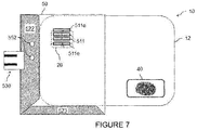
- FIG. 7 illustrates a variant of Figure 5c by the presence of openings 511 and 511e. This variant is also applicable to the cases of Figures 5a , 5b , 5d and 5th .
- the guide flap 621 at the level of the articulation between the panels 610, 620 forming the faces of the case is not provided, making it possible to simplify the design steps of the blank 600 and the folding and gluing steps to form the case 50.
- the fold along the edge 699 then performs the function of guiding the card 10 (in addition to the flaps 622 and 623 remaining).
- FIGS. 8a to 8d illustrate a method of manufacturing this case 50.
- the explanations provided above in connection with the Figures 6a to 6d apply, except for flap 621.
- the Figure 9 illustrates a variant of the Figure 6d during the manufacturing process of a case 50 in accordance with Figure 5a , 5b , 5c , 5d or 5c (by adapting the number of openings 511, 511e, 511d, 511g, 511ed, 511eg and their arrangement).
- the different stages corresponding to Figures 6a to 6c are not shown to simplify the presentation. However, they can be deduced in the light of the Figure 9 .
- the tab 630 forming the power supply interface 530 extends from the second panel 620, similarly to what has been described in connection with the Figure 6a .
- the circuit 550 which is mainly printed on the inner face of the first panel 610 is extended by two portions of conductive track VCC and GND up to the first portion 631 of the tongue 630.
- This arrangement does not require the extension of these.
- two track portions up to the end portion 632 of the tongue because the electrical contact with a female USB socket will be made through the upper zone (here visible) of the first portion 631 of the tongue.
- the result is the absence of a point of weakness in these portions of the track at the fold between the two portions 631 and 632 of the tongue.
- the end portion 632 of the tongue is intended to be folded over and be glued to the back of the first portion 631 for the purpose of imparting rigidity and sufficient thickness to the power supply interface 530.
- other portions can be provided. which are folded and glued, in order to obtain a sufficient number of layers to achieve the desired thickness.
- the extension of the conductive track portions between the two panels is produced on the same face of the two panels 610 and 620, simplifying the manufacturing process.
- a stretchable ink in particular based on silver, is preferably used for their preparation. This improves the reliability of the conductive track portions.
- these portions of conductive track are printed in zigzag fashion at the edges (only) of the fold, which improves the elastic resistance of the ink.
- the conductive track portions deposited on the second panel 620 are preferably produced in the part of the panel reserved for folding and gluing the flaps 621 and 622 (that is to say the hatched areas 521 and 522 in the Figure). In this case, these track portions are not liable to be altered by friction against the card 10 when the latter is introduced into the case 50 formed from the blank 600.
- the three flaps 621, 622, 623 are still provided to close the case 50 and guide the card 10 which is introduced therein through the slot 51.
- the case bottom flap 622 50 is connected, hinged, to the first panel 610, due to the presence of the tongue 630 on the second panel 620.
- the flap 621 can be interconnected, hinged, to the first panel 610 (as illustrated) or to the second panel 620 (as on the Figures 6 ), in the vicinity of articulation 699.
- the flap 621 parallel to the articulation 699 is arranged at a distance ⁇ from the articulation 699.
- contact pads can be provided on these portions of the track in the vicinity of the articulation 699 (on one side or on both sides of the articulation) in order to make the contact of the same portion of the track on both sides more reliable. other of joint 699.
- the flap 623 can be interconnected, hinged, to the first panel 610 (as illustrated) or to the second panel 620 (as on the Figures 6 ).
- the flaps 621 and 623 notably comprise ends bevelled towards the inside of the side of the edge 61 forming a slot 51, in order to facilitate the insertion of the card 10 into the case 50.
- the fold 699 acts as a guide for the card 10 when it is introduced through the slot 51, instead of the flap 621.
- FIGs 11a and 11b illustrate another embodiment of a case 50 for use with a card according to Figure 2 , that is to say provided with a biometric sensor 40 on the lower face 16 (opposite to that 14 carrying the contacts 26).
- VCC and GND track portions are provided on the same side of the case 50 as that where the biometric sensor 40 of the card 10 will be accessible once the latter has been inserted ( Figure 11b ).
- the diodes 552 are visible on the other side of the case 50 ( Figure 11a ). In a variant, the diodes 552 are visible on the same side as the biometric sensor 40, the one shown Figure 11b .
- the Figure 12 illustrates an example of blank 600 corresponding to the case of Figures 11a and 11b .
- This Figure represents the blank during the last stage of constitution of the case 50.
- the various preliminary stages corresponding to the Figures 6a / 8a to 6c / 8c are not shown to simplify the presentation. However, they can be deduced in the light of the Figure 12 .
- the electrical circuit 550 is deposited on a single face of a single panel, here the first panel 610. As visible in the Figure, the electrical circuit is compact. The conductive track portions 551 do not pass through any bending zone, reducing the risks of malfunction.
- the perforations 652 can be made in the second panel 620 (and not in the first panel ) and the diodes 552 can be turned over to engage these perforations of the second panel 620 when the case 50 is closed. These perforations are illustrated by white dotted circles.
- the flaps 621 and 623 can be interconnected, hinged, to the first panel 610 or to the second panel 620 (as illustrated).
- the flaps 621 and 623 notably include bevelled ends on the side of the edge 61 forming a slot 51 (as described above), in order to facilitate the insertion of the card 10 into the case 50.
- the flap 621 is optional. In its absence, the fold 699 acts as a guide for the card 10 when it is inserted into the case 50.
- the Figures 10 and 12 are applicable for the manufacture of a case comprising an arrangement of openings other than that illustrated (four openings as in Figure 5c ), especially the layouts of Figures 5a (no opening), 5b, 5d and 5th.
- the above examples are based on the use of a single cardboard blank 600 (or equivalent) to form, by folding and gluing, the case 50.
- the case 50 can be constituted by gluing of several independent cardboard pieces (or equivalent), with possible folds.
- openings 511 While some arrangements of openings 511 are described and illustrated, the invention applies to other arrangements, including openings of the same or different dimensions.
Landscapes
- Engineering & Computer Science (AREA)
- Physics & Mathematics (AREA)
- Theoretical Computer Science (AREA)
- Computer Hardware Design (AREA)
- General Physics & Mathematics (AREA)
- Microelectronics & Electronic Packaging (AREA)
- Computer Security & Cryptography (AREA)
- General Engineering & Computer Science (AREA)
- Computer Vision & Pattern Recognition (AREA)
- Artificial Intelligence (AREA)
- Business, Economics & Management (AREA)
- Software Systems (AREA)
- Electromagnetism (AREA)
- Automation & Control Theory (AREA)
- Computer Networks & Wireless Communication (AREA)
- Accounting & Taxation (AREA)
- Strategic Management (AREA)
- General Business, Economics & Management (AREA)
- Details Of Connecting Devices For Male And Female Coupling (AREA)
- Cartons (AREA)
- Credit Cards Or The Like (AREA)
Applications Claiming Priority (1)
| Application Number | Priority Date | Filing Date | Title |
|---|---|---|---|
| FR1904662A FR3095735B1 (fr) | 2019-05-03 | 2019-05-03 | Etui d’enrôlement pour carte à puce |
Publications (3)
| Publication Number | Publication Date |
|---|---|
| EP3734493A1 true EP3734493A1 (de) | 2020-11-04 |
| EP3734493C0 EP3734493C0 (de) | 2023-06-07 |
| EP3734493B1 EP3734493B1 (de) | 2023-06-07 |
Family
ID=67262756
Family Applications (1)
| Application Number | Title | Priority Date | Filing Date |
|---|---|---|---|
| EP20166518.9A Active EP3734493B1 (de) | 2019-05-03 | 2020-03-27 | Aufnahmeetui für chipkarte |
Country Status (6)
| Country | Link |
|---|---|
| US (1) | US11068766B2 (de) |
| EP (1) | EP3734493B1 (de) |
| JP (1) | JP7526581B2 (de) |
| KR (1) | KR102756640B1 (de) |
| CN (1) | CN111882016A (de) |
| FR (1) | FR3095735B1 (de) |
Cited By (1)
| Publication number | Priority date | Publication date | Assignee | Title |
|---|---|---|---|---|
| FR3116138A1 (fr) * | 2020-11-12 | 2022-05-13 | Stmicroelectronics (Rousset) Sas | Dispositif pour l'enrôlement d'une carte à microcircuit |
Families Citing this family (6)
| Publication number | Priority date | Publication date | Assignee | Title |
|---|---|---|---|---|
| EP3923196A1 (de) * | 2020-06-09 | 2021-12-15 | Thales Dis France Sa | Verfahren zur herstellung einer hochfrequenz-chipkarte mit einer metallischen einlagenanordnung |
| US12380308B2 (en) | 2022-01-10 | 2025-08-05 | Fingerprint Cards Anacatum Ip Ab | Enrollment assistance device with electronic label, and manufacturing method |
| WO2023249539A1 (en) * | 2022-06-23 | 2023-12-28 | Fingerprint Cards Anacatum Ip Ab | Enrollment assistance device with conductor spiral, biometric system and enrollment method |
| EP4296887B1 (de) * | 2022-06-23 | 2024-06-26 | Fingerprint Cards Anacatum IP AB | Registrierungshilfsvorrichtung mit kapazitiven koppelpads, biometrisches system und registrierungsverfahren |
| WO2024128955A1 (en) * | 2022-12-12 | 2024-06-20 | Fingerprint Cards Anacatum Ip Ab | Enrollment assistance device and method of biometrically enrolling a user |
| US12488204B1 (en) * | 2024-12-24 | 2025-12-02 | Magic Control Technology Corporation | Card reader |
Citations (3)
| Publication number | Priority date | Publication date | Assignee | Title |
|---|---|---|---|---|
| EP1222623A1 (de) * | 1999-09-30 | 2002-07-17 | Moore Corporation Limited | Billiges lesen von rf-etiketten über grosse entfernungen |
| FR3061333A1 (fr) | 2016-12-26 | 2018-06-29 | Oberthur Technologies | Carte plastique mince integrant un capteur d'empreinte digitale et procede de realisation |
| US20180276518A1 (en) | 2017-03-23 | 2018-09-27 | Idex Asa | Sensor array system selectively configurable as a fingerprint sensor or data entry device |
Family Cites Families (24)
| Publication number | Priority date | Publication date | Assignee | Title |
|---|---|---|---|---|
| US5380695A (en) * | 1994-04-22 | 1995-01-10 | Polaroid Corporation | Image-receiving element for thermal dye transfer method |
| FR2742561B1 (fr) * | 1995-12-13 | 1998-01-09 | Itt Composants Instr | Connecteur electrique pour une carte a circuit(s) integre(s) a contact |
| JPH10121395A (ja) * | 1996-10-15 | 1998-05-12 | Oji Paper Co Ltd | 剛度と嵩高性に優れた紙 |
| NZ517720A (en) * | 1999-09-07 | 2004-03-26 | American Express Travel Relate | Transaction card |
| WO2003056499A2 (en) * | 2001-12-24 | 2003-07-10 | Digimarc Id Systems Llc | Pet based multi-multi-layer smart cards |
| JP4240989B2 (ja) * | 2002-10-15 | 2009-03-18 | 大日本印刷株式会社 | 3種のインターフェースを備えるicモジュール、3ウェイsimとsimホルダー、3ウェイicカードとicカードホルダー |
| JP2004170548A (ja) * | 2002-11-18 | 2004-06-17 | Fuji Photo Film Co Ltd | 表面処理装置及び画像形成装置 |
| JP2004234254A (ja) * | 2003-01-29 | 2004-08-19 | Dainippon Printing Co Ltd | Icカード用リーダライタ |
| ATE394243T1 (de) * | 2003-02-27 | 2008-05-15 | Landqart | Mehrschichtlaminat |
| JP2004265166A (ja) * | 2003-03-03 | 2004-09-24 | Dainippon Printing Co Ltd | Icカード用リーダライタ |
| US20050139685A1 (en) * | 2003-12-30 | 2005-06-30 | Douglas Kozlay | Design & method for manufacturing low-cost smartcards with embedded fingerprint authentication system modules |
| JP4138732B2 (ja) | 2004-11-17 | 2008-08-27 | セイコーエプソン株式会社 | カードケース |
| US20060113381A1 (en) * | 2004-11-29 | 2006-06-01 | John Hochstein | Batteryless contact fingerprint-enabled smartcard that enables contactless capability |
| DE602007013478D1 (de) * | 2006-02-08 | 2011-05-12 | Semiconductor Energy Lab | RFID-Vorrichtung |
| US8240022B2 (en) * | 2006-09-26 | 2012-08-14 | Feinics Amatech Teorowita | Methods of connecting an antenna to a transponder chip |
| JP4418504B2 (ja) * | 2008-07-08 | 2010-02-17 | 一紀 山形 | 非接触式icカードホルダー |
| FR2935060B1 (fr) * | 2008-08-12 | 2010-09-10 | Arjowiggins Licensing Sas | E-document comportant un element de perturbation electromagnetique |
| GB2531607B (en) * | 2014-10-24 | 2018-04-18 | Novalia Ltd | Article incorporating a capacitive touch device and having a non-flat surface |
| US20160159557A1 (en) * | 2014-12-09 | 2016-06-09 | Maui Kahawaiolaa | Cigarette Packaging, and Method for Sealing a Cigarette Package |
| DE102015222364A1 (de) * | 2015-11-12 | 2017-05-18 | Bundesdruckerei Gmbh | Wert- oder Sicherheitsdokument aus einem Faserverbundwerkstoff und Verfahren zum Herstellen des Wert- oder Sicherheitsdokuments |
| US9900984B2 (en) * | 2015-12-31 | 2018-02-20 | Taisys Technologies Co. Ltd. | Auxiliary mounting structure for mounting advanced smart card |
| EP3251972B1 (de) * | 2016-05-31 | 2018-08-01 | Philip Morris Products S.a.s. | Behälter mit mitteln zum verbesserten verschluss, verfahren |
| US10640925B2 (en) * | 2017-02-15 | 2020-05-05 | Flex R&D Inc. | Lightweight paper board |
| US10694361B2 (en) * | 2018-10-11 | 2020-06-23 | International Business Machines Corporation | Computer-implemented agent assisted electronic business cards |
-
2019
- 2019-05-03 FR FR1904662A patent/FR3095735B1/fr active Active
-
2020
- 2020-03-27 EP EP20166518.9A patent/EP3734493B1/de active Active
- 2020-04-14 JP JP2020072309A patent/JP7526581B2/ja active Active
- 2020-04-28 CN CN202010347500.8A patent/CN111882016A/zh active Pending
- 2020-04-28 US US16/860,571 patent/US11068766B2/en active Active
- 2020-04-29 KR KR1020200052129A patent/KR102756640B1/ko active Active
Patent Citations (3)
| Publication number | Priority date | Publication date | Assignee | Title |
|---|---|---|---|---|
| EP1222623A1 (de) * | 1999-09-30 | 2002-07-17 | Moore Corporation Limited | Billiges lesen von rf-etiketten über grosse entfernungen |
| FR3061333A1 (fr) | 2016-12-26 | 2018-06-29 | Oberthur Technologies | Carte plastique mince integrant un capteur d'empreinte digitale et procede de realisation |
| US20180276518A1 (en) | 2017-03-23 | 2018-09-27 | Idex Asa | Sensor array system selectively configurable as a fingerprint sensor or data entry device |
Non-Patent Citations (2)
| Title |
|---|
| CARUSO FRANCESCO ET AL: "High-throughput shadow mask printing of passive electrical components on paper by supersonic cluster beam deposition", APPLIED PHYSICS LETTERS, A I P PUBLISHING LLC, US, vol. 108, no. 16, 18 April 2016 (2016-04-18), XP012207002, ISSN: 0003-6951, [retrieved on 19010101], DOI: 10.1063/1.4947281 * |
| CLAUDIA DAUDÉN ROQUET ET AL: "3D Folded PrintGami", DESIGNING INTERACTIVE SYSTEMS, ACM, 2 PENN PLAZA, SUITE 701 NEW YORK NY 10121-0701 USA, 4 June 2016 (2016-06-04), pages 187 - 191, XP058259394, ISBN: 978-1-4503-4031-1, DOI: 10.1145/2901790.2901891 * |
Cited By (3)
| Publication number | Priority date | Publication date | Assignee | Title |
|---|---|---|---|---|
| FR3116138A1 (fr) * | 2020-11-12 | 2022-05-13 | Stmicroelectronics (Rousset) Sas | Dispositif pour l'enrôlement d'une carte à microcircuit |
| EP4002194A1 (de) * | 2020-11-12 | 2022-05-25 | STMicroelectronics (Rousset) SAS | Vorrichtung zur erfassung einer mikroschaltkreiskarte |
| US11954548B2 (en) | 2020-11-12 | 2024-04-09 | STMicroelectronics (Grand Ouest) SAS | Smart card enrollment device |
Also Published As
| Publication number | Publication date |
|---|---|
| EP3734493C0 (de) | 2023-06-07 |
| CN111882016A (zh) | 2020-11-03 |
| KR20200127889A (ko) | 2020-11-11 |
| US20200349408A1 (en) | 2020-11-05 |
| KR102756640B1 (ko) | 2025-01-16 |
| JP7526581B2 (ja) | 2024-08-01 |
| FR3095735A1 (fr) | 2020-11-06 |
| EP3734493B1 (de) | 2023-06-07 |
| US11068766B2 (en) | 2021-07-20 |
| JP2020184328A (ja) | 2020-11-12 |
| FR3095735B1 (fr) | 2021-05-21 |
Similar Documents
| Publication | Publication Date | Title |
|---|---|---|
| EP3734493B1 (de) | Aufnahmeetui für chipkarte | |
| EP1810227B1 (de) | Personalisierte elektronische usb-schlüssel-vorrichtung und verfahren zu ihrer herstellung | |
| EP3432221B1 (de) | Elektronische karte, die einen fingerabdrucksensor umfasst, und herstellungsverfahren einer solchen karte | |
| EP1433125B1 (de) | Mit einem port einer telekommunikationseinrichtung zu verbindendes dongle | |
| FR2936072A1 (fr) | Dispositif electronique portable a connecteur usb. | |
| EP2047414B1 (de) | Sicheres dokument, insbesondere elektronischer pass mit verbesserter sicherheit | |
| EP3223199B1 (de) | Herstellungsverfahren eines multifunktionsmoduls, und dieses modul umfassende vorrichtung | |
| EP3920091B1 (de) | Biometrisches sensormodul für chipkarte und verfahren zur herstellung eines solchen moduls | |
| WO2012168666A1 (fr) | Module a microcircuit et carte a puce le comportant | |
| EP2239691B1 (de) | Einheit mit Speicherschlüssel, der eine Chipkarte umfasst | |
| EP0980561B1 (de) | Entfernbare karte mit einer steckverbindung als smartkartenleser für einen mikrocomputer | |
| EP2045765B1 (de) | Verfahren zur Herstellung eines elektronischen Schlüssels mit USB-Stecker | |
| EP2933759A1 (de) | Herstellungsverfahren einer Vorrichtung mit elektronischem/elektrischem Schaltkreis | |
| WO2013072616A1 (fr) | Ensemble comportant un adaptateur et une carte a puce | |
| EP2439079A1 (de) | Sicherheitsdokument, das eine Kommunikationsvorrichtung im nahen Umfeld umfasst, wie etwa einen Reisepass | |
| EP1843277A1 (de) | USB-Chipkarte | |
| EP3452958B1 (de) | Verfahren zur herstellung von chipkarten und durch besagtes verfahren erhaltene chipkarte | |
| WO1999060518A1 (fr) | Support pour un circuit electronique, comprenant des moyens anti-arrachement | |
| WO2021223884A1 (fr) | Carte en métal et coque associée | |
| EP2765536A1 (de) | Verfahren zur Verbindung eines Mikroschaltkreises mit leitenden Zonen, die in einem Träger zugänglich sind | |
| EP2293226B1 (de) | Elektronische Vorrichtung, die eine Mikrochip-Karte umfasst | |
| EP3471024A1 (de) | Chipkarte mit gesichertem elektronischen modul, und ihr herstellungsverfahren | |
| WO2014060290A1 (fr) | Procede de fabrication d'un dispositif multi-composants comprenant un module electrique et/ou electronique | |
| FR3058085A1 (fr) | Procede pour realiser un contour de document de securite personnalise |
Legal Events
| Date | Code | Title | Description |
|---|---|---|---|
| PUAI | Public reference made under article 153(3) epc to a published international application that has entered the european phase |
Free format text: ORIGINAL CODE: 0009012 |
|
| STAA | Information on the status of an ep patent application or granted ep patent |
Free format text: STATUS: THE APPLICATION HAS BEEN PUBLISHED |
|
| AK | Designated contracting states |
Kind code of ref document: A1 Designated state(s): AL AT BE BG CH CY CZ DE DK EE ES FI FR GB GR HR HU IE IS IT LI LT LU LV MC MK MT NL NO PL PT RO RS SE SI SK SM TR |
|
| AX | Request for extension of the european patent |
Extension state: BA ME |
|
| STAA | Information on the status of an ep patent application or granted ep patent |
Free format text: STATUS: REQUEST FOR EXAMINATION WAS MADE |
|
| 17P | Request for examination filed |
Effective date: 20210330 |
|
| RBV | Designated contracting states (corrected) |
Designated state(s): AL AT BE BG CH CY CZ DE DK EE ES FI FR GB GR HR HU IE IS IT LI LT LU LV MC MK MT NL NO PL PT RO RS SE SI SK SM TR |
|
| STAA | Information on the status of an ep patent application or granted ep patent |
Free format text: STATUS: EXAMINATION IS IN PROGRESS |
|
| 17Q | First examination report despatched |
Effective date: 20210705 |
|
| GRAP | Despatch of communication of intention to grant a patent |
Free format text: ORIGINAL CODE: EPIDOSNIGR1 |
|
| STAA | Information on the status of an ep patent application or granted ep patent |
Free format text: STATUS: GRANT OF PATENT IS INTENDED |
|
| INTG | Intention to grant announced |
Effective date: 20221010 |
|
| GRAS | Grant fee paid |
Free format text: ORIGINAL CODE: EPIDOSNIGR3 |
|
| GRAA | (expected) grant |
Free format text: ORIGINAL CODE: 0009210 |
|
| STAA | Information on the status of an ep patent application or granted ep patent |
Free format text: STATUS: THE PATENT HAS BEEN GRANTED |
|
| AK | Designated contracting states |
Kind code of ref document: B1 Designated state(s): AL AT BE BG CH CY CZ DE DK EE ES FI FR GB GR HR HU IE IS IT LI LT LU LV MC MK MT NL NO PL PT RO RS SE SI SK SM TR |
|
| REG | Reference to a national code |
Ref country code: GB Ref legal event code: FG4D Free format text: NOT ENGLISH |
|
| REG | Reference to a national code |
Ref country code: CH Ref legal event code: EP Ref country code: AT Ref legal event code: REF Ref document number: 1577196 Country of ref document: AT Kind code of ref document: T Effective date: 20230615 Ref country code: DE Ref legal event code: R096 Ref document number: 602020011505 Country of ref document: DE |
|
| U01 | Request for unitary effect filed |
Effective date: 20230607 |
|
| U07 | Unitary effect registered |
Designated state(s): AT BE BG DE DK EE FI FR IT LT LU LV MT NL PT SE SI Effective date: 20230612 |
|
| REG | Reference to a national code |
Ref country code: LT Ref legal event code: MG9D |
|
| PG25 | Lapsed in a contracting state [announced via postgrant information from national office to epo] |
Ref country code: NO Free format text: LAPSE BECAUSE OF FAILURE TO SUBMIT A TRANSLATION OF THE DESCRIPTION OR TO PAY THE FEE WITHIN THE PRESCRIBED TIME-LIMIT Effective date: 20230907 Ref country code: ES Free format text: LAPSE BECAUSE OF FAILURE TO SUBMIT A TRANSLATION OF THE DESCRIPTION OR TO PAY THE FEE WITHIN THE PRESCRIBED TIME-LIMIT Effective date: 20230607 |
|
| PG25 | Lapsed in a contracting state [announced via postgrant information from national office to epo] |
Ref country code: RS Free format text: LAPSE BECAUSE OF FAILURE TO SUBMIT A TRANSLATION OF THE DESCRIPTION OR TO PAY THE FEE WITHIN THE PRESCRIBED TIME-LIMIT Effective date: 20230607 Ref country code: HR Free format text: LAPSE BECAUSE OF FAILURE TO SUBMIT A TRANSLATION OF THE DESCRIPTION OR TO PAY THE FEE WITHIN THE PRESCRIBED TIME-LIMIT Effective date: 20230607 Ref country code: GR Free format text: LAPSE BECAUSE OF FAILURE TO SUBMIT A TRANSLATION OF THE DESCRIPTION OR TO PAY THE FEE WITHIN THE PRESCRIBED TIME-LIMIT Effective date: 20230908 |
|
| PG25 | Lapsed in a contracting state [announced via postgrant information from national office to epo] |
Ref country code: SK Free format text: LAPSE BECAUSE OF FAILURE TO SUBMIT A TRANSLATION OF THE DESCRIPTION OR TO PAY THE FEE WITHIN THE PRESCRIBED TIME-LIMIT Effective date: 20230607 |
|
| PG25 | Lapsed in a contracting state [announced via postgrant information from national office to epo] |
Ref country code: IS Free format text: LAPSE BECAUSE OF FAILURE TO SUBMIT A TRANSLATION OF THE DESCRIPTION OR TO PAY THE FEE WITHIN THE PRESCRIBED TIME-LIMIT Effective date: 20231007 |
|
| PG25 | Lapsed in a contracting state [announced via postgrant information from national office to epo] |
Ref country code: SM Free format text: LAPSE BECAUSE OF FAILURE TO SUBMIT A TRANSLATION OF THE DESCRIPTION OR TO PAY THE FEE WITHIN THE PRESCRIBED TIME-LIMIT Effective date: 20230607 Ref country code: SK Free format text: LAPSE BECAUSE OF FAILURE TO SUBMIT A TRANSLATION OF THE DESCRIPTION OR TO PAY THE FEE WITHIN THE PRESCRIBED TIME-LIMIT Effective date: 20230607 Ref country code: RO Free format text: LAPSE BECAUSE OF FAILURE TO SUBMIT A TRANSLATION OF THE DESCRIPTION OR TO PAY THE FEE WITHIN THE PRESCRIBED TIME-LIMIT Effective date: 20230607 Ref country code: IS Free format text: LAPSE BECAUSE OF FAILURE TO SUBMIT A TRANSLATION OF THE DESCRIPTION OR TO PAY THE FEE WITHIN THE PRESCRIBED TIME-LIMIT Effective date: 20231007 Ref country code: CZ Free format text: LAPSE BECAUSE OF FAILURE TO SUBMIT A TRANSLATION OF THE DESCRIPTION OR TO PAY THE FEE WITHIN THE PRESCRIBED TIME-LIMIT Effective date: 20230607 |
|
| PG25 | Lapsed in a contracting state [announced via postgrant information from national office to epo] |
Ref country code: PL Free format text: LAPSE BECAUSE OF FAILURE TO SUBMIT A TRANSLATION OF THE DESCRIPTION OR TO PAY THE FEE WITHIN THE PRESCRIBED TIME-LIMIT Effective date: 20230607 |
|
| REG | Reference to a national code |
Ref country code: DE Ref legal event code: R097 Ref document number: 602020011505 Country of ref document: DE |
|
| U20 | Renewal fee for the european patent with unitary effect paid |
Year of fee payment: 5 Effective date: 20240220 |
|
| PLBE | No opposition filed within time limit |
Free format text: ORIGINAL CODE: 0009261 |
|
| STAA | Information on the status of an ep patent application or granted ep patent |
Free format text: STATUS: NO OPPOSITION FILED WITHIN TIME LIMIT |
|
| 26N | No opposition filed |
Effective date: 20240308 |
|
| REG | Reference to a national code |
Ref country code: CH Ref legal event code: PL |
|
| PG25 | Lapsed in a contracting state [announced via postgrant information from national office to epo] |
Ref country code: MC Free format text: LAPSE BECAUSE OF FAILURE TO SUBMIT A TRANSLATION OF THE DESCRIPTION OR TO PAY THE FEE WITHIN THE PRESCRIBED TIME-LIMIT Effective date: 20230607 |
|
| GBPC | Gb: european patent ceased through non-payment of renewal fee |
Effective date: 20240327 |
|
| PG25 | Lapsed in a contracting state [announced via postgrant information from national office to epo] |
Ref country code: MC Free format text: LAPSE BECAUSE OF FAILURE TO SUBMIT A TRANSLATION OF THE DESCRIPTION OR TO PAY THE FEE WITHIN THE PRESCRIBED TIME-LIMIT Effective date: 20230607 |
|
| PG25 | Lapsed in a contracting state [announced via postgrant information from national office to epo] |
Ref country code: GB Free format text: LAPSE BECAUSE OF NON-PAYMENT OF DUE FEES Effective date: 20240327 |
|
| PG25 | Lapsed in a contracting state [announced via postgrant information from national office to epo] |
Ref country code: IE Free format text: LAPSE BECAUSE OF NON-PAYMENT OF DUE FEES Effective date: 20240327 |
|
| PG25 | Lapsed in a contracting state [announced via postgrant information from national office to epo] |
Ref country code: IE Free format text: LAPSE BECAUSE OF NON-PAYMENT OF DUE FEES Effective date: 20240327 Ref country code: GB Free format text: LAPSE BECAUSE OF NON-PAYMENT OF DUE FEES Effective date: 20240327 Ref country code: CH Free format text: LAPSE BECAUSE OF NON-PAYMENT OF DUE FEES Effective date: 20240331 |
|
| U20 | Renewal fee for the european patent with unitary effect paid |
Year of fee payment: 6 Effective date: 20250210 |
|
| PG25 | Lapsed in a contracting state [announced via postgrant information from national office to epo] |
Ref country code: CY Free format text: LAPSE BECAUSE OF FAILURE TO SUBMIT A TRANSLATION OF THE DESCRIPTION OR TO PAY THE FEE WITHIN THE PRESCRIBED TIME-LIMIT; INVALID AB INITIO Effective date: 20200327 |
|
| PG25 | Lapsed in a contracting state [announced via postgrant information from national office to epo] |
Ref country code: HU Free format text: LAPSE BECAUSE OF FAILURE TO SUBMIT A TRANSLATION OF THE DESCRIPTION OR TO PAY THE FEE WITHIN THE PRESCRIBED TIME-LIMIT; INVALID AB INITIO Effective date: 20200327 |
|
| PG25 | Lapsed in a contracting state [announced via postgrant information from national office to epo] |
Ref country code: TR Free format text: LAPSE BECAUSE OF FAILURE TO SUBMIT A TRANSLATION OF THE DESCRIPTION OR TO PAY THE FEE WITHIN THE PRESCRIBED TIME-LIMIT Effective date: 20230607 |
|
| U1K | Transfer of rights of the unitary patent after the registration of the unitary effect |
Owner name: IDEMIA FRANCE; FR |