EP3736626A1 - Antenne à cristaux liquides et son procédé de fabrication - Google Patents
Antenne à cristaux liquides et son procédé de fabrication Download PDFInfo
- Publication number
- EP3736626A1 EP3736626A1 EP19863991.6A EP19863991A EP3736626A1 EP 3736626 A1 EP3736626 A1 EP 3736626A1 EP 19863991 A EP19863991 A EP 19863991A EP 3736626 A1 EP3736626 A1 EP 3736626A1
- Authority
- EP
- European Patent Office
- Prior art keywords
- substrate
- metal film
- liquid crystal
- layer
- film layer
- Prior art date
- Legal status (The legal status is an assumption and is not a legal conclusion. Google has not performed a legal analysis and makes no representation as to the accuracy of the status listed.)
- Granted
Links
Images


Classifications
-
- G—PHYSICS
- G02—OPTICS
- G02F—OPTICAL DEVICES OR ARRANGEMENTS FOR THE CONTROL OF LIGHT BY MODIFICATION OF THE OPTICAL PROPERTIES OF THE MEDIA OF THE ELEMENTS INVOLVED THEREIN; NON-LINEAR OPTICS; FREQUENCY-CHANGING OF LIGHT; OPTICAL LOGIC ELEMENTS; OPTICAL ANALOGUE/DIGITAL CONVERTERS
- G02F1/00—Devices or arrangements for the control of the intensity, colour, phase, polarisation or direction of light arriving from an independent light source, e.g. switching, gating or modulating; Non-linear optics
- G02F1/01—Devices or arrangements for the control of the intensity, colour, phase, polarisation or direction of light arriving from an independent light source, e.g. switching, gating or modulating; Non-linear optics for the control of the intensity, phase, polarisation or colour
- G02F1/13—Devices or arrangements for the control of the intensity, colour, phase, polarisation or direction of light arriving from an independent light source, e.g. switching, gating or modulating; Non-linear optics for the control of the intensity, phase, polarisation or colour based on liquid crystals, e.g. single liquid crystal display cells
- G02F1/1313—Devices or arrangements for the control of the intensity, colour, phase, polarisation or direction of light arriving from an independent light source, e.g. switching, gating or modulating; Non-linear optics for the control of the intensity, phase, polarisation or colour based on liquid crystals, e.g. single liquid crystal display cells specially adapted for a particular application
-
- H—ELECTRICITY
- H01—ELECTRIC ELEMENTS
- H01Q—ANTENNAS, i.e. RADIO AERIALS
- H01Q1/00—Details of, or arrangements associated with, antennas
- H01Q1/36—Structural form of radiating elements, e.g. cone, spiral, umbrella; Particular materials used therewith
- H01Q1/38—Structural form of radiating elements, e.g. cone, spiral, umbrella; Particular materials used therewith formed by a conductive layer on an insulating support
-
- G—PHYSICS
- G02—OPTICS
- G02F—OPTICAL DEVICES OR ARRANGEMENTS FOR THE CONTROL OF LIGHT BY MODIFICATION OF THE OPTICAL PROPERTIES OF THE MEDIA OF THE ELEMENTS INVOLVED THEREIN; NON-LINEAR OPTICS; FREQUENCY-CHANGING OF LIGHT; OPTICAL LOGIC ELEMENTS; OPTICAL ANALOGUE/DIGITAL CONVERTERS
- G02F1/00—Devices or arrangements for the control of the intensity, colour, phase, polarisation or direction of light arriving from an independent light source, e.g. switching, gating or modulating; Non-linear optics
- G02F1/01—Devices or arrangements for the control of the intensity, colour, phase, polarisation or direction of light arriving from an independent light source, e.g. switching, gating or modulating; Non-linear optics for the control of the intensity, phase, polarisation or colour
- G02F1/13—Devices or arrangements for the control of the intensity, colour, phase, polarisation or direction of light arriving from an independent light source, e.g. switching, gating or modulating; Non-linear optics for the control of the intensity, phase, polarisation or colour based on liquid crystals, e.g. single liquid crystal display cells
- G02F1/133—Constructional arrangements; Operation of liquid crystal cells; Circuit arrangements
- G02F1/1333—Constructional arrangements; Manufacturing methods
- G02F1/1343—Electrodes
- G02F1/13439—Electrodes characterised by their electrical, optical, physical properties; materials therefor; method of making
-
- H—ELECTRICITY
- H01—ELECTRIC ELEMENTS
- H01Q—ANTENNAS, i.e. RADIO AERIALS
- H01Q1/00—Details of, or arrangements associated with, antennas
- H01Q1/36—Structural form of radiating elements, e.g. cone, spiral, umbrella; Particular materials used therewith
- H01Q1/364—Structural form of radiating elements, e.g. cone, spiral, umbrella; Particular materials used therewith using a particular conducting material, e.g. superconductor
Definitions
- the disclosure relates to the technical field of wireless communication, in particular to a liquid crystal antenna and a manufacturing method thereof.
- Antenna as the core equipment for sending and receiving communication information, has become the key factor affecting the performance index of information networks and the application effect of users.
- phased array antenna has this performance index, but based on the national defense application background and chip manufacturing technology, the expensive production cost and high power consumption of the phased array antenna make it unaffordable for consumers in the consumer market, thus causing obstacles to the popularization of consumer products.
- the disclosure provides a liquid crystal antenna, including a first substrate and a second substrate which are oppositely arranged and a liquid crystal layer positioned between the first substrate and the second substrate, wherein a first metal film layer is arranged on one side, facing the second substrate, of the first substrate, a second metal film layer is arranged on one side, facing the first substrate, of the second substrate, the first substrate and the second substrate are rigid substrates, a seed layer is arranged between the first substrate and the first metal film layer, and a seed layer is arranged between the second substrate and the second metal film layer.
- the first metal film layer and the second metal film layer are each a chemically deposited layer laminated on the seed layer of the corresponding substrate.
- the first metal film layer and the second metal film layer are each composed of a chemically deposited layer and an electroplated metal layer which are sequentially laminated on the seed layer of the corresponding substrate.
- the metal materials of the first metal film layer and the second metal film layer are silver, copper, gold, aluminum, or alloys thereof.
- the conductivity of the metal materials is ⁇
- the magnetic permeability is ⁇
- the frequency of signals carried by the liquid crystal antenna is f
- the skin depth ⁇ (1/ ⁇ f ⁇ ⁇ ) 1/2
- the thicknesses of the first metal film layer and the thicknesses of the second metal film layer are between 3 times and 5 times the skin depth ⁇ .
- the materials of the first metal film layer and the second metal film layer are copper, and the thicknesses of the metal film layers are not less than 2.0 ⁇ m.
- the material of the seed layers is metal oxide, and of the seed layers is less than 50 nm.
- an antenna radiation unit is also arranged on one side, away from the second substrate, of the first substrate, and the antenna radiation unit is a third metal film layer disposed on the side, away from the second substrate, of the first substrate.
- the rigid substrate is a glass substrate.
- the first metal film layer is provided with a grounding electrode
- the second metal film layer is provided with a planar transmission line
- the first metal film layer is further provided with a slit unit
- the second metal film layer is further provided with an offset line.
- the disclosure also provides a method for manufacturing a liquid crystal antenna, the method is used for manufacturing the liquid crystal antenna as described above, and the method includes the following steps:
- a method for plating the substrates includes the following step: plating the surface of the seed layer with a chemically deposited layer through chemical deposition.
- a method for plating the substrates includes the following steps:
- a method for manufacturing the seed layers is that the substrates are immersed into a prepared metal oxide solution by an immersion pulling method, and then the substrates are pulled out of the solution to attach metal oxides to the substrates.
- a first baking treatment is performed after the seed layers are generated.
- the seed layers are activated before the chemically deposited layers are plated on the surfaces of the seed layers, so that catalytically active particles are adsorbed on the seed layers.
- the chemically deposited layers are cleaned first, and then a second baking treatment is performed.
- a cleaning step and a third baking treatment step are executed.
- the method for manufacturing the liquid crystal antenna further includes: forming a third metal film layer on one side, away from the second substrate, of the first substrate by plating.
- the metal film layers are plated on the glass substrate through electroplating, so that the thicknesses of the metal film layers can reach the ⁇ m grade, the performance of the liquid crystal antenna is well ensured, and the problems of repeated plating, low efficiency, serious thermal deformation and the like in a vacuum magnetron sputtering process are avoided.
- the metal film layers on the glass substrate include the seed layer, the chemically deposited layer and the electroplated metal layer in sequence.
- the adhesion between the metal film layer and the glass substrate is strong, and low-cost and large-scale manufacturing in the process can be realized.
- a solution for a low-cost liquid crystal antenna suitable for large-scale manufacturing is provided.
- a liquid crystal antenna and a manufacturing method thereof according to the present disclosure will be further described below with reference to the drawings and embodiments.
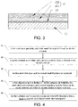
- Fig. 1 shows Embodiment 1 of the present disclosure, which provides a liquid crystal antenna.
- the liquid crystal antenna includes a first substrate 11 and a second substrate 21 which are oppositely arranged, and further includes a liquid crystal layer 30 positioned between the first substrate 11 and the second substrate 21.
- sealant 40 between the first substrate 11 and the second substrate 21.
- the sealant 40 is located at the edges of the first substrate 11 and the second substrate 21, and is used for sealing the liquid crystal layer 30.
- supports are distributed in the liquid crystal layer 30.
- the first substrate 11 and the second substrate 21 are made of materials with good effect on stability and insulation and extremely low dielectric loss.
- the first substrate 11 and the second substrate 21 are rigid substrates, which can be made of a glass material, molten quartz, a ceramic material or a ceramic thermosetting polymer composite, but is preferably a glass substrate.
- the first substrate 11 is provided with a first conductive layer and the second substrate 21 is provided with a second conductive layer.
- the first conductive layer includes a first metal film layer 13 disposed on one side, facing the second substrate 21, of the first substrate 11, and the second conductive layer includes a second metal film layer 22 disposed on one side, facing the first substrate 11, of the second substrate 21.
- At least one of the first metal film layer 13 and the second metal film layer 22 is a patterned metal film layer.
- the metal materials of the first metal film layer 13 and the second metal film layer 22 have high conductivity and magnetic permeability, which may be aluminum, copper, silver, gold, cadmium, chromium, molybdenum, niobium, nickel and iron, preferably silver, copper, gold, aluminum and alloys thereof.
- the skin effect indirectly increases the resistance of a conductor, and the energy and heat loss also increases. In high-frequency bands such as microwave, the skin effect is very obvious. Different metal materials have different skin depths.
- Skin effect when there is an alternating current or alternating electromagnetic field in the conductor, the current distribution inside the conductor is not uniform, and the current is concentrated on the outer skin part of the conductor; and the closer to the surface of the conductor, the greater the current density is, and the actual current inside the conductor is very small. As a result, the resistance of the conductor increases and the loss power of the conductor also increases. This phenomenon is called skin effect.
- ⁇ represents the magnetic permeability of the metal material
- ⁇ represents the conductivity of the conductor
- f represents the frequency of a signal carried by the liquid crystal antenna.
- the skin effect required by the liquid crystal antenna generally requires the thicknesses of the corresponding first metal film layer 13 and second metal film layer 22 to be between 3 times and 5 times the skin depth ⁇ respectively.
- the thickness of each metal film layer must reach the ⁇ m grade to ensure the performance of the liquid crystal antenna.
- silver has the best conductivity but is expensive, and is generally suitable for vacuum magnetron sputtering process.
- Gold is more expensive and is not suitable for subtractive etching of patterns and wirings.
- Aluminum is generally suitable for vacuum magnetron sputtering process.
- the metal materials of the metal film layers are preferably copper.
- the materials of the first metal film layer 13 and the second metal film layer 22 are both copper, and the thicknesses of the first metal film layer 13 and the second metal film layer 22 are of the ⁇ m grade, which can ensure the performance of the liquid crystal antenna.
- the thicknesses of the first metal film layer 13 and the second metal film layer 22 are not less than 2.0 ⁇ m.
- metal film plating processes carried out on glass substrates adopt vacuum magnetron sputtering (PVD), chemical vapor deposition (CVD) and sublimation evaporation as mature large-scale manufacturing methods in existing liquid crystal panels.
- the materials of the metal film layers are silver, copper, gold, aluminum and alloys thereof.
- Chemical vapor deposition (CVD) used in the manufacture of liquid crystal panels is not suitable for the manufacture of pure metal film layers, but is suitable for the manufacture of materials such as III-V, II-IV, IV-VI binary or polynary compounds, oxides, sulfides, nitrides, carbides, and hydrides.
- Sublimation evaporation is suitable for OLED luminescent materials, and the pure silver evaporation process is suitable for in a solution where the entire surface of a cathode is not etched, but is not suitable for making products with wires or patterns due to its high tendency to oxidization. In addition, the high cost of an entire thick film is also a problem.
- the metal film layers are plated on the glass substrates by the chemical deposition method, which can avoid the problems of repeated plating, low efficiency, serious thermal deformation and the like in the vacuum magnetron sputtering process.
- the chemical deposition method herein is different from chemical vapor deposition (CVD).
- Chemical vapor deposition (CVD) is dry deposition, while chemical deposition is carried out in a solution and is an oxidation-reduction reaction.
- the chemical deposition method may also be referred to as a chemical copper deposition method.
- the metal film layers can be formed on the substrates through chemical deposition method.
- the chemical copper deposition method and the electroplating method in the prior art are not suitable for directly plating a metal film layer, such as a copper layer, on the smooth glass substrate, or even if the metal film layer is plated, the adhesion between the metal film layer and the glass substrate is extremely poor, and the serious problem which is the metal film layer tends to fall off the smooth glass surface would be caused.
- the first metal film layer 13 is formed by plating a film on the first substrate 11 through the chemical deposition process.
- a seed layer 24 is formed on the surface of the substrate first, which can greatly improve the adhesion between the metal film layer and the glass.
- the seed layer 24 is a metal oxide film, and the metal oxide is, for example, tin oxide, nickel oxide, titanium oxide, copper oxide or a mixture thereof.
- the thickness of the seed layer 24 affects the performance and loss of the antenna, so the seed layer 24 is generally thin, for example, less than 50 nm thick.
- the seed layer 24 has a thickness of less than 20 nm.
- a chemically deposited layer 131 is plated on the surface of the seed layer 24 by the chemical deposition method.
- the chemically deposited layer 131 can be obtained.
- the materials of the metal film layers are copper
- the chemical deposition method is a chemical copper deposition method.
- the chemically deposited layer 131 is a deposited copper layer.
- the metal film layers can be obtained by chemical deposition method.
- the first metal film layer 13 is a chemically deposited layer 131 laminated on the seed layer 24 of the corresponding first substrate 11.
- the second metal film layer 22 is a chemically deposited layer 131 laminated on the seed layer 24 of the corresponding second substrate 21.
- the thickness of the chemically deposited layer 131 and an electroplated metal layer 132 of the first metal film layer 13 is 2.0 ⁇ m or more.
- the thickness of the chemically deposited layer 131 and an electroplated metal layer 132 of the second metal film layer 22 is 2.0 ⁇ m or more.
- the surface of the metal film layer is rough, and the porosity of the film layer is high, which means that atoms are not closely arranged. These all affect the performance of the antenna. Besides, the plating efficiency is lower than that of electrocoppering.
- the conductive layers of the metal film layers After the conductive layers of the metal film layers are formed through plating, the conductive layers can be patterned according to the actual situation to obtain patterned metal film layers.
- the second conductive layer and the first conductive layer are both patterned metal film layers.
- the first conductive layer is a planar electrode, such as a planar grounding electrode, so that the patterning step can be omitted for the first conductive layer
- the second conductive layer is a patterned metal film layer, such as a phase shifter electrode.
- the liquid crystal antenna further includes a first alignment layer 14 and a second alignment layer 23 disposed on the two sides of the liquid crystal layer 30 respectively.
- the first alignment layer 14 is prepared on the first substrate 11 on which the first conductive layer is formed
- the second alignment layer 23 is prepared on the second substrate 21 on which the second conductive layer is formed.
- the alignment layers are used to define the initial deflection angle of crystal molecules of the liquid crystal layer 30.
- the first substrate 11, the second substrate 21, the liquid crystal layer 30, a first conductive layer, and a second conductive layer constitute a liquid crystal phase shifter.
- the liquid crystal antenna further includes an antenna radiation unit.
- the antenna radiation unit is used for radiating microwave signals to realize the feed-in and feed-out of microwave signals.
- the antenna radiation unit is disposed on one side, away from the second substrate 21, of the first substrate 11.
- the antenna radiation unit is made of a highly conductive material.
- the antenna radiation unit can be a rectangular, circular or square patch, and can be chamfered, or can be attached to a liquid crystal phase shifter through SMT.
- the antenna radiation unit is a patterned third metal film layer 12 disposed on one side, away from the second substrate 21, of the first substrate 11. The thickness of the third metal film layer 12 do not need to reach the thicknesses of the first metal film layer 13 and the second metal film layer 22.
- the second conductive layer includes a phase shifter electrode, which is a planar transmission line for transmitting microwave signals.
- the planar transmission line is preferably a microstrip line.
- the shape of the microstrip line can be serpentine or spiral, which is not limited, as along as the transmission of the microwave signals can be realized.
- the first conductive layer includes a grounding electrode.
- the first conductive layer that is, the first metal film layer 13, is also provided with a slit unit 15.
- the slit unit 15 is a groove formed in the first metal film layer 13 and is located below the antenna radiation unit.
- the slot unit 15 is used to couple RF signals between the antenna radiation unit and the phase shifter.
- the liquid crystal antenna also includes an offset line.
- the offset line may be disposed on the second metal film layer of the second substrate.
- the liquid crystal molecules are arranged in a preset direction under the action of the first alignment layer and the second alignment layer.
- the electric field drives deflection of the direction of the liquid crystal molecules in the liquid crystal layer 30.
- the microwave signals are transmitted between the microstrip line and the grounding electrode. During the transmission of the microwave signals, the phase will be changed due to the deflection of the liquid crystal molecules, thus realizing the phase shift function of the microwave signals.
- the deflection angle of liquid crystal in the liquid crystal layer 30 can be controlled, and further the phase adjusted in the phase shifting process can be controlled.
- the effective dielectric constant of the liquid crystal is changed by controlling the voltage applied to the liquid crystal layer 30 based on the dielectric anisotropy characteristic and the low power consumption characteristic of the liquid crystal material, thereby controlling the phase adjusted in the phase shifting process.
- Two-dimensional patterns are formed by specially designed liquid crystal antenna units with different electrostatic capacitances. Electromagnetic waves received or emitted from the antenna are given with phase differences corresponding to the electrostatic capacitances of each antenna unit, and the two-dimensional patterns formed by the antenna units with different electrostatic capacitances have strong directivity (beam scanning) in a specific direction, thus realizing the function of mutual conversion between electromagnetic waves received or emitted by the antenna and radio frequency signals (voltage signals).
- the seed layers 24 are firstly manufactured on the surfaces of the substrates, and then the corresponding metal film layers are formed on the seed layers 24 through plating, so that the thicknesses of the metal film layers can reach the ⁇ m grade, and the performance of the liquid crystal antenna is ensured.
- the problems of repeated plating, low efficiency, serious thermal deformation and the like in the vacuum magnetron sputtering process are avoided, the adhesion between the metal film layers and the substrates is strong, and a liquid crystal antenna which can be manufactured on a large scale at low cost is provided.
- the present embodiment is different from Embodiment 1 in that, the chemically deposited layers 131 are first fabricated on the seed layers 24 of the corresponding substrates, and then the electroplated metal layers 132 are fabricated on the chemically deposited layers 131 by an electroplating process. That is, the metal film layers are plated on the substrates by oppositely bonding chemical deposition with electroplating.
- the electroplating process is different from the chemical deposition method in that electroplating is an electrolytic reaction which requires power to be applied to a substrate carrier; however, chemical deposition method, such as chemical copper deposition method, is an oxidation-reduction reaction which does not require power on the substrate carrier.
- the first metal film layer 13 and the second metal film layer 22 are each composed of the seed layer 24, the chemically deposited layer 131, and the electroplated metal layer 132 which are sequentially laminated on the corresponding substrate.
- the chemically deposited layers 131 serve as a conductive part.
- the thicknesses of the chemically deposited layers 131 are smaller than the thicknesses of the electroplated metal layers 132.
- the metal materials of the chemically deposited layers 131 and the electroplated metal layers 132 are the same.
- the metal materials of the metal film layers are preferably copper, the chemically deposited layers 131 are deposited copper layers, and the electroplated metal layers 132 are also copper layers.
- the thicknesses of the chemically deposited layers 131 are 0.1 ⁇ m-1.0 ⁇ m, and the thicknesses of the electroplated metal layers 132 are 2.0 ⁇ m or more.
- the electroplating method Compared with the chemical deposition method, the electroplating method has the advantages that the surface of the obtained metal film layer is smooth, and internal metal atoms are closely arranged, so that the antenna has better performance.
- the efficiency of electroplating is greatly improved compared with the forming efficiency of the chemically deposited layers 131.
- This specific embodiment provides a method for manufacturing the liquid crystal antenna as in Embodiment 2.
- the method for manufacturing the liquid crystal antenna includes the following steps:
- a method for plating the seed layers 24 includes the following step: chemically deposited layers 131 are plated on the surfaces of the seed layers 24 by a chemical deposition method.
- the chemical deposition method is a chemical copper deposition method, deposited copper layers are formed by plating the seed layers 24.
- step S1 and step S2 can be adjusted.
- step S3 When the metal film layers are patterned in step S3, if one of the conductive layers is a planar electrode, the patterning step can be omitted.
- the method for manufacturing the liquid crystal antenna further includes the following step: S4: a first alignment layer 14 is formed on the first substrate 11 on which the first conductive layer is formed, and a second alignment layer 23 is formed on the second substrate 21 on which the second conductive layer is formed.
- the method for manufacturing the liquid crystal antenna further includes the following step: S5: the first substrate 11 and the second substrate 21 are oppositely bonded to form a liquid crystal cell, and a liquid crystal layer 30 is prepared.
- the first substrate 11 and the second substrate 21 may be first oppositely bonded to form the liquid crystal cell, which is then filled with the liquid crystal layer 30. It is known that before the first substrate 11 and the second substrate 21 are oppositely bonded, sealant 40 is also prepared on one of the substrates, and the sealant 40 forms an accommodation space between the first substrate 11 and the second substrate 21 for receiving liquid crystal. After the liquid crystal cell is filled with the liquid crystal layer 30, the liquid crystal cell is sealed and the sealant 40 is cured.
- the order of oppositely bonding to form the liquid crystal cell and preparing the liquid crystal layer 30 is not limited to the above, but may also be: after one of the substrates is coated with the sealant 40, liquid crystal is dripped on the substrate to form the liquid crystal layer 30, the first substrate 11 and the second substrate 21 are oppositely bonded to form the liquid crystal cell, and then the sealant 40 is cured.
- the first metal film layer 13 can be patterned as follows: the first metal film layer 13 is coated with a layer of photoresist; the photoresist is exposed by using a mask plate to form a photoresist non-retained area and a photoresist retained area, wherein the photoresist retained area corresponds to the area where a pattern of the first conductive layer is located, and the photoresist non-retained area corresponds to the area other than the above pattern; development is conducted, wherein the photoresist in the photoresist non-retained area is completely removed, and the thickness of the photoresist in the photoresist retained area remains unchanged; the conductive layer in the photoresist non-retained area is completely etched away through etching; and the remaining photoresist is stripped to form the pattern of the first conductive layer.
- the alignment layers can be made by PI friction process in the prior art so as to form orientational grooves on the surfaces, which will not be detailed here.
- a method for plating the substrates with the metal film layers mainly involves the process of the combination of chemical deposition method and electroplating, and includes the following steps:
- step (a) above is an optional step
- step (c) above is a more optimized solution, that is, plating can still be carried out without step (c), but the effect is slightly poor.
- the immersion pulling manufacturing process of the seed layers 24 includes the following steps: a solution with a metal oxide as the main component is prepared, the substrates are immersed into the prepared metal oxide solution by the immersion pulling method, the substrates are pulled out of the solution to attach the metal oxide to the substrates, and then drying treatment is performed, such as natural air drying or drying at a certain temperature, to obtain metal oxide films on the substrates.
- the thicknesses of the seed layers 24 affect the performance and loss of the antenna, so the thicknesses of the seed layers 24 are generally small, for example, less than 50 nm.
- the immersion pulling process is adopted to generate the seed layers 24 on the substrate surfaces. Through the immersion pulling process, uniform thin film layers can be plated on the smooth substrate surfaces. Other processes, such as vacuum magnetron sputtering, are not suitable for making the seed layers 24 because the surface of a film prepared thereby is too smooth.
- the above method for plating the glass substrates mainly adopts the electroplating process.
- the problem that a metal film layer such as a copper layer cannot be directly plated on a smooth glass substrate by the electroplating process in the prior art is solved.
- the adhesion between the metal film layers and the glass substrates is strong.
- the method does not require repeated plating, can produce a film layer with a thickness of the ⁇ m grade, has high efficiency and yield, reduces the cost of the final liquid crystal antenna, and can realize large-scale manufacture.
- the first conductive layer and the second conductive layer with ⁇ m-grade thicknesses can be produced on a large scale at low cost.
- the liquid crystal antenna can be produced in large quantities.
- the above method for plating the glass substrates further includes performing a first baking treatment after the seed layers 24 are generated in step (b) and before the seed layers 24 are activated in step (c).
- the function of the first baking treatment is to enhance the adhesion to glass through through high-temperature baking.
- step (d) chemical liquid on the surfaces of the chemically deposited layers 131 is cleaned to prevent residual chemical liquid from polluting the surfaces of the chemically deposited layers 131.
- step (e) chemical liquid on the surfaces of the chemically deposited layers 131 is cleaned to prevent residual chemical liquid from polluting the surfaces of the chemically deposited layers 131.
- a second baking treatment is performed.
- the function of the second baking treatment is to release the stress accumulated in the process of making the chemically deposited layers 131 and enhance the metal compactness and adhesion of the chemically deposited layers 131 through high-temperature baking.
- Process of the electroplating or the chemically deposited layer 131 uses the principles of electrochemical reactions to transfer metal ions to the surface of the substrate through the current effect and stack the metal ions. As it is difficult to accurately stack metal atoms, the result of the process is that the porosity of the metal film layer is high, and the atoms are not closely arranged. Through baking, the metal atoms are stacked and arranged again under thermal stress at a high temperature, so that the metal atoms are closer, the attraction force between the atoms is greater, and the metal compactness and adhesion of the chemically deposited layers 131 are enhanced.
- step (e) cleaning is performed to remove the chemical liquid on the electroplated metal layers 132 to prevent residual chemical liquid from polluting the electroplated metal layers 132, and then third baking treatment is carried out.
- the function of the third baking treatment is similar to that of the second baking treatment above through through high-temperature baking.
- baking treatment is conducted several times at different stages, so that the stress accumulated in the previous film layer manufacturing process is released in time, the adhesion between the corresponding film layer and the glass substrate is enhanced, the adhesion can be as high as that of the vacuum magnetron sputtering plating technology, and the technical index is that the adhesion tested by a cross-cut tester is more than 5B. After the adhesion is satisfactory, the liquid crystal antenna can be produced in large quantities in an existing liquid crystal panel production line.
- the denser metal film layers reduce the loss of the liquid crystal antenna.
- An antenna radiation unit can be attached to one side, away from the second substrate 21, of the first substrate 11 through SMT.
- the antenna radiation unit may be obtained by forming a metal film layer on the surface of the first substrate 11 and then treating the metal film layer.
- the antenna radiation unit is a patterned third metal film layer 12 arranged on one side, away from the second substrate 21, of the first substrate 11.
- the method for manufacturing the liquid crystal antenna further includes the following steps: a third metal film layer 12 is formed on one side, away from the second substrate 21, of the first substrate 11 by plating, and the third metal film layer 12 is patterned to obtain an antenna radiation unit.
- the forming of the third metal film layer 12 on the first substrate 11 may be performed before forming the first metal film layer 13 or after forming the first metal film layer 13, which is not limited herein.
- the patterning of the third metal film layer 12 may be performed after patterning the first metal film layer 13, but is not limited thereto. The specific operation can be carried out with reference to the above-mentioned method for plating the glass substrate and the patterning process.
- each metal film layer includes only the chemically deposited layer 131 laminated on the seed layer 24 of the corresponding substrate, and does not include the electroplated metal layer 132.
- a method for plating the substrates with the metal film layers mainly involves the process of chemical deposition method, and includes the following steps:
- step (e) is omitted.
- step (d) chemical liquid on the surfaces of the chemically deposited layers 131 is cleaned to prevent residual chemical liquid from polluting the surfaces of the chemically deposited layers 131.
- a second baking treatment is performed after cleaning the chemically deposited layers 131.
- the function of the second baking treatment is to release the stress accumulated in the process of making the chemically deposited layers 131 and enhance the metal compactness and adhesion of the chemically deposited layers 131 through high-temperature baking.
- the metal atoms are stacked and arranged again under thermal stress at a high temperature, so that the metal atoms are closer, the attraction force between the atoms is greater, and the metal compactness and adhesion of the chemically deposited layers 131 are enhanced.
- the disclosure has the following beneficial effects:
- a metal film layer such as a copper layer cannot be directly plated on a smooth glass substrate by the electroplating process in the prior art is solved.
- the adhesion between the metal film layers and the substrates is strong.
- the method does not require repeated plating, can efficiently produce a film layer with a thickness of the ⁇ m grade, is suitable for large-scale manufacture, and reduces the cost of the final liquid crystal antenna.
- the first conductive layer and the second conductive layer with ⁇ m-grade thicknesses can be produced on a large scale at low cost.
- the liquid crystal antenna can be produced in large quantities.
Landscapes
- Physics & Mathematics (AREA)
- Nonlinear Science (AREA)
- Optics & Photonics (AREA)
- Crystallography & Structural Chemistry (AREA)
- Chemical & Material Sciences (AREA)
- General Physics & Mathematics (AREA)
- Mathematical Physics (AREA)
- Chemically Coating (AREA)
- Details Of Aerials (AREA)
- Liquid Crystal (AREA)
- Waveguide Switches, Polarizers, And Phase Shifters (AREA)
- Variable-Direction Aerials And Aerial Arrays (AREA)
- Waveguide Aerials (AREA)
- Physical Vapour Deposition (AREA)
Applications Claiming Priority (2)
| Application Number | Priority Date | Filing Date | Title |
|---|---|---|---|
| CN201910185803.1A CN109818150A (zh) | 2019-03-12 | 2019-03-12 | 一种液晶天线及其制作方法 |
| PCT/CN2019/078174 WO2020181558A1 (fr) | 2019-03-12 | 2019-03-14 | Antenne à cristaux liquides et son procédé de fabrication |
Publications (3)
| Publication Number | Publication Date |
|---|---|
| EP3736626A1 true EP3736626A1 (fr) | 2020-11-11 |
| EP3736626A4 EP3736626A4 (fr) | 2020-11-11 |
| EP3736626B1 EP3736626B1 (fr) | 2023-09-06 |
Family
ID=66608794
Family Applications (1)
| Application Number | Title | Priority Date | Filing Date |
|---|---|---|---|
| EP19863991.6A Active EP3736626B1 (fr) | 2019-03-12 | 2019-03-14 | Antenne à cristaux liquides et son procédé de fabrication |
Country Status (7)
| Country | Link |
|---|---|
| US (1) | US11156859B2 (fr) |
| EP (1) | EP3736626B1 (fr) |
| JP (1) | JP6992185B2 (fr) |
| KR (1) | KR102326746B1 (fr) |
| CN (1) | CN109818150A (fr) |
| TW (1) | TWI721822B (fr) |
| WO (1) | WO2020181558A1 (fr) |
Cited By (1)
| Publication number | Priority date | Publication date | Assignee | Title |
|---|---|---|---|---|
| TWI788156B (zh) * | 2021-09-07 | 2022-12-21 | 稜研科技股份有限公司 | 電磁波傳輸結構 |
Families Citing this family (26)
| Publication number | Priority date | Publication date | Assignee | Title |
|---|---|---|---|---|
| RS63712B1 (sr) | 2018-07-10 | 2022-11-30 | Glaxosmithkline Ip Dev Ltd | Jedinjenja c-manozida korisna za tretman infekcija urinarnog trakta |
| CA3138394A1 (fr) | 2019-05-07 | 2020-11-12 | Glaxosmithkline Intellectual Property Development Limited | Nouveaux composes |
| CN112018518B (zh) * | 2019-05-29 | 2025-05-16 | 富泰华工业(深圳)有限公司 | 天线阵列及具有所述天线阵列的液晶显示器 |
| CN111430894B (zh) * | 2020-04-01 | 2021-08-03 | 电子科技大学 | 一种共形液晶光学相控阵的光学装置 |
| US20210313705A1 (en) * | 2020-04-03 | 2021-10-07 | Kymeta Corporation | Rf element design for improved tuning range |
| CN111525264B (zh) * | 2020-05-21 | 2022-01-18 | 信利(仁寿)高端显示科技有限公司 | 一种液晶天线 |
| CN113871818B (zh) * | 2020-06-30 | 2022-07-26 | 上海天马微电子有限公司 | 移相器及其制作方法、天线及其制作方法 |
| CN114388996B (zh) * | 2020-10-22 | 2023-04-07 | 上海天马微电子有限公司 | 液晶移相器及其制作方法、液晶天线 |
| CN112688037B (zh) * | 2020-12-31 | 2022-05-20 | 成都天马微电子有限公司 | 一种液晶移相器及其制备方法、液晶天线 |
| CN112909560B (zh) * | 2021-01-15 | 2022-08-02 | 成都天马微电子有限公司 | 液晶天线及其制作方法 |
| CN114914695B (zh) * | 2021-02-07 | 2024-06-25 | 上海天马微电子有限公司 | 一种天线基板及天线 |
| CN112904623A (zh) * | 2021-02-23 | 2021-06-04 | 南京华日触控显示科技有限公司 | 利用四次光刻工艺制作四层铜结构液晶盒及其制备方法 |
| TWI754559B (zh) * | 2021-03-08 | 2022-02-01 | 友達光電股份有限公司 | 相位調制單元以及輻射系統 |
| US11990680B2 (en) * | 2021-03-18 | 2024-05-21 | Seoul National University R&Db Foundation | Array antenna system capable of beam steering and impedance control using active radiation layer |
| CN115117609B (zh) | 2021-03-23 | 2024-07-05 | 京东方科技集团股份有限公司 | 天线单元及其制备方法、电子设备 |
| JP7593862B2 (ja) * | 2021-03-31 | 2024-12-03 | 日東電工株式会社 | アンテナフィルム |
| WO2022259896A1 (fr) * | 2021-06-08 | 2022-12-15 | Agc株式会社 | Substrat pour dispositif haute fréquence |
| CN113905518A (zh) * | 2021-09-10 | 2022-01-07 | 北京华镁钛科技有限公司 | 一种液晶天线面板及其制造工艺 |
| CN118285023A (zh) * | 2021-11-25 | 2024-07-02 | 株式会社日本显示器 | 电波反射板 |
| WO2023108626A1 (fr) * | 2021-12-17 | 2023-06-22 | 京东方科技集团股份有限公司 | Antenne réseau à commande de phase, procédé de balayage associé et système d'antenne |
| CN114284714B (zh) * | 2021-12-31 | 2023-12-15 | 成都天马微电子有限公司 | 液晶天线及其制备方法 |
| JPWO2024029170A1 (fr) * | 2022-08-01 | 2024-02-08 | ||
| WO2024040616A1 (fr) * | 2022-08-26 | 2024-02-29 | 京东方科技集团股份有限公司 | Déphaseur réglable et procédé de fabrication correspondant, et dispositif électronique |
| CN115693130A (zh) * | 2022-11-11 | 2023-02-03 | 成都天马微电子有限公司 | 天线及通信设备 |
| KR20250046145A (ko) | 2023-09-26 | 2025-04-02 | 대한민국(방위사업청장) | 저전압 구동을 위한 액정 기반 주파수 가변 안테나의 제조방법 |
| TWI881851B (zh) * | 2024-06-04 | 2025-04-21 | 友達光電股份有限公司 | 天線裝置 |
Family Cites Families (15)
| Publication number | Priority date | Publication date | Assignee | Title |
|---|---|---|---|---|
| JPH02162804A (ja) * | 1988-12-16 | 1990-06-22 | Nissan Motor Co Ltd | 平板型アンテナ |
| TW344034B (en) * | 1996-12-06 | 1998-11-01 | Nat Science Council | Process for fabricating an optical filter polarizer |
| JP2008297168A (ja) | 2007-05-31 | 2008-12-11 | National Institute Of Advanced Industrial & Technology | ZnOウィスカー膜及びその作製方法 |
| JP5518355B2 (ja) | 2009-03-26 | 2014-06-11 | 公益財団法人神奈川科学技術アカデミー | 導電体基板、導電体基板の製造方法、デバイス及び電子機器 |
| CN102463130A (zh) | 2010-11-19 | 2012-05-23 | 北京佳盛世纪科技有限公司 | 一种溶胶-凝胶法制备改性TiO2涂层的方法 |
| CN102683220B (zh) * | 2011-03-08 | 2016-01-20 | 华进半导体封装先导技术研发中心有限公司 | 一种制作多层有机液晶聚合物基板结构的方法 |
| EP2575211B1 (fr) | 2011-09-27 | 2014-11-05 | Technische Universität Darmstadt | Antenne de réseau phasée planaire orientable électroniquement |
| CN202805801U (zh) * | 2012-06-05 | 2013-03-20 | 深圳市五株科技股份有限公司 | 覆铜板和印刷电路板 |
| EP2784181B1 (fr) | 2013-03-27 | 2015-12-09 | ATOTECH Deutschland GmbH | Solution de dépôt de cuivre chimique |
| JP6589058B2 (ja) * | 2016-05-30 | 2019-10-09 | シャープ株式会社 | 走査アンテナ |
| US10720708B2 (en) * | 2016-07-25 | 2020-07-21 | Innolux Corporation | Antenna device |
| CN108321503B (zh) | 2017-01-16 | 2020-05-15 | 群创光电股份有限公司 | 液晶天线装置 |
| CN106932933B (zh) * | 2017-05-09 | 2019-08-27 | 京东方科技集团股份有限公司 | 一种液晶天线及其制作方法 |
| CN108490706B (zh) * | 2018-04-13 | 2024-04-02 | 京东方科技集团股份有限公司 | 液晶移相器及其制造方法、液晶天线及电子装置 |
| CN108963402B (zh) * | 2018-08-16 | 2023-09-26 | 北京华镁钛科技有限公司 | 一种用于制作射频微波器件及天线的传输结构及制作方法 |
-
2019
- 2019-03-12 CN CN201910185803.1A patent/CN109818150A/zh active Pending
- 2019-03-14 JP JP2020531660A patent/JP6992185B2/ja active Active
- 2019-03-14 KR KR1020207016580A patent/KR102326746B1/ko active Active
- 2019-03-14 US US16/770,083 patent/US11156859B2/en active Active
- 2019-03-14 EP EP19863991.6A patent/EP3736626B1/fr active Active
- 2019-03-14 WO PCT/CN2019/078174 patent/WO2020181558A1/fr not_active Ceased
-
2020
- 2020-03-12 TW TW109108209A patent/TWI721822B/zh not_active IP Right Cessation
Cited By (1)
| Publication number | Priority date | Publication date | Assignee | Title |
|---|---|---|---|---|
| TWI788156B (zh) * | 2021-09-07 | 2022-12-21 | 稜研科技股份有限公司 | 電磁波傳輸結構 |
Also Published As
| Publication number | Publication date |
|---|---|
| TWI721822B (zh) | 2021-03-11 |
| JP6992185B2 (ja) | 2022-01-13 |
| KR20200110305A (ko) | 2020-09-23 |
| US11156859B2 (en) | 2021-10-26 |
| WO2020181558A1 (fr) | 2020-09-17 |
| US20210208430A1 (en) | 2021-07-08 |
| KR102326746B1 (ko) | 2021-11-15 |
| CN109818150A (zh) | 2019-05-28 |
| EP3736626A4 (fr) | 2020-11-11 |
| EP3736626B1 (fr) | 2023-09-06 |
| JP2021517745A (ja) | 2021-07-26 |
| TW202103372A (zh) | 2021-01-16 |
Similar Documents
| Publication | Publication Date | Title |
|---|---|---|
| EP3736626B1 (fr) | Antenne à cristaux liquides et son procédé de fabrication | |
| CN108963402B (zh) | 一种用于制作射频微波器件及天线的传输结构及制作方法 | |
| EP3745527B1 (fr) | Déphaseur à cristaux liquides, antenne à cristaux liquides, et procédé de fabrication de déphaseur à cristaux liquides | |
| CN108493592B (zh) | 微带天线及其制备方法和电子设备 | |
| US11557837B2 (en) | Flat panel liquid crystal antenna and manufacturing method thereof | |
| CN113725597B (zh) | 液晶天线的制作方法、液晶天线 | |
| CN209786195U (zh) | 一种液晶天线 | |
| CN210720940U (zh) | 一种液晶盒、液晶天线单元和液晶相控阵天线 | |
| WO2023029908A1 (fr) | Structure de feuille de cuivre composite, son procédé de préparation, stratifié plaqué de cuivre et carte de circuit imprimé | |
| CN109950697B (zh) | 波导馈电基板及其制备方法、天线系统及其制备方法 | |
| JP2020501460A (ja) | 低損失電送機構及びそれを使用するアンテナ | |
| CN209544616U (zh) | 一种平板液晶天线 | |
| WO2018097017A1 (fr) | Ligne de transmission | |
| Teshirogi et al. | High-efficiency, dielectric slab leaky-wave antennas | |
| CN113991305A (zh) | 一种新型异质基板液晶相控天线以及制造方法 | |
| WO2021174422A1 (fr) | Antenne transparente et son procédé de fabrication et dispositif électronique | |
| Wang et al. | Research on Transmission Line based on Fused Quartz with TGV Structure | |
| US20230070751A1 (en) | Integral 5g antenna structure | |
| Faliero et al. | A Wideband Glass Resonator Antenna as AiP Concept for Sub-THz Application | |
| CN120657426A (zh) | 天线装置 | |
| CN118073827A (zh) | 一种透明天线制作方法及透明天线 | |
| CN118117327A (zh) | 一种基于人工导体的低损耗微带天线及其制备方法 | |
| Zhang et al. | Design of printed monopole antennas on liquid crystal polymer substrates |
Legal Events
| Date | Code | Title | Description |
|---|---|---|---|
| STAA | Information on the status of an ep patent application or granted ep patent |
Free format text: STATUS: UNKNOWN |
|
| STAA | Information on the status of an ep patent application or granted ep patent |
Free format text: STATUS: THE INTERNATIONAL PUBLICATION HAS BEEN MADE |
|
| PUAI | Public reference made under article 153(3) epc to a published international application that has entered the european phase |
Free format text: ORIGINAL CODE: 0009012 |
|
| STAA | Information on the status of an ep patent application or granted ep patent |
Free format text: STATUS: REQUEST FOR EXAMINATION WAS MADE |
|
| 17P | Request for examination filed |
Effective date: 20200403 |
|
| A4 | Supplementary search report drawn up and despatched |
Effective date: 20201013 |
|
| AK | Designated contracting states |
Kind code of ref document: A1 Designated state(s): AL AT BE BG CH CY CZ DE DK EE ES FI FR GB GR HR HU IE IS IT LI LT LU LV MC MK MT NL NO PL PT RO RS SE SI SK SM TR |
|
| AX | Request for extension of the european patent |
Extension state: BA ME |
|
| STAA | Information on the status of an ep patent application or granted ep patent |
Free format text: STATUS: EXAMINATION IS IN PROGRESS |
|
| 17Q | First examination report despatched |
Effective date: 20220118 |
|
| DAV | Request for validation of the european patent (deleted) | ||
| DAX | Request for extension of the european patent (deleted) | ||
| GRAP | Despatch of communication of intention to grant a patent |
Free format text: ORIGINAL CODE: EPIDOSNIGR1 |
|
| STAA | Information on the status of an ep patent application or granted ep patent |
Free format text: STATUS: GRANT OF PATENT IS INTENDED |
|
| INTG | Intention to grant announced |
Effective date: 20230515 |
|
| GRAS | Grant fee paid |
Free format text: ORIGINAL CODE: EPIDOSNIGR3 |
|
| GRAA | (expected) grant |
Free format text: ORIGINAL CODE: 0009210 |
|
| STAA | Information on the status of an ep patent application or granted ep patent |
Free format text: STATUS: THE PATENT HAS BEEN GRANTED |
|
| AK | Designated contracting states |
Kind code of ref document: B1 Designated state(s): AL AT BE BG CH CY CZ DE DK EE ES FI FR GB GR HR HU IE IS IT LI LT LU LV MC MK MT NL NO PL PT RO RS SE SI SK SM TR |
|
| REG | Reference to a national code |
Ref country code: GB Ref legal event code: FG4D |
|
| REG | Reference to a national code |
Ref country code: CH Ref legal event code: EP |
|
| REG | Reference to a national code |
Ref country code: IE Ref legal event code: FG4D |
|
| REG | Reference to a national code |
Ref country code: DE Ref legal event code: R096 Ref document number: 602019037090 Country of ref document: DE |
|
| REG | Reference to a national code |
Ref country code: LT Ref legal event code: MG9D |
|
| REG | Reference to a national code |
Ref country code: NL Ref legal event code: MP Effective date: 20230906 |
|
| PG25 | Lapsed in a contracting state [announced via postgrant information from national office to epo] |
Ref country code: GR Free format text: LAPSE BECAUSE OF FAILURE TO SUBMIT A TRANSLATION OF THE DESCRIPTION OR TO PAY THE FEE WITHIN THE PRESCRIBED TIME-LIMIT Effective date: 20231207 |
|
| PG25 | Lapsed in a contracting state [announced via postgrant information from national office to epo] |
Ref country code: SE Free format text: LAPSE BECAUSE OF FAILURE TO SUBMIT A TRANSLATION OF THE DESCRIPTION OR TO PAY THE FEE WITHIN THE PRESCRIBED TIME-LIMIT Effective date: 20230906 Ref country code: RS Free format text: LAPSE BECAUSE OF FAILURE TO SUBMIT A TRANSLATION OF THE DESCRIPTION OR TO PAY THE FEE WITHIN THE PRESCRIBED TIME-LIMIT Effective date: 20230906 Ref country code: NO Free format text: LAPSE BECAUSE OF FAILURE TO SUBMIT A TRANSLATION OF THE DESCRIPTION OR TO PAY THE FEE WITHIN THE PRESCRIBED TIME-LIMIT Effective date: 20231206 Ref country code: LV Free format text: LAPSE BECAUSE OF FAILURE TO SUBMIT A TRANSLATION OF THE DESCRIPTION OR TO PAY THE FEE WITHIN THE PRESCRIBED TIME-LIMIT Effective date: 20230906 Ref country code: LT Free format text: LAPSE BECAUSE OF FAILURE TO SUBMIT A TRANSLATION OF THE DESCRIPTION OR TO PAY THE FEE WITHIN THE PRESCRIBED TIME-LIMIT Effective date: 20230906 Ref country code: HR Free format text: LAPSE BECAUSE OF FAILURE TO SUBMIT A TRANSLATION OF THE DESCRIPTION OR TO PAY THE FEE WITHIN THE PRESCRIBED TIME-LIMIT Effective date: 20230906 Ref country code: GR Free format text: LAPSE BECAUSE OF FAILURE TO SUBMIT A TRANSLATION OF THE DESCRIPTION OR TO PAY THE FEE WITHIN THE PRESCRIBED TIME-LIMIT Effective date: 20231207 Ref country code: FI Free format text: LAPSE BECAUSE OF FAILURE TO SUBMIT A TRANSLATION OF THE DESCRIPTION OR TO PAY THE FEE WITHIN THE PRESCRIBED TIME-LIMIT Effective date: 20230906 |
|
| REG | Reference to a national code |
Ref country code: AT Ref legal event code: MK05 Ref document number: 1609296 Country of ref document: AT Kind code of ref document: T Effective date: 20230906 |
|
| PG25 | Lapsed in a contracting state [announced via postgrant information from national office to epo] |
Ref country code: NL Free format text: LAPSE BECAUSE OF FAILURE TO SUBMIT A TRANSLATION OF THE DESCRIPTION OR TO PAY THE FEE WITHIN THE PRESCRIBED TIME-LIMIT Effective date: 20230906 |
|
| PG25 | Lapsed in a contracting state [announced via postgrant information from national office to epo] |
Ref country code: IS Free format text: LAPSE BECAUSE OF FAILURE TO SUBMIT A TRANSLATION OF THE DESCRIPTION OR TO PAY THE FEE WITHIN THE PRESCRIBED TIME-LIMIT Effective date: 20240106 |
|
| PG25 | Lapsed in a contracting state [announced via postgrant information from national office to epo] |
Ref country code: AT Free format text: LAPSE BECAUSE OF FAILURE TO SUBMIT A TRANSLATION OF THE DESCRIPTION OR TO PAY THE FEE WITHIN THE PRESCRIBED TIME-LIMIT Effective date: 20230906 |
|
| PG25 | Lapsed in a contracting state [announced via postgrant information from national office to epo] |
Ref country code: ES Free format text: LAPSE BECAUSE OF FAILURE TO SUBMIT A TRANSLATION OF THE DESCRIPTION OR TO PAY THE FEE WITHIN THE PRESCRIBED TIME-LIMIT Effective date: 20230906 |
|
| PG25 | Lapsed in a contracting state [announced via postgrant information from national office to epo] |
Ref country code: SM Free format text: LAPSE BECAUSE OF FAILURE TO SUBMIT A TRANSLATION OF THE DESCRIPTION OR TO PAY THE FEE WITHIN THE PRESCRIBED TIME-LIMIT Effective date: 20230906 Ref country code: RO Free format text: LAPSE BECAUSE OF FAILURE TO SUBMIT A TRANSLATION OF THE DESCRIPTION OR TO PAY THE FEE WITHIN THE PRESCRIBED TIME-LIMIT Effective date: 20230906 Ref country code: IS Free format text: LAPSE BECAUSE OF FAILURE TO SUBMIT A TRANSLATION OF THE DESCRIPTION OR TO PAY THE FEE WITHIN THE PRESCRIBED TIME-LIMIT Effective date: 20240106 Ref country code: ES Free format text: LAPSE BECAUSE OF FAILURE TO SUBMIT A TRANSLATION OF THE DESCRIPTION OR TO PAY THE FEE WITHIN THE PRESCRIBED TIME-LIMIT Effective date: 20230906 Ref country code: EE Free format text: LAPSE BECAUSE OF FAILURE TO SUBMIT A TRANSLATION OF THE DESCRIPTION OR TO PAY THE FEE WITHIN THE PRESCRIBED TIME-LIMIT Effective date: 20230906 Ref country code: CZ Free format text: LAPSE BECAUSE OF FAILURE TO SUBMIT A TRANSLATION OF THE DESCRIPTION OR TO PAY THE FEE WITHIN THE PRESCRIBED TIME-LIMIT Effective date: 20230906 Ref country code: AT Free format text: LAPSE BECAUSE OF FAILURE TO SUBMIT A TRANSLATION OF THE DESCRIPTION OR TO PAY THE FEE WITHIN THE PRESCRIBED TIME-LIMIT Effective date: 20230906 Ref country code: PT Free format text: LAPSE BECAUSE OF FAILURE TO SUBMIT A TRANSLATION OF THE DESCRIPTION OR TO PAY THE FEE WITHIN THE PRESCRIBED TIME-LIMIT Effective date: 20240108 Ref country code: SK Free format text: LAPSE BECAUSE OF FAILURE TO SUBMIT A TRANSLATION OF THE DESCRIPTION OR TO PAY THE FEE WITHIN THE PRESCRIBED TIME-LIMIT Effective date: 20230906 |
|
| PG25 | Lapsed in a contracting state [announced via postgrant information from national office to epo] |
Ref country code: PL Free format text: LAPSE BECAUSE OF FAILURE TO SUBMIT A TRANSLATION OF THE DESCRIPTION OR TO PAY THE FEE WITHIN THE PRESCRIBED TIME-LIMIT Effective date: 20230906 Ref country code: IT Free format text: LAPSE BECAUSE OF FAILURE TO SUBMIT A TRANSLATION OF THE DESCRIPTION OR TO PAY THE FEE WITHIN THE PRESCRIBED TIME-LIMIT Effective date: 20230906 |
|
| REG | Reference to a national code |
Ref country code: DE Ref legal event code: R097 Ref document number: 602019037090 Country of ref document: DE |
|
| PG25 | Lapsed in a contracting state [announced via postgrant information from national office to epo] |
Ref country code: DK Free format text: LAPSE BECAUSE OF FAILURE TO SUBMIT A TRANSLATION OF THE DESCRIPTION OR TO PAY THE FEE WITHIN THE PRESCRIBED TIME-LIMIT Effective date: 20230906 |
|
| PLBE | No opposition filed within time limit |
Free format text: ORIGINAL CODE: 0009261 |
|
| STAA | Information on the status of an ep patent application or granted ep patent |
Free format text: STATUS: NO OPPOSITION FILED WITHIN TIME LIMIT |
|
| PG25 | Lapsed in a contracting state [announced via postgrant information from national office to epo] |
Ref country code: DK Free format text: LAPSE BECAUSE OF FAILURE TO SUBMIT A TRANSLATION OF THE DESCRIPTION OR TO PAY THE FEE WITHIN THE PRESCRIBED TIME-LIMIT Effective date: 20230906 Ref country code: SI Free format text: LAPSE BECAUSE OF FAILURE TO SUBMIT A TRANSLATION OF THE DESCRIPTION OR TO PAY THE FEE WITHIN THE PRESCRIBED TIME-LIMIT Effective date: 20230906 |
|
| 26N | No opposition filed |
Effective date: 20240607 |
|
| REG | Reference to a national code |
Ref country code: CH Ref legal event code: PL |
|
| PG25 | Lapsed in a contracting state [announced via postgrant information from national office to epo] |
Ref country code: BG Free format text: LAPSE BECAUSE OF FAILURE TO SUBMIT A TRANSLATION OF THE DESCRIPTION OR TO PAY THE FEE WITHIN THE PRESCRIBED TIME-LIMIT Effective date: 20230906 |
|
| PG25 | Lapsed in a contracting state [announced via postgrant information from national office to epo] |
Ref country code: LU Free format text: LAPSE BECAUSE OF NON-PAYMENT OF DUE FEES Effective date: 20240314 |
|
| PG25 | Lapsed in a contracting state [announced via postgrant information from national office to epo] |
Ref country code: MC Free format text: LAPSE BECAUSE OF FAILURE TO SUBMIT A TRANSLATION OF THE DESCRIPTION OR TO PAY THE FEE WITHIN THE PRESCRIBED TIME-LIMIT Effective date: 20230906 |
|
| PG25 | Lapsed in a contracting state [announced via postgrant information from national office to epo] |
Ref country code: MC Free format text: LAPSE BECAUSE OF FAILURE TO SUBMIT A TRANSLATION OF THE DESCRIPTION OR TO PAY THE FEE WITHIN THE PRESCRIBED TIME-LIMIT Effective date: 20230906 Ref country code: LU Free format text: LAPSE BECAUSE OF NON-PAYMENT OF DUE FEES Effective date: 20240314 Ref country code: BG Free format text: LAPSE BECAUSE OF FAILURE TO SUBMIT A TRANSLATION OF THE DESCRIPTION OR TO PAY THE FEE WITHIN THE PRESCRIBED TIME-LIMIT Effective date: 20230906 |
|
| REG | Reference to a national code |
Ref country code: BE Ref legal event code: MM Effective date: 20240331 |
|
| PG25 | Lapsed in a contracting state [announced via postgrant information from national office to epo] |
Ref country code: BE Free format text: LAPSE BECAUSE OF NON-PAYMENT OF DUE FEES Effective date: 20240331 |
|
| PG25 | Lapsed in a contracting state [announced via postgrant information from national office to epo] |
Ref country code: FR Free format text: LAPSE BECAUSE OF NON-PAYMENT OF DUE FEES Effective date: 20240331 |
|
| PG25 | Lapsed in a contracting state [announced via postgrant information from national office to epo] |
Ref country code: IE Free format text: LAPSE BECAUSE OF NON-PAYMENT OF DUE FEES Effective date: 20240314 |
|
| PG25 | Lapsed in a contracting state [announced via postgrant information from national office to epo] |
Ref country code: IE Free format text: LAPSE BECAUSE OF NON-PAYMENT OF DUE FEES Effective date: 20240314 Ref country code: FR Free format text: LAPSE BECAUSE OF NON-PAYMENT OF DUE FEES Effective date: 20240331 Ref country code: BE Free format text: LAPSE BECAUSE OF NON-PAYMENT OF DUE FEES Effective date: 20240331 Ref country code: CH Free format text: LAPSE BECAUSE OF NON-PAYMENT OF DUE FEES Effective date: 20240331 |
|
| PG25 | Lapsed in a contracting state [announced via postgrant information from national office to epo] |
Ref country code: CY Free format text: LAPSE BECAUSE OF FAILURE TO SUBMIT A TRANSLATION OF THE DESCRIPTION OR TO PAY THE FEE WITHIN THE PRESCRIBED TIME-LIMIT; INVALID AB INITIO Effective date: 20190314 |
|
| PG25 | Lapsed in a contracting state [announced via postgrant information from national office to epo] |
Ref country code: HU Free format text: LAPSE BECAUSE OF FAILURE TO SUBMIT A TRANSLATION OF THE DESCRIPTION OR TO PAY THE FEE WITHIN THE PRESCRIBED TIME-LIMIT; INVALID AB INITIO Effective date: 20190314 |
|
| PG25 | Lapsed in a contracting state [announced via postgrant information from national office to epo] |
Ref country code: TR Free format text: LAPSE BECAUSE OF FAILURE TO SUBMIT A TRANSLATION OF THE DESCRIPTION OR TO PAY THE FEE WITHIN THE PRESCRIBED TIME-LIMIT Effective date: 20230906 |
|
| PGFP | Annual fee paid to national office [announced via postgrant information from national office to epo] |
Ref country code: GB Payment date: 20260302 Year of fee payment: 8 |
|
| PGFP | Annual fee paid to national office [announced via postgrant information from national office to epo] |
Ref country code: DE Payment date: 20260320 Year of fee payment: 8 |