EP3754855A1 - Détection de signal analogique via des broches d'e/s numériques - Google Patents
Détection de signal analogique via des broches d'e/s numériques Download PDFInfo
- Publication number
- EP3754855A1 EP3754855A1 EP19212838.7A EP19212838A EP3754855A1 EP 3754855 A1 EP3754855 A1 EP 3754855A1 EP 19212838 A EP19212838 A EP 19212838A EP 3754855 A1 EP3754855 A1 EP 3754855A1
- Authority
- EP
- European Patent Office
- Prior art keywords
- signal
- analog
- digital
- controller
- pulses
- Prior art date
- Legal status (The legal status is an assumption and is not a legal conclusion. Google has not performed a legal analysis and makes no representation as to the accuracy of the status listed.)
- Pending
Links
Images



Classifications
-
- H—ELECTRICITY
- H03—ELECTRONIC CIRCUITRY
- H03M—CODING; DECODING; CODE CONVERSION IN GENERAL
- H03M1/00—Analogue/digital conversion; Digital/analogue conversion
- H03M1/12—Analogue/digital converters
- H03M1/50—Analogue/digital converters with intermediate conversion to time interval
- H03M1/56—Input signal compared with linear ramp
-
- H—ELECTRICITY
- H03—ELECTRONIC CIRCUITRY
- H03F—AMPLIFIERS
- H03F3/00—Amplifiers with only discharge tubes or only semiconductor devices as amplifying elements
- H03F3/45—Differential amplifiers
-
- G—PHYSICS
- G06—COMPUTING OR CALCULATING; COUNTING
- G06F—ELECTRIC DIGITAL DATA PROCESSING
- G06F3/00—Input arrangements for transferring data to be processed into a form capable of being handled by the computer; Output arrangements for transferring data from processing unit to output unit, e.g. interface arrangements
- G06F3/01—Input arrangements or combined input and output arrangements for interaction between user and computer
- G06F3/048—Interaction techniques based on graphical user interfaces [GUI]
-
- H—ELECTRICITY
- H03—ELECTRONIC CIRCUITRY
- H03K—PULSE TECHNIQUE
- H03K7/00—Modulating pulses with a continuously-variable modulating signal
- H03K7/08—Duration or width modulation ; Duty cycle modulation
-
- H—ELECTRICITY
- H03—ELECTRONIC CIRCUITRY
- H03M—CODING; DECODING; CODE CONVERSION IN GENERAL
- H03M1/00—Analogue/digital conversion; Digital/analogue conversion
- H03M1/06—Continuously compensating for, or preventing, undesired influence of physical parameters
- H03M1/0617—Continuously compensating for, or preventing, undesired influence of physical parameters characterised by the use of methods or means not specific to a particular type of detrimental influence
- H03M1/0619—Continuously compensating for, or preventing, undesired influence of physical parameters characterised by the use of methods or means not specific to a particular type of detrimental influence by dividing out the errors, i.e. using a ratiometric arrangement
-
- H—ELECTRICITY
- H03—ELECTRONIC CIRCUITRY
- H03M—CODING; DECODING; CODE CONVERSION IN GENERAL
- H03M1/00—Analogue/digital conversion; Digital/analogue conversion
- H03M1/12—Analogue/digital converters
-
- H—ELECTRICITY
- H03—ELECTRONIC CIRCUITRY
- H03M—CODING; DECODING; CODE CONVERSION IN GENERAL
- H03M1/00—Analogue/digital conversion; Digital/analogue conversion
- H03M1/12—Analogue/digital converters
- H03M1/50—Analogue/digital converters with intermediate conversion to time interval
Definitions
- the present invention generally relates to circuits, and more specifically, to system and method for sensing an analog signal through digital input/output (I/O) pins of a device such as a controller.
- I/O digital input/output
- An analog to digital converter is a system that converts an analog signal into a digital signal.
- an ADC may convert an analog voltage or current to a digital number representing the magnitude of the voltage or current.
- Conventional ADCs include a difference amplifier module that computes the voltage difference generated across pins connected to an analog circuit and a current determination unit that computes the equivalent current.
- Conventional methods involve inclusion on an ADC block within a controller in order to obtain digital data such that each controller within a design may have its own ADC block.
- Embodiments of the present invention are directed to a system for sensing an analog signal through digital input/output (I/O) pins.
- a non-limiting example of the system includes an analog to digital conversion (ADC) circuit configured to generate a digital signal based on observations of the analog signal obtained from an analog circuit.
- the ADC circuit includes a difference amplifier, a comparator, a divideby2 counter, a first AND gate and a second AND gate.
- the system also includes a controller including a pin configured to receive the digital signal. The controller is configured to count pulses within the digital signal and determine values corresponding to the analog signal based on the counted pulses.
- Embodiments of the present invention are directed to a method for sensing an analog signal through digital input/output (I/O) pins.
- a non-limiting example of the method includes converting, via an analog to digital conversion (ADC) circuit, the analog signal into a digital signal.
- the method includes receiving the digital signal via a pin of a controller.
- the method includes counting, by the controller, pulses within the digital signal.
- the method also includes determining, by the controller, values corresponding to the analog signal based on the counted pulses.
- connection may include both an indirect “connection” and a direct “connection.”
- an ADC is conventionally included within a controller or field programmable gate array (FPGA) to allow the controller/FPGA to convert sampled analog signals to digital signals.
- FPGA field programmable gate array
- analog to digital signal conversion has many applications, including for example, converting sound or light signals to digital sounds and images, as well as enabling digital read outs of measured analog voltages and/or currents within a circuit.
- Large/complex devices such as aircraft systems, automobiles and consumer electronics may include a large number of controllers/FPGAs having ADCs which can represent a large overhead in terms of the amount of integrated circuit (IC) space devoted to implementing ADC blocks.
- IC integrated circuit
- each controller/FPGA conventionally includes its own ADC
- the need for ADC ICs can constrain the design of a device or circuit.
- One or more embodiments disclosed herein may reduce the amount of ADC utilization in FPGAs and controllers to reduce the amount of design overhead. A reduction in the number of ADCs can also result in an additional benefit of significant power savings within a design due to reduced ADC utilization.
- a digital I/O pin analog signal sensing architecture that can yield analog to digital conversion more efficiently than conventional methods.
- Embodiments of the digital I/O pin analog signal sensing architecture described herein can be configured in voltage or current sense applications in a manner that reduces the amount of circuit resources that are utilized.
- Embodiments of the digital I/O pin analog signal sensing architecture described herein may reduce the large overhead of ADC ICs necessary in both alternating current (AC) and direct current (DC) applications to convert analog signals to digital signals by providing circuitry that outputs a digital signal that can be used to reconstruct analog values of the sensed analog signal to one or more pins of a controller or FGPA, thereby eliminating the needs for each controller/FGPA to implement its own ADC block.
- an FPGA can be utilized directly in conjunction with one or more of the circuits described herein, reducing the need and space for ADC ICs.
- the circuits and techniques described herein allow for sampling time and resolution optimization.
- the controllers are limited to the number of ADCs, meaning that if more signals need to be digitized, then the system will require more and more ADCs.
- the disclosed circuits and techniques avoid this problem by utilizing digital IO pins to sample the analog signals.
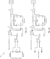
- FIG. 1A depicts a block diagram of a circuit topology 100 for sensing an analog signal through digital input/output (I/O) pins of a controller according to one or more embodiments.
- the circuit topology 100 is utilized for outputting, based on a sensed analog signal from an analog voltage circuit, a digital signal to a pin of a controller 102.
- Controller 102 can include a microcontroller, an FGPA, a digital signal processor (DSP), or another other type of controller that may conventionally include an ADC block.
- a digital I/O pin analog signal sensing architecture can include a difference amplifier A5, a comparator A4, a divideby2 counter A3, and two AND gates A1, A2.
- the divideby2 counter A3 may be implemented using a D-latch or D-flipflop.
- controller 102 is an FPGA
- one or more elements of circuit topology 100 may be programmed in to the FPGA itself to save space and cost.
- AND gates A1, A2 and divideby2 counter A3 can be programmed in to an FPGA.
- the inputs of the difference amplifier A5 may be connected to an analog voltage circuit at a location where measurements are desired to be obtained.
- the inputs of the difference amplifier A5 may be connected to either side of a resister R1 of the analog voltage circuit.
- the difference amplifier A5 may be connected to any source of analog input voltage, as shown in FIG. 1B .
- the difference amplifier may output a difference signal Vsensediff that represents the voltage difference between the two signals input into the difference amplifier A5.
- the difference amplifier A5 may amplify the difference between the input voltages to generate the output signal Vsensediff.
- the difference amplifier A5 may amplify and/or attenuate the signal in order to match an input level of comparator A4.
- the difference signal Vsensediff may be received by the non-inverting input of the comparator A4, while the inverting input of the comparator A4 may receive a triangular (or sawtooth) wave (shown as "Triangular PWL" in FIGS. 1A and 1B ).
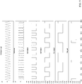
- FIG. 2 shows an example triangular wave 202 (which may also be referred to as a triangular wave signal) and difference signal 204 that may be received as inputs to comparator A4.
- the triangular wave provided as an inverting input to comparator A4 can be provided by an external source.
- the triangular wave provided to the comparator A4 acts to generate pulse width modulation (PWM) for the analog voltage senses at the resistor R1 (i.e., Vsensediff).
- PWM pulse width modulation
- the comparator A4 outputs a PWM signal based on the input variation.
- FIG. 2 illustrates an example PWM signal Vpmwout 206 that may be output by the comparator A4 based on the received triangular wave and difference signal.
- the output of the comparator A4 can be provided as a clock signal input to the Divideby2 counter A3 and as an input to AND gate A1.
- AND gate A1 may also receive a high frequency clock pulse signal Clk_in as an additional input.
- FIG. 2 shows an example high frequency clock signal 208.
- the frequency of a high frequency clock signal 208 may be so high that its periodicity may be visually imperceptible at the resolution shown in FIG. 2 , causing the signal 208 to appear as though it is a solid bar in the chart.
- the high frequency clock signal Clk_in can be provided from an existing square wave oscillator utilized for microcontroller operation or through an external reference that is required for counting purposes during a software routine.
- the AND gate A1 outputs a signal that is the superposition of the Clk_in signal on the PWM pulse signal generated by the comparator A4.
- the output of AND gate A1 and a square wave output at the Q pin of the divideby2 counter may be input into AND gate A2.
- the divideby2 counter A3 is configured to provide frequency division needed for controller logic implementation.
- the AND gate A2 outputs a resultant digital signal that includes bursts of pulses (which may also be referred to as groups of continuous pulses) to a digital I/O pin of the controller 102, which the controller may then convert to digital values based on the number of continuous pulses in each group/burst of pulses. The number of pulses in a burst represents the digital value of the input signal across R1.
- V(input_to_IOpin) signal 210 An example of the output signal of AND gate A2 is shown in FIG. 2 as V(input_to_IOpin) signal 210. Although it is imperceptible in FIG. 2 due to the resolution, it will be understood that frequency of the V(input_to_IOpin) signal is the same as that of the clock signal V(clk). As can be seen in FIG. 2 , the V(input_to_IOpin) signal provides a digital signal that represents the magnitude of the sensed analog signal by length of the pulse count.
- the V(input_to_IOpin) signal 210 shows a digital signal with a large pulse count (i.e., a bar a with thick width), which corresponds to an approximate maximum voltage in the difference signal Vsensediff 204 (i.e., the sensed analog signal), whereas at around 72 ms the V(input_to_IOpin) signal 210 shows a digital signal with a small pulse count (i.e., a bar with a thin width), which corresponds to an approximate minimum voltage in the sensed analog signal 204.
- a large pulse count i.e., a bar a with thick width
- Vsensediff 204 i.e., the sensed analog signal
- the V(input_to_IOpin) signal 210 shows a digital signal with a small pulse count (i.e., a bar with a thin width), which corresponds to an approximate minimum voltage in the sensed analog signal 204.
- 1A or 1B can generate a digital signal for input to a pin of a controller 102 that represents the sensed analog signal, based on the circuit elements provided and the use of a triangular wave and a high frequency clock signal.
- the controller 102 can convert the signal to values representative of the time-varying magnitude of the analog signal based on a count of the number of continuous pulses in each sample.
- the frequency of the high frequency clock signal Clk_in controls the resolution of the sampled signal, such that that resolution may be increased by increasing the frequency of the high frequency clock signal Clk_in.
- the triangular wave will provide the sampling interval for the input signal.
- the wave period of the triangular wave may be set based on a desired sampling interval selected by a user. Thus, in some embodiments, if frequent sampling is not needed and the sensed input signal varies slowly, it may be desirable to set the frequency of the triangular wave to be relatively lower than it would be in other situations.
- sampling interval and the resolution of the sampling interval may be modified based on modifications to the triangular wave and high frequency clock signal (clk in) respectively, the circuits and techniques described herein may allow for the sampling interval and resolution to be varied with respect to the application to be used.
- controller 102 may count the number of pulses present in the signal input to the controller 102 for each sampling interval for use in reconstructing an approximation of the sensed analog signal.
- the divideby2 counter A3 shown in FIGS. 1A and 1B can be implemented allow a software routine of the controller 102 to distinguish the next interval of sampled data.
- the software routine of the controller 102 can be written in such a way that an internal counter of the controller 102 will count each pulse included in one period duration of the triangular wave pulse and then wait for a one period duration of the triangular wave pulse before performing a subsequent count of pulses in the next period.
- the software routine can exit from the counting loop.
- FIG. 3 depicts a flow diagram of a method 300 for providing for the determination of analog values corresponding to a sensed analog signal based on a signal generated by a digital I/O pin analog signal sensing architecture according to one or more embodiments.
- the method 300 includes initializing the controller 102, as shown in block 302.
- the controller is initialized with a set of parameters to allow it to properly execute a pulse counting routine.
- the parameters can include the triangular wave pulse period, the high frequency clock (clk_in) period, the series resistor (R1) value and the high frequency clock (clk_in) pulse resolution per mV.
- the method 300 includes awaiting, by the controller 102, an input pulse.
- An input pulse is a burst of pulses at a voltage level that is acceptable by the controller 102 (e.g., typically 3.3V or 5V). Each burst includes a number of pulses (at the frequency of Clk_in) that is proportional to the input voltage across R1.
- the method includes, determining, by the controller, whether a pulse has been detected. If the controller has not detected a pulse, then the method proceeds back to block 304. If the controller does detect a pulse, then the method proceeds to block 308 in which the controller increments a pulse counter.
- the method 300 includes determining, by the counter, whether timeout has been detected.
- the controller 102 will detect a timeout when a predetermined number of clock cycles has passed without the controller 102 having detected a pulse from the signal output by the AND gate A2. For example, in some embodiments, if there has been no pulse detected for one or two clock periods than the controller 102 may determine that a timeout has occurred and proceed to block 314. The controller 102 will not detect a timeout for as long as it is continuously (i.e., in each successive clock cycle) receiving pulses. Each time (e.g., for each clock cycle) controller 102 detects a pulse, the method proceeds back to block 308 in which the controller 102 increments the pulse counter.
- the controller will repeatedly increment the pulse counter upon receiving each new pulse of the burst. Once the burst of pulses is finished, the controller 102 will determine that a timeout has occurred as described above and the method will proceed to block 314 where the controller exits the counter routine, stores the counted value in a register and computes an equivalent analog value based on the stored count. Thus, for each burst of pulses, the controller will count the number of pulses in the burst, store the value and determine an equivalent analog value corresponding to the burst of pulses. It will be understood that some bursts may only contain a single pulse, which corresponds to the least count of the digital value.
- the controller 102 may reconstruct the magnitude of the voltage of a sensed analog signal for an interval by multiplying the observed pulse count of the interval by the resolution.
- the resolution may be considered to be the smallest possible input voltage that will result in an increment on the pulse count described below and is thus represented in units of voltage per count (e.g., mV/count).
- Resolution can be calculated by dividing the maximum measurable input voltage by the maximum pulse count.
- the maximum measurable voltage is the input voltage for which the pulse count is maximum. This highest pulse count is produced when the input voltage is equal to the peak to peak voltage of the triangular wave (i.e., Vpp of the triangular wave).
- the maximum possible pulse count is the ratio of clock frequency to the triangular wave frequency.
- the resolution can be calculated as being equal to (Vpp of triangular wave)/(Fclk/Ftriangularwave) which is equivalent to (Vpp of triangular wave * Ftriangularwave)/Fclk.
- the controller 102 can reconstruct the magnitude of analog voltage for an interval by multiplying the observed pulse count during the interval by the resolution. It will be understood that the magnitude of current can alternatively be measured/determined in a manner similar to that described herein with respect to voltage.
- FIG. 4 shows an alternative embodiment of a block diagram of a circuit topology 400 for sensing an analog signal through digital input/output (I/O) pins of a controller that operates in a manner similar to that described above with respect to FIG. 1A , but instead of a divideby2 counter A3, this embodiment includes a divideby8 counter A7, divideby4 counter A6 and a divideby2 counter A3 having outputs that are AND'd together by AND gate A8 that can be used to provide an interleaved signal to the controller input.
- I/O digital input/output
- a divideby2 counter interleaves the sample to create distinct bursts of pulses. Otherwise, when a sample output reaches its full-scale value (i.e., maximum voltage reading), the controller may not be able to distinguish between that sample and the next sample, which would otherwise appear immediately after the first sample without a gap (i.e., there may be no gap between bursts of pulses that would allow the controller to distinguish between the bursts).
- the AND gate A8 will mask the logic HIGH window of the Divideby4 counter A6 and the Divideby8 counter A7 with respect to the divideby2 counter A3 output Q. The AND gate A2 will stay at logic LOW for seven consecutive cycles of triangular wave duration.
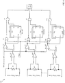
- FIG. 6 shows an alternative embodiment of a block diagram of a circuit topology 600 for sensing an analog signal through digital input/output (I/O) pins of a controller that operates in a manner similar to that described above with respect to FIG. 1A , but shows that in some embodiments, multiple of the circuits shown in FIG. 1A can be implemented together in order to obtain multiple analog readings and generate multiple input signals to different pins of the controller 102.
- I/O digital input/output
- resistors R2 and R3 perform a function similar to resistor R1
- difference amplifiers A10 and A15 perform a similar function to difference amplifier A5
- comparators A9 and A14 perform a similar function to difference amplifier A4
- divideby2 counters A8 and A13 perform a similar function to divideby2 counter A3
- first AND gates A6 and A11 perform a similar function to first AND gate A1 and second AND gates A7 and A12 perform a similar function to second AND gate A2.
- the outputs of second AND gates A2, A7 and A12 may each be connected to a separate pin of controller 102 such that the controller 102 may receive a digital signal from each ADC circuit.
- the circuit design may include up to as many ADC circuits as there are pins on the controller 102 for receiving the corresponding digital signals output by the respective ADC circuits.
- a circuit topology similar to circuit topology 600 can be formed by combining multiple of the circuits shown in FIG. 1B together in a similar manner. The configuration shown in FIG. 6 can be used to sample multiple signals simultaneously using a single Clk_in and TRIANGULAR PWL source.
- FIG. 7 depicts a flow diagram of a method for sensing an analog signal through digital input/output (I/O) pins according to one or more embodiments.
- the method 700 includes converting, via an analog digital conversion circuit (e.g., such as one of the circuits depicted in FIGS. 1 , 4 or 6 ) the analog signal into a digital signal, as shown in block 702.
- the method 700 includes receiving the digital signal via a pin of a controller (e.g., controller 102).
- the method 700 at block 706, includes counting, by the controller, pulses within the digital signal for example, in accordance with the method described above with respect to FIG. 3 .
- the method 700 includes determining, by the controller, values corresponding to the analog signal based on the counted pulses for example, in a manner similar to that described previously above.
Landscapes
- Engineering & Computer Science (AREA)
- Theoretical Computer Science (AREA)
- General Engineering & Computer Science (AREA)
- Power Engineering (AREA)
- Human Computer Interaction (AREA)
- Physics & Mathematics (AREA)
- General Physics & Mathematics (AREA)
- Analogue/Digital Conversion (AREA)
Applications Claiming Priority (1)
| Application Number | Priority Date | Filing Date | Title |
|---|---|---|---|
| IN201911024674 | 2019-06-21 |
Publications (1)
| Publication Number | Publication Date |
|---|---|
| EP3754855A1 true EP3754855A1 (fr) | 2020-12-23 |
Family
ID=68762578
Family Applications (1)
| Application Number | Title | Priority Date | Filing Date |
|---|---|---|---|
| EP19212838.7A Pending EP3754855A1 (fr) | 2019-06-21 | 2019-12-02 | Détection de signal analogique via des broches d'e/s numériques |
Country Status (4)
| Country | Link |
|---|---|
| US (1) | US10778162B1 (fr) |
| EP (1) | EP3754855A1 (fr) |
| BR (1) | BR102019026339A2 (fr) |
| CA (1) | CA3065266A1 (fr) |
Citations (2)
| Publication number | Priority date | Publication date | Assignee | Title |
|---|---|---|---|---|
| JPS5534584A (en) * | 1978-09-04 | 1980-03-11 | Advantest Corp | Analog-digital converter |
| US20030188202A1 (en) * | 2002-03-28 | 2003-10-02 | D'angelo Kevin P. | Single wire serial interface |
Family Cites Families (5)
| Publication number | Priority date | Publication date | Assignee | Title |
|---|---|---|---|---|
| JPS5299071A (en) | 1976-02-16 | 1977-08-19 | Nec Home Electronics Ltd | Production of hermetic terminals |
| US5724009A (en) * | 1996-10-29 | 1998-03-03 | Motorola Inc. | Crystal oscillator having input/output pins selectively used for analog or digital signals |
| US7138820B2 (en) | 2004-04-30 | 2006-11-21 | Xilinx, Inc. | System monitor in a programmable logic device |
| US7369078B2 (en) * | 2004-08-16 | 2008-05-06 | National Instruments Corporation | Flexible converter interface for use in analog-to-digital and digital-to-analog systems |
| US7411538B1 (en) * | 2007-03-31 | 2008-08-12 | Silicon Laboratories Inc. | SAR analog to digital converter having multiplexable ground sense pin |
-
2019
- 2019-08-16 US US16/542,664 patent/US10778162B1/en active Active
- 2019-12-02 EP EP19212838.7A patent/EP3754855A1/fr active Pending
- 2019-12-11 BR BR102019026339-3A patent/BR102019026339A2/pt unknown
- 2019-12-13 CA CA3065266A patent/CA3065266A1/fr active Pending
Patent Citations (2)
| Publication number | Priority date | Publication date | Assignee | Title |
|---|---|---|---|---|
| JPS5534584A (en) * | 1978-09-04 | 1980-03-11 | Advantest Corp | Analog-digital converter |
| US20030188202A1 (en) * | 2002-03-28 | 2003-10-02 | D'angelo Kevin P. | Single wire serial interface |
Non-Patent Citations (1)
| Title |
|---|
| WALT KESTER ET AL: "MT-026 TUTORIAL ADC Architectures VII: Counting ADCs", 31 October 2008 (2008-10-31), XP055707073, Retrieved from the Internet <URL:https://www.analog.com/media/en/training-seminars/tutorials/MT-026.pdf> [retrieved on 20200619] * |
Also Published As
| Publication number | Publication date |
|---|---|
| CA3065266A1 (fr) | 2020-12-21 |
| US10778162B1 (en) | 2020-09-15 |
| BR102019026339A2 (pt) | 2021-01-05 |
Similar Documents
| Publication | Publication Date | Title |
|---|---|---|
| JPS6166971A (ja) | デジタル抵抗測定装置とその測定方法 | |
| CN106918731A (zh) | 一种数字示波器及其信号频率测量方法 | |
| CN103901243A (zh) | 一种具有高触发精度的示波器 | |
| US10778162B1 (en) | Sensing analog signal through digital I/O pins | |
| US6950375B2 (en) | Multi-phase clock time stamping | |
| JP2000221248A (ja) | 半導体試験装置 | |
| JPH0213220A (ja) | 信号のサンプリング方法および装置この装置を用いた保護リレー装置 | |
| JP5174433B2 (ja) | Ad変換器及び秤 | |
| JP2012124774A (ja) | Ad変換装置およびda変換装置 | |
| EP3569986B1 (fr) | Dispositif de détection de position | |
| Župunski et al. | On-line determination of the measurement uncertainty of the stochastic measurement method | |
| JP6393669B2 (ja) | センサ装置及びセンシング方法 | |
| JPH0633701Y2 (ja) | オートレンジ回路 | |
| Wolffenbuttel et al. | Stochastic analog-to-digital converter based on the asynchronous sampling of a reference triangle | |
| JPH0365821A (ja) | D/aコンバータのグリッジ測定装置 | |
| JPH0654331B2 (ja) | 電力変換装置の電圧,電流検出方式 | |
| GB2227381A (en) | Analogue to digital converters | |
| JPH03270414A (ja) | D/a変換器の試験装置 | |
| Karnal et al. | A novel automatically synchronized ramp A/D converter | |
| SU712953A1 (ru) | Многоканальный преобразователь частоты в код | |
| SU1728857A2 (ru) | Многоканальное измерительное устройство | |
| JPH02196523A (ja) | Δς変調形a/d変換器の試験回路 | |
| SU1367155A1 (ru) | Аналого-цифровой преобразователь с самоконтролем | |
| KR100526864B1 (ko) | 타임측정시스템 | |
| Wang et al. | Research on Data Acquisition Module Based on Rogowski Coil ECT |
Legal Events
| Date | Code | Title | Description |
|---|---|---|---|
| PUAI | Public reference made under article 153(3) epc to a published international application that has entered the european phase |
Free format text: ORIGINAL CODE: 0009012 |
|
| STAA | Information on the status of an ep patent application or granted ep patent |
Free format text: STATUS: THE APPLICATION HAS BEEN PUBLISHED |
|
| AK | Designated contracting states |
Kind code of ref document: A1 Designated state(s): AL AT BE BG CH CY CZ DE DK EE ES FI FR GB GR HR HU IE IS IT LI LT LU LV MC MK MT NL NO PL PT RO RS SE SI SK SM TR |
|
| AX | Request for extension of the european patent |
Extension state: BA ME |
|
| STAA | Information on the status of an ep patent application or granted ep patent |
Free format text: STATUS: REQUEST FOR EXAMINATION WAS MADE |
|
| 17P | Request for examination filed |
Effective date: 20210610 |
|
| RBV | Designated contracting states (corrected) |
Designated state(s): AL AT BE BG CH CY CZ DE DK EE ES FI FR GB GR HR HU IE IS IT LI LT LU LV MC MK MT NL NO PL PT RO RS SE SI SK SM TR |
|
| STAA | Information on the status of an ep patent application or granted ep patent |
Free format text: STATUS: EXAMINATION IS IN PROGRESS |
|
| 17Q | First examination report despatched |
Effective date: 20220421 |
|
| GRAP | Despatch of communication of intention to grant a patent |
Free format text: ORIGINAL CODE: EPIDOSNIGR1 |
|
| STAA | Information on the status of an ep patent application or granted ep patent |
Free format text: STATUS: GRANT OF PATENT IS INTENDED |
|
| INTG | Intention to grant announced |
Effective date: 20260312 |