EP3760450A1 - Élément de sécurité pour un document de valeur - Google Patents
Élément de sécurité pour un document de valeur Download PDFInfo
- Publication number
- EP3760450A1 EP3760450A1 EP19184053.7A EP19184053A EP3760450A1 EP 3760450 A1 EP3760450 A1 EP 3760450A1 EP 19184053 A EP19184053 A EP 19184053A EP 3760450 A1 EP3760450 A1 EP 3760450A1
- Authority
- EP
- European Patent Office
- Prior art keywords
- layer
- oxide
- security element
- fluoride
- absorber layer
- Prior art date
- Legal status (The legal status is an assumption and is not a legal conclusion. Google has not performed a legal analysis and makes no representation as to the accuracy of the status listed.)
- Granted
Links
Images
Classifications
-
- B—PERFORMING OPERATIONS; TRANSPORTING
- B42—BOOKBINDING; ALBUMS; FILES; SPECIAL PRINTED MATTER
- B42D—BOOKS; BOOK COVERS; LOOSE LEAVES; PRINTED MATTER CHARACTERISED BY IDENTIFICATION OR SECURITY FEATURES; PRINTED MATTER OF SPECIAL FORMAT OR STYLE NOT OTHERWISE PROVIDED FOR; DEVICES FOR USE THEREWITH AND NOT OTHERWISE PROVIDED FOR; MOVABLE-STRIP WRITING OR READING APPARATUS
- B42D25/00—Information-bearing cards or sheet-like structures characterised by identification or security features; Manufacture thereof
- B42D25/30—Identification or security features, e.g. for preventing forgery
- B42D25/351—Translucent or partly translucent parts, e.g. windows
-
- B—PERFORMING OPERATIONS; TRANSPORTING
- B42—BOOKBINDING; ALBUMS; FILES; SPECIAL PRINTED MATTER
- B42D—BOOKS; BOOK COVERS; LOOSE LEAVES; PRINTED MATTER CHARACTERISED BY IDENTIFICATION OR SECURITY FEATURES; PRINTED MATTER OF SPECIAL FORMAT OR STYLE NOT OTHERWISE PROVIDED FOR; DEVICES FOR USE THEREWITH AND NOT OTHERWISE PROVIDED FOR; MOVABLE-STRIP WRITING OR READING APPARATUS
- B42D25/00—Information-bearing cards or sheet-like structures characterised by identification or security features; Manufacture thereof
- B42D25/30—Identification or security features, e.g. for preventing forgery
- B42D25/355—Security threads
Definitions
- the invention relates to a security element for a document of value, a security paper and the like, the security element having at least one color-changing thin-film element with at least one absorber layer, at least one reflector layer and at least one spacer layer arranged between the absorber layer and the reflector layer, the at least one reflector layer having at least one recess .
- the at least one spacer layer completely covers the at least one absorber layer and the reflector layer on mutually facing sides, the spacer layer also completely covering the at least one recess in the at least one reflector layer, with in In a region of the at least one recess, a color-tilting element consisting of at least the at least one absorber layer and the at least one spacer layer is formed.
- the solution according to the invention produces an additional, measurable color shift effect in the areas of the cutouts, which is not primarily recognizable to a user and, as a hidden security feature, contributes significantly to increasing the security against forgery.
- the at least one recess is designed as a letter, number, character, symbol or part of an image or pattern.
- a variant has proven to be particularly advantageous in which the at least one recess in the reflector layer is free of material from the at least one spacer layer or is at least partially filled, in particular completely filled, by at least a partial area of the at least one spacer layer.
- the at least one spacer layer extends uninterruptedly, at least over the entire length and width of the thin-film element.
- the at least one absorber layer of the thin-film element completely covers the at least one recess in the reflector layer in a plan view of the security element.
- the at least one absorber layer of the thin-film element has at least one first absorber layer completely covering the recesses of the reflector layer in a plan view of the security element and at least one second absorber layer, the at least one second absorber layer having first recesses and the at least one reflector layer has second recesses, the at least one second absorber layer between the at least one reflector layer and the at least one first absorber layer and the at least one spacer layer between the at least one reflector layer and the at least one first absorber layer and between the at least one reflector layer and the at least one second absorber layer are arranged.
- the first cutouts and the second cutouts advantageously overlap one another at least in sections, preferably completely, in a plan view of the security element.
- the at least one first absorber layer is uninterrupted and extends over the entire length and width of the thin-film element.
- the at least one first absorber layer has a degree of transmittance which is between 0.1 and 0.99, in particular between 0.5 and 0.99, particularly preferably between 0.7 and 0.99.
- the at least one reflector layer can be at least one metallic material, in particular selected from the group aluminum, silver, copper, gold, platinum, niobium, tin, or from nickel, titanium, vanadium, chromium, cobalt and palladium or alloys of these Materials, in particular cobalt-nickel alloys, or of at least one high-index dielectric material with a refractive index greater than 1.65, in particular selected from the group consisting of zinc sulfide (ZnS), zinc oxide (ZnO), titanium dioxide (TiO2), carbon (C) , Indium oxide (In 2 O 3 ), indium tin oxide (ITO), tantalum pentoxide (Ta 2 O 5 ), cerium oxide (CeO 2 ), yttrium oxide (Y 2 O 3 ), europium oxide (Eu 2 O 3 ), iron oxides such as for example (II) iron (III) oxide (Fe 3 O 4 ) and iron oxide (Fe 2
- the at least one absorber layer can contain at least one metallic material, in particular selected from the group consisting of nickel, titanium, vanadium, cobalt, palladium, iron, tungsten, molybdenum, niobium, chromium, aluminum, also silver, copper or alloys of these materials comprise and / or be made of at least one of these materials.
- the at least one spacer layer can contain at least one high-index dielectric material with a refractive index greater than or equal to 1.65, in particular selected from the group consisting of zinc sulfide (ZnS), zinc oxide (ZnO), titanium dioxide (TiO 2 ), carbon (C ), Indium oxide (In 2 O 3 ), indium tin oxide (ITO), tantalum pentoxide (Ta 2 O 5 ), cerium oxide (CeO 2 ), yttrium oxide (Y 2 O 3 ), europium oxide (Eu 2 O 3 ), iron oxides such as (II) iron (III) oxide (Fe 3 O 4 ) and iron oxide (Fe 2 O 3 ), hafnium nitride (HfN), hafnium carbide (HfC), hafnium oxide (HfO 2 ), lanthanum oxide (La 2 O 3 ), Magnesium oxide (MgO), neodymium oxide (Nd
- Na 3 AlF 6 or Na 5 Al 3 F 14 Na 3 AlF 6 or Na 5 Al 3 F 14 ), neodymium fluoride (NdF 3 ), lanthanum fluoride (LaF 3 ), samarium fluoride (SmF 3 ), barium fluoride (BaF 2 ), calcium fluoride (CaF 2 ), lithium fluoride (LiF), low-breaking organic monomers and / or comprise low-index organic polymers or from at least one of these materials be put.
- NdF 3 neodymium fluoride
- LaF 3 lanthanum fluoride
- SmF 3 samarium fluoride
- BaF 2 barium fluoride
- CaF 2 calcium fluoride
- LiF lithium fluoride
- low-breaking organic monomers and / or comprise low-index organic polymers or from at least one of these materials be put.
- At least one additional layer made of the same material as the spacer layer is arranged, the reflector layer being embedded, in particular completely, between the additional layer and the spacer layer is embedded.
- the security element has at least one carrier layer made of plastic, in particular made of a translucent plastic, which carries the at least one thin-layer element, the carrier layer preferably having at least one of the materials from the group of polyimide (PI), polypropylene (PP) , monoaxially oriented polypropylene (MOPP), biaxially oriented polypropylene (BOPP), polyethylene (PE), polyphenylene sulfide (PPS), polyetheretherketone, (PEEK) polyetherketone (PEK), polyethyleneimide (PEI), polysulfone (PSU), polyaryletherketone (PAEK), Polyethylene naphthalate (PEN), liquid crystalline polymers (LCP), polyester, polybutylene terephthalate (PBT), polyethylene terephthalate (PET), polyamide (PA), polycarbonate (PC), cycloolefin copolymers (COC), polyoxymethylene (POM), acrylonitrile butadiene st
- PI polyimide
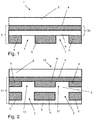
- Fig.1 shows a security element 1 according to the invention.
- This security element serves as a protection against forgery for a value document, a security paper, value cards, such as credit cards, and the like.
- the security element can be applied to the object to be secured or embedded in it.
- the security element is particularly suitable for attachment in a “window area” of the object, for example in a window area of a bank note.
- a window is understood to be a transparent area of the object.
- the security element according to the invention is not intended for use in a window area is limited, but can generally be attached in any surface area of a document of value, security paper, a value card and the like.
- the security element 1 can have a carrier layer 2 made of plastic.
- the carrier layer 2 can be made of a transparent plastic.
- plastics such as transparent carrier films, preferably flexible plastic films, for example made of polyimide (PI), polypropylene (PP), monoaxially oriented polypropylene (MOPP), biaxially oriented polypropylene (BOPP), polyethylene (PE), polyphenylene sulfide (PPS), polyether ether ketone (PEEK) Polyetherketone (PEK), Polyethyleneimide (PEI), Polysulfone (PSU), Polyaryletherketone (PAEK), Polyethylene Naphthalate (PEN), Liquid Crystalline Polymers (LCP), Polyester, Polybutylene Terephthalate (PBT), Polyethylene Terephthalate (PET), Polyamide (PA) , Polycarbonate (PC), cycloolefin copolymers (COC), polyoxymethylene (POM), acrylonitrile butadiene styrene (ABS),
- the light-permeable carrier material 14 is composed essentially of a transparent material, such as, for example, polycarbonate.
- the carrier layer preferably has a thickness of approximately 5 ⁇ m to approximately 1000 ⁇ m, particularly preferably a thickness of 10 ⁇ m-50 ⁇ m.
- a color-changing thin-film element 3 can be applied to the carrier layer 2.
- the thin-film element 3 has an absorber layer 4 and a reflector layer 5.
- a spacer layer 6 is arranged between the absorber layer 4 and the reflector layer 5.
- the reflector layer 5 has one or more cutouts 7, which can be embodied, for example, as letters, numbers, characters, symbols or as part of an image or pattern.
- cutouts 7, can be embodied, for example, as letters, numbers, characters, symbols or as part of an image or pattern.
- the spacer layer 6 covers the absorber layer 4 and the reflector layer 5 over the entire surface on mutually facing sides of these layers.
- the cutouts 7 in the reflector layer 5 are also covered by the spacer layer 6.
- the recess 7 in the reflector layer can also be partially or completely filled in by subregions of the spacer layer 6.
- the spacer layer 6 can extend over the entire length and width of the thin-film element 3 without interruptions in the layer.
- a color-tilting element 3a consisting of the absorber layer 4 and the spacer layer 6 is formed.
- the color-shifting element 3a formed from the spacer layer 6 and the absorber layer 4 generates a second color-shifting effect in the areas of the recesses 7 in addition to a first color-shifting element formed from the absorber layer 4, the spacer layer 6 and the full-area, uninterrupted areas of the reflector layer 5.
- the first color shift effect can be seen here with the naked eye, while the second color shift effect is significantly weaker due to the lack of reflector layer 5 and can at least be detected by machine.
- the absorber layer 4 of the thin-film element 3 can completely cover the recesses 7 of or in the reflector layer 5 in a plan view of the security element 1.
- the absorber layer 4, viewed from the direction of the carrier layer 2 can completely cover the recesses 7, the recesses 7, viewed from the direction of the carrier layer 2, lying behind the absorber layer 4.
- the absorber layer 4 is preferably made from a metal, for example from nickel, titanium, vanadium, cobalt, palladium, iron, tungsten, molybdenum, niobium, chromium, aluminum, copper or silver or from alloys of these materials.
- the absorber layer 4 can, for example, have a transmission coefficient which is between 0.1 and 0.99, in particular between 0.5 and 0.99, particularly preferably between 0.7 and 0.99.
- the spacer layer is usually made of a dielectric material.
- the spacer layer can be made from a material with a low refractive index, for example a refractive index less than or equal to 1.65.
- Suitable materials with a low refractive index are, for example, silicon oxide (SIO x ), silicon dioxide (SiO 2 ), aluminum oxide (Al 2 O 3 ), metal fluorides, for example magnesium fluoride (MgF 2 ), aluminum fluoride (AlF 3 ), cerium fluoride (CeF 3 ), sodium -Aluminum fluoride (e.g.
- Na 3 AlF 6 or Na 5 Al 3 F 14 Na 3 AlF 6 or Na 5 Al 3 F 14 ), neodymium fluoride (NdF 3 ), lanthanum fluoride (LaF 3 ), samarium fluoride (SmF 3 ) barium fluoride (BaF 2 ), calcium fluoride (CaF 2 ), lithium fluoride (LiF), or Combinations of these materials.
- NdF 3 neodymium fluoride
- LaF 3 lanthanum fluoride
- SmF 3 samarium fluoride barium fluoride
- BaF 2 calcium fluoride
- LiF lithium fluoride
- the spacer layer can also be made from a material with a high refractive index, for example a refractive index greater than 1.65.
- Suitable materials with a high refractive index are, for example, zinc sulfide (ZnS), zinc oxide (ZnO), titanium dioxide (TiO2), carbon (C), indium oxide (In 2 O 3 ), indium tin oxide (ITO), tantalum pentoxide (Ta 2 O) 5 ), cerium oxide (CeO2), yttrium oxide (Y 2 O 3 ), europium oxide (Eu 2 O 3 ), iron oxides such as (II) iron (III) oxide (Fe 3 O 4 ) and iron oxide (Fe 2 O 3 ) , Hafnium nitride (HfN), hafnium carbide (HfC), hafnium oxide (HfO 2 ), lanthanum oxide (La 2 O 3 ), magnesium oxide (MgO), neodym
- ZnS zinc
- the layer thickness of the spacer layer 6 is preferably 50 nm to 800 nm, in particular between 100 nm to 700 nm, particularly preferably 150 to 600 nm.
- the spacer layer 6 can have an optical thickness depending on the desired color shift give in Quarter Wave Optical Thinkness (QWOT) from about 2 QWOT at a wavelength of 400 nm to about 9 QWOT at a wavelength of about 700 nm, preferably the spacer layer 6 at 400-700 nm has an optical thickness of 2-6 QWOT on.
- QWOT Quarter Wave Optical Thinkness
- the stated values are not just about ranges of variation, but the thickness of the layer 6 is different depending on the color shift effect to be achieved in each case.
- the reflector layer 5 can, for example, be made of metals such as aluminum, silver, copper, gold, platinum, niobium, tin, or of nickel, titanium, chromium, vanadium, cobalt and palladium or cobalt-nickel alloys.
- the reflective layer can also consist of a high-index dielectric layer with a refractive index of greater than 1.65, in particular selected from the group consisting of zinc sulfide (ZnS), zinc oxide (ZnO), titanium dioxide (TiO 2 ), carbon (C) , Indium oxide (In 2 O 3 ), indium tin oxide (ITO), tantalum pentoxide (Ta 2 O 5 ), cerium oxide (CeO 2 ), yttrium oxide (Y 2 O 3 ), europium oxide (Eu 2 O 3 ), iron oxides such as for example (II) iron (III) oxide (Fe 3 O 4 ) and Iron oxide (Fe 2 O 3 ), hafnium nitride (HfN), hafnium carbide (HfC), hafnium oxide (HfO 2 ), lanthanum oxide (La 2 O 3 ), magnesium oxide (MgO), neodymium oxide (Nd 2 O 3 ),
- ZnS zinc s
- an optical density (OD) of the reflector layer 5 is preferably between 1 and 3, preferably between 1.5 and 2.5%.
- the reflector layer 5 can be quasi-transparent.
- the spacer layer 6 is made from a dielectric material with a low refractive index and the reflective layer is made from a dielectric material with a high refractive index.
- the absorber layer of the thin-film element 11 of the security element 10 can have at least one first absorber layer 4, which completely covers the recesses 7 of the reflector layer 5 in a plan view of the security element 10, and a second absorber layer 8 that is applied to the first absorber layer 4.
- the second absorber layer 8 can be applied partially to the first absorber layer 4 and have first cutouts 12, the reflector layer 5 having second cutouts 7.
- the second absorber layer 8 lies between the reflector layer 5 and the first absorber layer 4.
- the spacer layer 6 is arranged between the reflector layer 5 and the first absorber layer 4 and between the reflector layer 5 and the second absorber layer 8.
- the second absorber layer 8 preferably has an optical density (OD) of 0.1-0.9, in particular 0.3-0.4, and can be made from the same materials as the first absorber layer 4.
- the first cutouts 12 and the second cutouts 7 can overlap in sections in a plan view of the security element 1.
- the first cutouts 12 and the second cutouts 7 preferably completely overlap.
- the first cutouts 12 and the second cutouts 7 can be designed to be congruent to one another.
- Fig. 2 As can also be seen, on a side of the reflector layer 5 facing away from the spacer layer 6, at least one further layer 9 made of the same material as the spacer layer 6 can be arranged. After the layer 9 has been applied, it directly adjoins the spacer layer 6 in areas of the cutouts 12 or merges into it.
- the reflector layer 5 can be embedded, in particular completely embedded, between the further layer 9 and the spacer layer 6.
- the layer 9 preferably has a layer thickness between 100 nm and 400 nm, in particular between 150 nm and 300 nm, particularly preferably between 160 and 200 nm.
- washing paint can be applied in the areas in which the second absorber layer 8 should have the cutouts 12.
- the second absorber layer 8 can be applied to this and the washing color can be removed, as a result of which the recesses 12 remain as demetallized areas.
- a coating with the spacer layer 6 can then take place.
- Wash paint can in turn be applied to the spacer layer 6 in areas in which the reflector layer 5 is to have the recesses 7. After the spacer layer 6 has been coated with the reflector layer 5, the washing color can be removed so that the recesses 7 remain as demetallized areas.
- the layer 9 can then be applied to the reflector layer, as a result of which the recesses 7 in the reflector layer 5 are completely or partially filled with the material of the layer 9.
- the recesses 7 in the reflector layer 5 can also be left unfilled, so that no material is present in the recesses.
- first absorber layer 4 and the second absorber layer 8 can be designed as a single absorber layer with a varying layer thickness, onto which the spacer layer 6 and, if appropriate, the washing paint and the reflector layer 5 are applied in the course of production be applied. It should also be pointed out that the spacer layer 6 and the layer 9 can also form a single continuous layer.
- the individual layers can be applied to one another in a manner known per se, for example by means of physical vapor deposition (PVD) processes, sputtering or by means of printing processes.
- PVD physical vapor deposition
- the absorber layer 8 and the reflector layer 5 can only be partially applied or produced by means of etching processes.
- the security element 1 can be produced analogously to the method described above.
Landscapes
- Laminated Bodies (AREA)
Priority Applications (2)
| Application Number | Priority Date | Filing Date | Title |
|---|---|---|---|
| EP19184053.7A EP3760450B1 (fr) | 2019-07-03 | 2019-07-03 | Élément de sécurité pour un document de valeur |
| PCT/EP2020/068649 WO2021001475A1 (fr) | 2019-07-03 | 2020-07-02 | Élément de sécurité pour un document de valeur |
Applications Claiming Priority (1)
| Application Number | Priority Date | Filing Date | Title |
|---|---|---|---|
| EP19184053.7A EP3760450B1 (fr) | 2019-07-03 | 2019-07-03 | Élément de sécurité pour un document de valeur |
Publications (3)
| Publication Number | Publication Date |
|---|---|
| EP3760450A1 true EP3760450A1 (fr) | 2021-01-06 |
| EP3760450C0 EP3760450C0 (fr) | 2024-03-06 |
| EP3760450B1 EP3760450B1 (fr) | 2024-03-06 |
Family
ID=67145668
Family Applications (1)
| Application Number | Title | Priority Date | Filing Date |
|---|---|---|---|
| EP19184053.7A Active EP3760450B1 (fr) | 2019-07-03 | 2019-07-03 | Élément de sécurité pour un document de valeur |
Country Status (2)
| Country | Link |
|---|---|
| EP (1) | EP3760450B1 (fr) |
| WO (1) | WO2021001475A1 (fr) |
Citations (2)
| Publication number | Priority date | Publication date | Assignee | Title |
|---|---|---|---|---|
| WO2004097112A1 (fr) * | 2003-04-28 | 2004-11-11 | Giesecke & Devrient Gmbh | Element de securite plan et son procede de fabrication |
| DE102004049118A1 (de) * | 2004-10-07 | 2006-04-13 | Giesecke & Devrient Gmbh | Sicherheitselement und Verfahren zu seiner Herstellung |
-
2019
- 2019-07-03 EP EP19184053.7A patent/EP3760450B1/fr active Active
-
2020
- 2020-07-02 WO PCT/EP2020/068649 patent/WO2021001475A1/fr not_active Ceased
Patent Citations (2)
| Publication number | Priority date | Publication date | Assignee | Title |
|---|---|---|---|---|
| WO2004097112A1 (fr) * | 2003-04-28 | 2004-11-11 | Giesecke & Devrient Gmbh | Element de securite plan et son procede de fabrication |
| DE102004049118A1 (de) * | 2004-10-07 | 2006-04-13 | Giesecke & Devrient Gmbh | Sicherheitselement und Verfahren zu seiner Herstellung |
Also Published As
| Publication number | Publication date |
|---|---|
| WO2021001475A1 (fr) | 2021-01-07 |
| EP3760450C0 (fr) | 2024-03-06 |
| EP3760450B1 (fr) | 2024-03-06 |
Similar Documents
| Publication | Publication Date | Title |
|---|---|---|
| EP4140760A1 (fr) | Marque de sûreté pour documents de valeur ou documents de sécurité | |
| EP3800060A1 (fr) | Élément de sécurité pourvu d'au moins une première zone à inversement de couleurs | |
| WO2022129207A1 (fr) | Élément de sécurité à signes réfléchissantes et statiques | |
| EP3760450B1 (fr) | Élément de sécurité pour un document de valeur | |
| AT523814B1 (de) | Sicherheitselement | |
| WO2024011272A1 (fr) | Élément de sécurité | |
| EP4306328A1 (fr) | Élément de sécurité | |
| WO2024130289A2 (fr) | Élément de sécurité | |
| EP3778256B1 (fr) | Élément de sécurité | |
| EP4242009B1 (fr) | Élément de sécurité pour documents de valeur doté d'une feuille de support et d'au moins une couche décorative | |
| WO2022069486A1 (fr) | Substrat pour la production de papiers de valeur ou de papiers de sécurité | |
| WO2022018077A1 (fr) | Élément de sécurité pour papier de valeur | |
| EP4306329A1 (fr) | Élément de sécurité | |
| EP3800061A1 (fr) | Élément de sécurité doté d'une couche à effet optique | |
| EP4121299A1 (fr) | Élément de sécurité plat présentant des caractéristiques de sécurité optique | |
| EP3929000B1 (fr) | Élément de sécurité pour titres ou papiers de sécurité | |
| EP4275912A1 (fr) | Élément de sécurité | |
| EP3800062A1 (fr) | Élément de sécurité doté d'une couche à effet optique conçue sous la forme d'élément à couche mince | |
| EP4420890A1 (fr) | Substrat doté d'une couche électroconductrice | |
| EP4275911A1 (fr) | Élément de sécurité | |
| EP4538049A1 (fr) | Élément de sécurité à structure en relief | |
| EP4420889A1 (fr) | Élément de sécurité comprenant une couche électroconductrice | |
| EP4538048A1 (fr) | Élément de sécurité doté de structures | |
| EP4585423A1 (fr) | Élément de sécurité avec des ouvertures de motifs et zone d'interruption | |
| EP4389443A1 (fr) | Élément de sécurité |
Legal Events
| Date | Code | Title | Description |
|---|---|---|---|
| PUAI | Public reference made under article 153(3) epc to a published international application that has entered the european phase |
Free format text: ORIGINAL CODE: 0009012 |
|
| STAA | Information on the status of an ep patent application or granted ep patent |
Free format text: STATUS: THE APPLICATION HAS BEEN PUBLISHED |
|
| AK | Designated contracting states |
Kind code of ref document: A1 Designated state(s): AL AT BE BG CH CY CZ DE DK EE ES FI FR GB GR HR HU IE IS IT LI LT LU LV MC MK MT NL NO PL PT RO RS SE SI SK SM TR |
|
| AX | Request for extension of the european patent |
Extension state: BA ME |
|
| STAA | Information on the status of an ep patent application or granted ep patent |
Free format text: STATUS: REQUEST FOR EXAMINATION WAS MADE |
|
| 17P | Request for examination filed |
Effective date: 20210705 |
|
| RBV | Designated contracting states (corrected) |
Designated state(s): AL AT BE BG CH CY CZ DE DK EE ES FI FR GB GR HR HU IE IS IT LI LT LU LV MC MK MT NL NO PL PT RO RS SE SI SK SM TR |
|
| STAA | Information on the status of an ep patent application or granted ep patent |
Free format text: STATUS: EXAMINATION IS IN PROGRESS |
|
| 17Q | First examination report despatched |
Effective date: 20220112 |
|
| GRAP | Despatch of communication of intention to grant a patent |
Free format text: ORIGINAL CODE: EPIDOSNIGR1 |
|
| STAA | Information on the status of an ep patent application or granted ep patent |
Free format text: STATUS: GRANT OF PATENT IS INTENDED |
|
| INTG | Intention to grant announced |
Effective date: 20230929 |
|
| GRAS | Grant fee paid |
Free format text: ORIGINAL CODE: EPIDOSNIGR3 |
|
| GRAA | (expected) grant |
Free format text: ORIGINAL CODE: 0009210 |
|
| STAA | Information on the status of an ep patent application or granted ep patent |
Free format text: STATUS: THE PATENT HAS BEEN GRANTED |
|
| AK | Designated contracting states |
Kind code of ref document: B1 Designated state(s): AL AT BE BG CH CY CZ DE DK EE ES FI FR GB GR HR HU IE IS IT LI LT LU LV MC MK MT NL NO PL PT RO RS SE SI SK SM TR |
|
| REG | Reference to a national code |
Ref country code: CH Ref legal event code: EP |
|
| REG | Reference to a national code |
Ref country code: DE Ref legal event code: R096 Ref document number: 502019010716 Country of ref document: DE |
|
| REG | Reference to a national code |
Ref country code: IE Ref legal event code: FG4D Free format text: LANGUAGE OF EP DOCUMENT: GERMAN |
|
| U01 | Request for unitary effect filed |
Effective date: 20240405 |
|
| U07 | Unitary effect registered |
Designated state(s): AT BE BG DE DK EE FI FR IT LT LU LV MT NL PT SE SI Effective date: 20240412 |
|
| PG25 | Lapsed in a contracting state [announced via postgrant information from national office to epo] |
Ref country code: GR Free format text: LAPSE BECAUSE OF FAILURE TO SUBMIT A TRANSLATION OF THE DESCRIPTION OR TO PAY THE FEE WITHIN THE PRESCRIBED TIME-LIMIT Effective date: 20240607 |
|
| PG25 | Lapsed in a contracting state [announced via postgrant information from national office to epo] |
Ref country code: RS Free format text: LAPSE BECAUSE OF FAILURE TO SUBMIT A TRANSLATION OF THE DESCRIPTION OR TO PAY THE FEE WITHIN THE PRESCRIBED TIME-LIMIT Effective date: 20240606 Ref country code: HR Free format text: LAPSE BECAUSE OF FAILURE TO SUBMIT A TRANSLATION OF THE DESCRIPTION OR TO PAY THE FEE WITHIN THE PRESCRIBED TIME-LIMIT Effective date: 20240306 |
|
| PG25 | Lapsed in a contracting state [announced via postgrant information from national office to epo] |
Ref country code: ES Free format text: LAPSE BECAUSE OF FAILURE TO SUBMIT A TRANSLATION OF THE DESCRIPTION OR TO PAY THE FEE WITHIN THE PRESCRIBED TIME-LIMIT Effective date: 20240306 |
|
| PG25 | Lapsed in a contracting state [announced via postgrant information from national office to epo] |
Ref country code: RS Free format text: LAPSE BECAUSE OF FAILURE TO SUBMIT A TRANSLATION OF THE DESCRIPTION OR TO PAY THE FEE WITHIN THE PRESCRIBED TIME-LIMIT Effective date: 20240606 Ref country code: NO Free format text: LAPSE BECAUSE OF FAILURE TO SUBMIT A TRANSLATION OF THE DESCRIPTION OR TO PAY THE FEE WITHIN THE PRESCRIBED TIME-LIMIT Effective date: 20240606 Ref country code: HR Free format text: LAPSE BECAUSE OF FAILURE TO SUBMIT A TRANSLATION OF THE DESCRIPTION OR TO PAY THE FEE WITHIN THE PRESCRIBED TIME-LIMIT Effective date: 20240306 Ref country code: GR Free format text: LAPSE BECAUSE OF FAILURE TO SUBMIT A TRANSLATION OF THE DESCRIPTION OR TO PAY THE FEE WITHIN THE PRESCRIBED TIME-LIMIT Effective date: 20240607 Ref country code: ES Free format text: LAPSE BECAUSE OF FAILURE TO SUBMIT A TRANSLATION OF THE DESCRIPTION OR TO PAY THE FEE WITHIN THE PRESCRIBED TIME-LIMIT Effective date: 20240306 |
|
| U20 | Renewal fee for the european patent with unitary effect paid |
Year of fee payment: 6 Effective date: 20240726 |
|
| PG25 | Lapsed in a contracting state [announced via postgrant information from national office to epo] |
Ref country code: IS Free format text: LAPSE BECAUSE OF FAILURE TO SUBMIT A TRANSLATION OF THE DESCRIPTION OR TO PAY THE FEE WITHIN THE PRESCRIBED TIME-LIMIT Effective date: 20240706 |
|
| PG25 | Lapsed in a contracting state [announced via postgrant information from national office to epo] |
Ref country code: SM Free format text: LAPSE BECAUSE OF FAILURE TO SUBMIT A TRANSLATION OF THE DESCRIPTION OR TO PAY THE FEE WITHIN THE PRESCRIBED TIME-LIMIT Effective date: 20240306 |
|
| PGFP | Annual fee paid to national office [announced via postgrant information from national office to epo] |
Ref country code: GB Payment date: 20240725 Year of fee payment: 6 |
|
| PG25 | Lapsed in a contracting state [announced via postgrant information from national office to epo] |
Ref country code: CZ Free format text: LAPSE BECAUSE OF FAILURE TO SUBMIT A TRANSLATION OF THE DESCRIPTION OR TO PAY THE FEE WITHIN THE PRESCRIBED TIME-LIMIT Effective date: 20240306 |
|
| PG25 | Lapsed in a contracting state [announced via postgrant information from national office to epo] |
Ref country code: PL Free format text: LAPSE BECAUSE OF FAILURE TO SUBMIT A TRANSLATION OF THE DESCRIPTION OR TO PAY THE FEE WITHIN THE PRESCRIBED TIME-LIMIT Effective date: 20240306 |
|
| PG25 | Lapsed in a contracting state [announced via postgrant information from national office to epo] |
Ref country code: SK Free format text: LAPSE BECAUSE OF FAILURE TO SUBMIT A TRANSLATION OF THE DESCRIPTION OR TO PAY THE FEE WITHIN THE PRESCRIBED TIME-LIMIT Effective date: 20240306 |
|
| PG25 | Lapsed in a contracting state [announced via postgrant information from national office to epo] |
Ref country code: SM Free format text: LAPSE BECAUSE OF FAILURE TO SUBMIT A TRANSLATION OF THE DESCRIPTION OR TO PAY THE FEE WITHIN THE PRESCRIBED TIME-LIMIT Effective date: 20240306 Ref country code: SK Free format text: LAPSE BECAUSE OF FAILURE TO SUBMIT A TRANSLATION OF THE DESCRIPTION OR TO PAY THE FEE WITHIN THE PRESCRIBED TIME-LIMIT Effective date: 20240306 Ref country code: RO Free format text: LAPSE BECAUSE OF FAILURE TO SUBMIT A TRANSLATION OF THE DESCRIPTION OR TO PAY THE FEE WITHIN THE PRESCRIBED TIME-LIMIT Effective date: 20240306 Ref country code: PL Free format text: LAPSE BECAUSE OF FAILURE TO SUBMIT A TRANSLATION OF THE DESCRIPTION OR TO PAY THE FEE WITHIN THE PRESCRIBED TIME-LIMIT Effective date: 20240306 Ref country code: IS Free format text: LAPSE BECAUSE OF FAILURE TO SUBMIT A TRANSLATION OF THE DESCRIPTION OR TO PAY THE FEE WITHIN THE PRESCRIBED TIME-LIMIT Effective date: 20240706 Ref country code: CZ Free format text: LAPSE BECAUSE OF FAILURE TO SUBMIT A TRANSLATION OF THE DESCRIPTION OR TO PAY THE FEE WITHIN THE PRESCRIBED TIME-LIMIT Effective date: 20240306 |
|
| REG | Reference to a national code |
Ref country code: DE Ref legal event code: R097 Ref document number: 502019010716 Country of ref document: DE |
|
| PLBE | No opposition filed within time limit |
Free format text: ORIGINAL CODE: 0009261 |
|
| STAA | Information on the status of an ep patent application or granted ep patent |
Free format text: STATUS: NO OPPOSITION FILED WITHIN TIME LIMIT |
|
| PG25 | Lapsed in a contracting state [announced via postgrant information from national office to epo] |
Ref country code: MC Free format text: LAPSE BECAUSE OF FAILURE TO SUBMIT A TRANSLATION OF THE DESCRIPTION OR TO PAY THE FEE WITHIN THE PRESCRIBED TIME-LIMIT Effective date: 20240306 |
|
| 26N | No opposition filed |
Effective date: 20241209 |
|
| REG | Reference to a national code |
Ref country code: CH Ref legal event code: PL |
|
| PG25 | Lapsed in a contracting state [announced via postgrant information from national office to epo] |
Ref country code: CH Free format text: LAPSE BECAUSE OF NON-PAYMENT OF DUE FEES Effective date: 20240731 |
|
| PG25 | Lapsed in a contracting state [announced via postgrant information from national office to epo] |
Ref country code: IE Free format text: LAPSE BECAUSE OF NON-PAYMENT OF DUE FEES Effective date: 20240703 |
|
| PG25 | Lapsed in a contracting state [announced via postgrant information from national office to epo] |
Ref country code: CY Free format text: LAPSE BECAUSE OF FAILURE TO SUBMIT A TRANSLATION OF THE DESCRIPTION OR TO PAY THE FEE WITHIN THE PRESCRIBED TIME-LIMIT; INVALID AB INITIO Effective date: 20190703 |
|
| PG25 | Lapsed in a contracting state [announced via postgrant information from national office to epo] |
Ref country code: HU Free format text: LAPSE BECAUSE OF FAILURE TO SUBMIT A TRANSLATION OF THE DESCRIPTION OR TO PAY THE FEE WITHIN THE PRESCRIBED TIME-LIMIT; INVALID AB INITIO Effective date: 20190703 |
|
| GBPC | Gb: european patent ceased through non-payment of renewal fee |
Effective date: 20250703 |
|
| U90 | Renewal fees not paid: noting of loss of rights |
Free format text: RENEWAL FEE NOT PAID FOR YEAR 07 Effective date: 20260224 |
|
| PG25 | Lapsed in a contracting state [announced via postgrant information from national office to epo] |
Ref country code: GB Free format text: LAPSE BECAUSE OF NON-PAYMENT OF DUE FEES Effective date: 20250703 |