EP3769162B1 - Herstellungsverfahren von uhrkomponenten aus silizium - Google Patents
Herstellungsverfahren von uhrkomponenten aus silizium Download PDFInfo
- Publication number
- EP3769162B1 EP3769162B1 EP19717200.0A EP19717200A EP3769162B1 EP 3769162 B1 EP3769162 B1 EP 3769162B1 EP 19717200 A EP19717200 A EP 19717200A EP 3769162 B1 EP3769162 B1 EP 3769162B1
- Authority
- EP
- European Patent Office
- Prior art keywords
- wafer
- components
- silicon
- timepiece components
- timepiece
- Prior art date
- Legal status (The legal status is an assumption and is not a legal conclusion. Google has not performed a legal analysis and makes no representation as to the accuracy of the status listed.)
- Active
Links
Images

Classifications
-
- G—PHYSICS
- G04—HOROLOGY
- G04B—MECHANICALLY-DRIVEN CLOCKS OR WATCHES; MECHANICAL PARTS OF CLOCKS OR WATCHES IN GENERAL; TIME PIECES USING THE POSITION OF THE SUN, MOON OR STARS
- G04B17/00—Mechanisms for stabilising frequency
- G04B17/20—Compensation of mechanisms for stabilising frequency
- G04B17/22—Compensation of mechanisms for stabilising frequency for the effect of variations of temperature
- G04B17/227—Compensation of mechanisms for stabilising frequency for the effect of variations of temperature composition and manufacture of the material used
-
- C—CHEMISTRY; METALLURGY
- C01—INORGANIC CHEMISTRY
- C01B—NON-METALLIC ELEMENTS; COMPOUNDS THEREOF; METALLOIDS OR COMPOUNDS THEREOF NOT COVERED BY SUBCLASS C01C
- C01B33/00—Silicon; Compounds thereof
- C01B33/02—Silicon
-
- C—CHEMISTRY; METALLURGY
- C23—COATING METALLIC MATERIAL; COATING MATERIAL WITH METALLIC MATERIAL; CHEMICAL SURFACE TREATMENT; DIFFUSION TREATMENT OF METALLIC MATERIAL; COATING BY VACUUM EVAPORATION, BY SPUTTERING, BY ION IMPLANTATION OR BY CHEMICAL VAPOUR DEPOSITION, IN GENERAL; INHIBITING CORROSION OF METALLIC MATERIAL OR INCRUSTATION IN GENERAL
- C23C—COATING METALLIC MATERIAL; COATING MATERIAL WITH METALLIC MATERIAL; SURFACE TREATMENT OF METALLIC MATERIAL BY DIFFUSION INTO THE SURFACE, BY CHEMICAL CONVERSION OR SUBSTITUTION; COATING BY VACUUM EVAPORATION, BY SPUTTERING, BY ION IMPLANTATION OR BY CHEMICAL VAPOUR DEPOSITION, IN GENERAL
- C23C14/00—Coating by vacuum evaporation, by sputtering or by ion implantation of the coating forming material
- C23C14/06—Coating by vacuum evaporation, by sputtering or by ion implantation of the coating forming material characterised by the coating material
- C23C14/08—Oxides
-
- C—CHEMISTRY; METALLURGY
- C23—COATING METALLIC MATERIAL; COATING MATERIAL WITH METALLIC MATERIAL; CHEMICAL SURFACE TREATMENT; DIFFUSION TREATMENT OF METALLIC MATERIAL; COATING BY VACUUM EVAPORATION, BY SPUTTERING, BY ION IMPLANTATION OR BY CHEMICAL VAPOUR DEPOSITION, IN GENERAL; INHIBITING CORROSION OF METALLIC MATERIAL OR INCRUSTATION IN GENERAL
- C23C—COATING METALLIC MATERIAL; COATING MATERIAL WITH METALLIC MATERIAL; SURFACE TREATMENT OF METALLIC MATERIAL BY DIFFUSION INTO THE SURFACE, BY CHEMICAL CONVERSION OR SUBSTITUTION; COATING BY VACUUM EVAPORATION, BY SPUTTERING, BY ION IMPLANTATION OR BY CHEMICAL VAPOUR DEPOSITION, IN GENERAL
- C23C14/00—Coating by vacuum evaporation, by sputtering or by ion implantation of the coating forming material
- C23C14/06—Coating by vacuum evaporation, by sputtering or by ion implantation of the coating forming material characterised by the coating material
- C23C14/10—Glass or silica
-
- C—CHEMISTRY; METALLURGY
- C23—COATING METALLIC MATERIAL; COATING MATERIAL WITH METALLIC MATERIAL; CHEMICAL SURFACE TREATMENT; DIFFUSION TREATMENT OF METALLIC MATERIAL; COATING BY VACUUM EVAPORATION, BY SPUTTERING, BY ION IMPLANTATION OR BY CHEMICAL VAPOUR DEPOSITION, IN GENERAL; INHIBITING CORROSION OF METALLIC MATERIAL OR INCRUSTATION IN GENERAL
- C23C—COATING METALLIC MATERIAL; COATING MATERIAL WITH METALLIC MATERIAL; SURFACE TREATMENT OF METALLIC MATERIAL BY DIFFUSION INTO THE SURFACE, BY CHEMICAL CONVERSION OR SUBSTITUTION; COATING BY VACUUM EVAPORATION, BY SPUTTERING, BY ION IMPLANTATION OR BY CHEMICAL VAPOUR DEPOSITION, IN GENERAL
- C23C16/00—Chemical coating by decomposition of gaseous compounds, without leaving reaction products of surface material in the coating, i.e. chemical vapour deposition [CVD] processes
- C23C16/22—Chemical coating by decomposition of gaseous compounds, without leaving reaction products of surface material in the coating, i.e. chemical vapour deposition [CVD] processes characterised by the deposition of inorganic material, other than metallic material
- C23C16/30—Deposition of compounds, mixtures or solid solutions, e.g. borides, carbides, nitrides
- C23C16/40—Oxides
- C23C16/401—Oxides containing silicon
-
- C—CHEMISTRY; METALLURGY
- C23—COATING METALLIC MATERIAL; COATING MATERIAL WITH METALLIC MATERIAL; CHEMICAL SURFACE TREATMENT; DIFFUSION TREATMENT OF METALLIC MATERIAL; COATING BY VACUUM EVAPORATION, BY SPUTTERING, BY ION IMPLANTATION OR BY CHEMICAL VAPOUR DEPOSITION, IN GENERAL; INHIBITING CORROSION OF METALLIC MATERIAL OR INCRUSTATION IN GENERAL
- C23C—COATING METALLIC MATERIAL; COATING MATERIAL WITH METALLIC MATERIAL; SURFACE TREATMENT OF METALLIC MATERIAL BY DIFFUSION INTO THE SURFACE, BY CHEMICAL CONVERSION OR SUBSTITUTION; COATING BY VACUUM EVAPORATION, BY SPUTTERING, BY ION IMPLANTATION OR BY CHEMICAL VAPOUR DEPOSITION, IN GENERAL
- C23C16/00—Chemical coating by decomposition of gaseous compounds, without leaving reaction products of surface material in the coating, i.e. chemical vapour deposition [CVD] processes
- C23C16/22—Chemical coating by decomposition of gaseous compounds, without leaving reaction products of surface material in the coating, i.e. chemical vapour deposition [CVD] processes characterised by the deposition of inorganic material, other than metallic material
- C23C16/30—Deposition of compounds, mixtures or solid solutions, e.g. borides, carbides, nitrides
- C23C16/40—Oxides
- C23C16/401—Oxides containing silicon
- C23C16/402—Silicon dioxide
-
- C—CHEMISTRY; METALLURGY
- C30—CRYSTAL GROWTH
- C30B—SINGLE-CRYSTAL GROWTH; UNIDIRECTIONAL SOLIDIFICATION OF EUTECTIC MATERIAL OR UNIDIRECTIONAL DEMIXING OF EUTECTOID MATERIAL; REFINING BY ZONE-MELTING OF MATERIAL; PRODUCTION OF A HOMOGENEOUS POLYCRYSTALLINE MATERIAL WITH DEFINED STRUCTURE; SINGLE CRYSTALS OR HOMOGENEOUS POLYCRYSTALLINE MATERIAL WITH DEFINED STRUCTURE; AFTER-TREATMENT OF SINGLE CRYSTALS OR A HOMOGENEOUS POLYCRYSTALLINE MATERIAL WITH DEFINED STRUCTURE; APPARATUS THEREFOR
- C30B29/00—Single crystals or homogeneous polycrystalline material with defined structure characterised by the material or by their shape
- C30B29/02—Elements
- C30B29/06—Silicon
-
- C—CHEMISTRY; METALLURGY
- C30—CRYSTAL GROWTH
- C30B—SINGLE-CRYSTAL GROWTH; UNIDIRECTIONAL SOLIDIFICATION OF EUTECTIC MATERIAL OR UNIDIRECTIONAL DEMIXING OF EUTECTOID MATERIAL; REFINING BY ZONE-MELTING OF MATERIAL; PRODUCTION OF A HOMOGENEOUS POLYCRYSTALLINE MATERIAL WITH DEFINED STRUCTURE; SINGLE CRYSTALS OR HOMOGENEOUS POLYCRYSTALLINE MATERIAL WITH DEFINED STRUCTURE; AFTER-TREATMENT OF SINGLE CRYSTALS OR A HOMOGENEOUS POLYCRYSTALLINE MATERIAL WITH DEFINED STRUCTURE; APPARATUS THEREFOR
- C30B33/00—After-treatment of single crystals or homogeneous polycrystalline material with defined structure
- C30B33/005—Oxydation
-
- C—CHEMISTRY; METALLURGY
- C30—CRYSTAL GROWTH
- C30B—SINGLE-CRYSTAL GROWTH; UNIDIRECTIONAL SOLIDIFICATION OF EUTECTIC MATERIAL OR UNIDIRECTIONAL DEMIXING OF EUTECTOID MATERIAL; REFINING BY ZONE-MELTING OF MATERIAL; PRODUCTION OF A HOMOGENEOUS POLYCRYSTALLINE MATERIAL WITH DEFINED STRUCTURE; SINGLE CRYSTALS OR HOMOGENEOUS POLYCRYSTALLINE MATERIAL WITH DEFINED STRUCTURE; AFTER-TREATMENT OF SINGLE CRYSTALS OR A HOMOGENEOUS POLYCRYSTALLINE MATERIAL WITH DEFINED STRUCTURE; APPARATUS THEREFOR
- C30B33/00—After-treatment of single crystals or homogeneous polycrystalline material with defined structure
- C30B33/02—Heat treatment
-
- C—CHEMISTRY; METALLURGY
- C30—CRYSTAL GROWTH
- C30B—SINGLE-CRYSTAL GROWTH; UNIDIRECTIONAL SOLIDIFICATION OF EUTECTIC MATERIAL OR UNIDIRECTIONAL DEMIXING OF EUTECTOID MATERIAL; REFINING BY ZONE-MELTING OF MATERIAL; PRODUCTION OF A HOMOGENEOUS POLYCRYSTALLINE MATERIAL WITH DEFINED STRUCTURE; SINGLE CRYSTALS OR HOMOGENEOUS POLYCRYSTALLINE MATERIAL WITH DEFINED STRUCTURE; AFTER-TREATMENT OF SINGLE CRYSTALS OR A HOMOGENEOUS POLYCRYSTALLINE MATERIAL WITH DEFINED STRUCTURE; APPARATUS THEREFOR
- C30B33/00—After-treatment of single crystals or homogeneous polycrystalline material with defined structure
- C30B33/08—Etching
- C30B33/10—Etching in solutions or melts
-
- G—PHYSICS
- G04—HOROLOGY
- G04B—MECHANICALLY-DRIVEN CLOCKS OR WATCHES; MECHANICAL PARTS OF CLOCKS OR WATCHES IN GENERAL; TIME PIECES USING THE POSITION OF THE SUN, MOON OR STARS
- G04B17/00—Mechanisms for stabilising frequency
- G04B17/04—Oscillators acting by spring tension
- G04B17/06—Oscillators with hairsprings, e.g. balance
- G04B17/066—Manufacture of the spiral spring
-
- G—PHYSICS
- G04—HOROLOGY
- G04B—MECHANICALLY-DRIVEN CLOCKS OR WATCHES; MECHANICAL PARTS OF CLOCKS OR WATCHES IN GENERAL; TIME PIECES USING THE POSITION OF THE SUN, MOON OR STARS
- G04B17/00—Mechanisms for stabilising frequency
- G04B17/20—Compensation of mechanisms for stabilising frequency
- G04B17/22—Compensation of mechanisms for stabilising frequency for the effect of variations of temperature
-
- G—PHYSICS
- G04—HOROLOGY
- G04D—APPARATUS OR TOOLS SPECIALLY DESIGNED FOR MAKING OR MAINTAINING CLOCKS OR WATCHES
- G04D3/00—Watchmakers' or watch-repairers' machines or tools for working materials
Definitions
- the present invention relates to a process for manufacturing watch components, such as hairsprings, levers, wheels, hands, levers, levers, springs or balances, in silicon.
- the present invention aims to provide a method for manufacturing high quality silicon watch components.
- a process for manufacturing watch components in silicon, in particular for wristwatches comprises, according to a particular embodiment of the invention, the successive steps illustrated in figures 1 to 11 .
- a substrate 1 of silicon-on-insulator type known by the acronym SOI Silicon-On-Insulator
- Substrate 1 comprises an upper layer of silicon 2, a lower layer of silicon 3 and, between the two, an intermediate layer of silicon oxide 4.
- Silicon is monocrystalline, polycrystalline or amorphous. It can be doped or not.
- the thickness of the upper layer of silicon 2 is chosen according to the thickness of the components that it is desired to produce.
- the lower layer of silicon 3 serves to give the substrate 1 sufficient rigidity to facilitate its handling and the implementation of the operations which will be described below.
- a photosensitive lacquer layer 5 is deposited on the upper silicon layer 2 and this layer 5 is structured by photolithography. More specifically, the layer of photosensitive lacquer 5 is exposed to ultraviolet rays through a mask 6, typically made of glass or quartz, carrying a structure 7, typically made of chromium, to be transferred. Then the layer of photosensitive lacquer 5 is developed and baked ( figure 3 ). At the end of these operations, the layer of photosensitive lacquer 5 has the same shape as the structure 7 and in turn constitutes a mask, said shape corresponding to that of a batch of watch components to be manufactured.
- the upper silicon layer 2 is etched through the photosensitive lacquer mask 5 by deep reactive ion etching called DRIE (Deep Reactive Ion Etching) in order to form the watch components in this layer 2.
- DRIE Deep Reactive Ion Etching
- the etching is stopped by the intermediate layer of silicon oxide 4, thus making it possible to define a precise thickness for the watch components.
- Engraving parameters can be adjusted according to the components, to obtain particular characteristics in terms for example of roughness or angle of the flanks.
- the timepiece components formed in the upper layer of silicon 2 are preferably identical but they could alternatively be divided into several groups, each group corresponding to a type of component.
- the horological components comprise for example at least one of the following types of components: hairsprings, levers, wheels, in particular escapement wheels, hands, rockers, levers, springs, balances, or parts of such components.
- the method according to the invention is particularly suitable for regulating member components and more generally for watch movement components requiring low mass and/or low inertia.
- the photosensitive lacquer mask 5 is then removed by chemical etching or plasma etching ( figure 5 ).
- a wafer 8 formed by at least all or part of the etched upper layer of silicon 2 is released from the substrate 1, in a manner which will be described later.
- This wafer 8 contains a base structure and the timepiece components attached to the base structure by bridges of material left during the engraving.
- the wafer 8 is placed in an oxidation oven to be subjected to a heat treatment, typically between 600° C. and 1300° C., oxidizing the entire outer surface of the watch components ( figure 7 ).
- the layer of silicon oxide (SiO 2 ) 9 which then covers the wafer 8 and in particular the watch components is formed by consuming silicon from the wafer 8, which causes the interface between the silicon and the silicon oxide to recede. silicon and attenuates silicon surface defects.
- By then removing the silicon oxide ( figure 8 ) by wet etching, vapor phase etching or dry etching, watch components with a good surface condition are obtained. In particular, the roughness of the flanks due to the DRIE etching and the surface crystalline defects are greatly reduced.
- the stiffness can be determined. For a given hairspring, the stiffness can be determined by coupling the hairspring, while it is still attached to the wafer 8 or detached from the wafer 8, to a balance wheel of predetermined inertia, by measuring the frequency of the balance wheel assembly -hairspring and deducing from this measurement, by calculation, the stiffness of the hairspring.
- a layer of silicon oxide (SiO 2 ) 10 is formed on the wafer 8 and its timepiece components, for example by thermal oxidation or by chemical or physical vapor deposition (CVD, PVD). This layer of silicon oxide 10 which coats the timepiece components reinforces their mechanical strength.
- the layer of silicon oxide 10 has a thickness which enables it to compensate for the variations as a function of temperature of the modulus of elasticity of the silicon core as well as the variations as a function of the temperature of the moment of inertia of the balance that the hairspring is intended to equip, so that the frequency of the balance-spring oscillator is insensitive to temperature, as described in the patents EP 1422436 and EP 2215531 .
- the watch components are detached from the basic structure of the wafer 8.
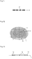
- the wafer 8 is preferably supported horizontally by a support plate 11 as illustrated in figures 12 and 13 , which can be handled manually or by a robot.
- This support plate 11 is in a material compatible with the oxidation treatment, for example quartz, silicon or silicon carbide.
- spacers 12 which support the wafer 8 in zones which do not contain components (in particular between the components).
- Plate 8 is prevented from moving horizontally by retaining elements 13 cooperating with the periphery of plate 8.
- Spacers 12 and retaining elements 13 are generally cylindrical in shape.
- the support plate 11 are integral with the support plate 11, for example fixed to the support plate 11 by bayonet type connections. They are made, for example, of quartz or of silicon carbide, and may be of the same material or of different materials. In a preferred embodiment, the support plate 11 is made of silicon and the spacers and retaining elements 12, 13 are made of quartz. Such a support plate 11 with its spacers 12 and retaining elements 13 can also be used during the step of figure 11 when this consists of a CVD or PVD deposit operation.
- the wafer 8 is placed on the support plate 11 in an upturned position with respect to the oxidation treatment of the figure 7 .
- the wafer 8 is placed on the support plate 11 in an upturned position with respect to the oxidation treatment of the figure 9 .
- the step of releasing the wafer 8 from the substrate 1 can be implemented by eliminating all of the lower layer of silicon 3 and all of the intermediate layer of silicon oxide 4 by chemical etching or plasma etching. It is also possible to remove the lower layer of silicon 3 and the intermediate layer of silicon oxide 4 only on the back of the components or groups of components, the wafer 8 then keeping part of these layers 3, 4. However, these operations are long and costly.
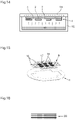
- the wafer 8 is preferably formed by a part of the upper layer of silicon 2 and its release from the substrate 1 is implemented in the manner explained below and illustrated in figures 14 and 15 .
- the etched substrate 1 is fixed as shown in figure 5 against a heating element 14 in a closed chamber 15 ( figure 14 ), the upper layer of silicon 2 being oriented downwards, the lower layer of silicon 3, therefore oriented upwards, being against the heating element 14.
- the method of fixing the substrate 1 against the heating element 14 can be electrostatic (by application of an electric field) or mechanical.
- a hydrofluoric acid (HF) solution is added to chamber 15, out of contact with substrate 1.
- the hydrofluoric acid vapors which then saturate the interior of chamber 15 etch the intermediate layer of silicon oxide 4, without attacking the silicon.
- the heating element 14, regulated in temperature prevents the condensation of the water produced by the reaction between the hydrofluoric acid and the silicon oxide, condensation which would cause sticking between the part to be released and the rest of the substrate 1.
- the part to be released namely the wafer 8 is defined beforehand by a groove made during the etching of the upper layer of silicon 2 and which forms the perimeter of the wafer 8.
- openings 16 for example in the form of hatching as depicted in figure 15 , are engraved in the wafer 8 around a central zone 17 comprising the components. These openings 16 allow the passage of hydrofluoric acid vapor.
- the figure 15 shows an example of plate 8 having a shape consisting of rectangular or square parts. Other shapes can of course be envisaged, for example the circular shape. To the figure 15 one can see the horological components 18 carried by the wafer 8, here made up of hairsprings. These timepiece components have been represented in reduced numbers compared to their real number, in order to facilitate reading of the drawing.
- the horological components manufactured by the process according to the invention can have very precise dimensions and good surface conditions which will improve the operating precision and the efficiency of the mechanisms which will use them.
- the watch components would then have a composite structure comprising one or more intermediate layers of silicon oxide.
- the photosensitive lacquer mask 5 which is used to structure the upper layer of silicon 2 ( figure 3 ) could be replaced by a silicon oxide mask. It would also be possible to combine a mask of photosensitive lacquer and a mask of silicon oxide to produce, by etching in the upper layer of silicon or in a group of upper layers, multilevel timepiece components.
- the substrate could be etched from its two faces.
- the layer or layers of silicon oxides used to stop the etching could be reinforced by one or layers of the parylene type.
- the present invention does not exclude either the use of one or more metal layers to stop the etching.
Landscapes
- Chemical & Material Sciences (AREA)
- Engineering & Computer Science (AREA)
- Metallurgy (AREA)
- Physics & Mathematics (AREA)
- General Physics & Mathematics (AREA)
- Organic Chemistry (AREA)
- Materials Engineering (AREA)
- Manufacturing & Machinery (AREA)
- Chemical Kinetics & Catalysis (AREA)
- Mechanical Engineering (AREA)
- Crystallography & Structural Chemistry (AREA)
- Inorganic Chemistry (AREA)
- General Chemical & Material Sciences (AREA)
- Thermal Sciences (AREA)
- Micromachines (AREA)
- Weting (AREA)
- Crystals, And After-Treatments Of Crystals (AREA)
Claims (17)
- Verfahren zur Herstellung von Uhrenkomponenten, das die folgenden Schritte umfasst:a) Bereitstellen eines Substrats (1), das eine erste Siliziumschicht (2), eine zweite Siliziumschicht (3) und zwischen den beiden eine Siliziumoxid-Zwischenschicht (4) umfasst,b) Ätzen der ersten Siliziumschicht (2), um die Uhrenkomponenten darin zu bilden,c) Befreien eines Plättchens (8), das aus mindestens der gesamten geätzten ersten Siliziumschicht (2) oder einem Teil davon gebildet ist und die Uhrenkomponenten umfasst, von dem Substrat (1),d) thermisches Oxidieren und dann Desoxidieren der Uhrenkomponenten,e) Bilden einer Siliziumoxidschicht (10) auf den Uhrenkomponenten durch thermische Oxidation oder Abscheiden, undf) Lösen der Uhrenkomponenten von dem Plättchen (8).
- Verfahren zur Herstellung von Uhrenkomponenten, das die folgenden Schritte umfasst:a) Bereitstellen eines Substrats (20), das mit Siliziumoxidschichten verschachtelte Siliziumschichten umfasst,b) Ätzen einer Gruppe von Schichten des Substrats, um darin die Uhrenkomponenten zu bilden,c) Befreien eines Plättchens, das aus mindestens der gesamten Gruppe von Schichten oder einem Teil davon gebildet ist und die Uhrenkomponenten umfasst, von dem Substrat,d) thermisches Oxidieren und dann Desoxidieren der Uhrenkomponenten,e) Bilden einer Siliziumoxidschicht auf den Uhrenkomponenten durch thermische Oxidation oder Abscheiden, undf) Lösen der Uhrenkomponenten von dem Plättchen.
- Verfahren nach Anspruch 1 oder 2, wobei das Ätzen im Schritt b) ein reaktives Ionentiefenätzen umfasst.
- Verfahren nach einem der Ansprüche 1 bis 3, das zwischen den Schritten d) und e) einen zusätzlichen Schritt umfasst, der darin besteht, die Uhrenkomponenten thermisch zu oxidieren und dann zu desoxidieren.
- Verfahren nach Anspruch 4, wobei der Schritt d) dazu dient, den Oberflächenzustand der Uhrenkomponenten zu verbessern, und der zusätzliche Schritt dazu dient, die Steifigkeit von Spiralen anzupassen, aus denen die Uhrenkomponenten bestehen.
- Verfahren nach Anspruch 4 oder 5, wobei während des Vorgangs der thermischen Oxidation des zusätzlichen Schritts das Plättchen (8) sich in einer in Bezug auf den Vorgang der thermischen Oxidation des Schritts d) umgedrehten Position befindet.
- Verfahren nach einem der Ansprüche 4 bis 6, wobei während des Schritts e) das Plättchen (8) sich in einer in Bezug auf den Vorgang der thermischen Oxidation des zusätzlichen Schritts umgedrehten Position befindet.
- Verfahren nach einem der Ansprüche 1 bis 7, wobei während des oder den Vorgängen der thermischen Oxidation das Plättchen (8) von einem Stützorgan (11, 12, 13) gestützt wird, das eine Stützplatte (11) und Querstreben (12) und Rückhalteelemente (13) umfasst, die von der Stützplatte (11) getragen werden, wobei die Querstreben (12) einen Abstand zwischen dem Plättchen (8) und der Stützplatte (11) halten, wobei die Rückhalteelemente (13) das Plättchen (8) daran hindern, sich horizontal zu bewegen.
- Verfahren nach Anspruch 8, wobei die Querstreben (12) das Plättchen (8) in Zonen des Plättchens (8) stützen, die keine Uhrenkomponente umfassen.
- Verfahren nach Anspruch 8 oder 9, wobei die Stützplatte (11) aus Silizium, Quarz oder Siliziumcarbid ist.
- Verfahren nach einem der Ansprüche 8 bis 10, wobei die Querstreben (12) und die Rückhalteelemente (13) aus Quarz oder Siliziumcarbid sind.
- Verfahren nach einem der Ansprüche 8 bis 11, wobei die Querstreben (12) und die Rückhalteelemente (13) durch Verbindungen vom Bajonetttyp an der Stützplatte (11) befestigt sind.
- Verfahren nach einem der Ansprüche 1 und 3 bis 12, wobei der Schritt c) einen Vorgang des Gasphasenätzens der Siliziumoxid-Zwischenschicht (4) umfasst.
- Verfahren nach einem der Ansprüche 1 und 3 bis 13, wobei das im Schritt c) befreite Plättchen (8) aus einem Teil der geätzten ersten Siliziumschicht (2) gebildet wird.
- Verfahren nach einem der Ansprüche 1 und 3 bis 14, wobei im Schritt b) eine Einkerbung in die erste Siliziumschicht (2) geätzt wird, um den Umfang des im Schritt c) zu befreienden Plättchens (8) zu definieren.
- Verfahren nach einem der Ansprüche 1 und 3 bis 15, wobei im Schritt b) Öffnungen (16) in die erste Siliziumschicht (2) um eine zentrale Zone (17) geätzt werden, wo die Uhrenkomponenten (18) geätzt werden, wobei diese Öffnungen (16) während des Schritts c) den Durchgang eines Ätzmittels zum Ätzen der Siliziumoxid-Zwischenschicht (4) ermöglichen.
- Verfahren nach einem der Ansprüche 1 bis 16, wobei die Uhrenkomponenten mindestens einen von den folgenden Komponententypen umfassen: Spiralen (18), Anker, Räder, Zeiger, Wippen, Hebel, Federn, Unruhen oder Teile solcher Komponenten.
Priority Applications (2)
| Application Number | Priority Date | Filing Date | Title |
|---|---|---|---|
| EP21182494.1A EP3907567B1 (de) | 2018-03-20 | 2019-03-19 | Trägerelement für die wärmebehandlung eines plättchens |
| EP24216887.0A EP4492160B1 (de) | 2018-03-20 | 2019-03-19 | Trägerorgan zur wärmebehandlung eines wafers |
Applications Claiming Priority (2)
| Application Number | Priority Date | Filing Date | Title |
|---|---|---|---|
| EP18162729.0A EP3543795A1 (de) | 2018-03-20 | 2018-03-20 | Herstellungsverfahren von uhrkomponenten aus silizium |
| PCT/IB2019/052198 WO2019180596A1 (fr) | 2018-03-20 | 2019-03-19 | Procede de fabrication de composants horlogers en silicium |
Related Child Applications (3)
| Application Number | Title | Priority Date | Filing Date |
|---|---|---|---|
| EP24216887.0A Division EP4492160B1 (de) | 2018-03-20 | 2019-03-19 | Trägerorgan zur wärmebehandlung eines wafers |
| EP21182494.1A Division EP3907567B1 (de) | 2018-03-20 | 2019-03-19 | Trägerelement für die wärmebehandlung eines plättchens |
| EP21182494.1A Division-Into EP3907567B1 (de) | 2018-03-20 | 2019-03-19 | Trägerelement für die wärmebehandlung eines plättchens |
Publications (2)
| Publication Number | Publication Date |
|---|---|
| EP3769162A1 EP3769162A1 (de) | 2021-01-27 |
| EP3769162B1 true EP3769162B1 (de) | 2022-08-10 |
Family
ID=61691846
Family Applications (4)
| Application Number | Title | Priority Date | Filing Date |
|---|---|---|---|
| EP18162729.0A Withdrawn EP3543795A1 (de) | 2018-03-20 | 2018-03-20 | Herstellungsverfahren von uhrkomponenten aus silizium |
| EP21182494.1A Active EP3907567B1 (de) | 2018-03-20 | 2019-03-19 | Trägerelement für die wärmebehandlung eines plättchens |
| EP24216887.0A Active EP4492160B1 (de) | 2018-03-20 | 2019-03-19 | Trägerorgan zur wärmebehandlung eines wafers |
| EP19717200.0A Active EP3769162B1 (de) | 2018-03-20 | 2019-03-19 | Herstellungsverfahren von uhrkomponenten aus silizium |
Family Applications Before (3)
| Application Number | Title | Priority Date | Filing Date |
|---|---|---|---|
| EP18162729.0A Withdrawn EP3543795A1 (de) | 2018-03-20 | 2018-03-20 | Herstellungsverfahren von uhrkomponenten aus silizium |
| EP21182494.1A Active EP3907567B1 (de) | 2018-03-20 | 2019-03-19 | Trägerelement für die wärmebehandlung eines plättchens |
| EP24216887.0A Active EP4492160B1 (de) | 2018-03-20 | 2019-03-19 | Trägerorgan zur wärmebehandlung eines wafers |
Country Status (5)
| Country | Link |
|---|---|
| US (2) | US11880165B2 (de) |
| EP (4) | EP3543795A1 (de) |
| JP (2) | JP2021518548A (de) |
| CN (2) | CN111868637B (de) |
| WO (1) | WO2019180596A1 (de) |
Families Citing this family (22)
| Publication number | Priority date | Publication date | Assignee | Title |
|---|---|---|---|---|
| EP3543796A1 (de) * | 2018-03-21 | 2019-09-25 | Nivarox-FAR S.A. | Verfahren zur herstellung einer siliziumfeder |
| EP3839642A1 (de) | 2019-12-20 | 2021-06-23 | Patek Philippe SA Genève | Herstellungsverfahren von uhrenfedern und ätzmaske für ein solches verfahren |
| EP3865954B1 (de) * | 2020-02-12 | 2025-08-13 | Nivarox-FAR S.A. | Herstellungsverfahren einer monoblock-vorrichtung mit federzungen aus silizium, für uhrwerk |
| EP3882714A1 (de) * | 2020-03-19 | 2021-09-22 | Patek Philippe SA Genève | Verfahren zur herstellung einer uhrenkomponente aus silizium |
| EP3882710A1 (de) * | 2020-03-19 | 2021-09-22 | Patek Philippe SA Genève | Verfahren zur herstellung einer uhrenkomponente auf siliziumbasis |
| EP3907565A1 (de) | 2020-05-07 | 2021-11-10 | Patek Philippe SA Genève | Verfahren zur herstellung einer uhrenkomponente aus silizium |
| NL2028796B1 (en) * | 2021-07-20 | 2023-01-23 | Flexous Mech Ip B V | Method of manufacturing a plurality of mechanical resonators in a manufacturing wafer |
| EP4177940A1 (de) * | 2021-11-03 | 2023-05-10 | Nexperia B.V. | Halbleiterbauelement-anordnung sowie verfahren zur herstellung einer solchen halbleiterbauelement-anordnung |
| EP4212965A1 (de) | 2022-01-14 | 2023-07-19 | Richemont International S.A. | Verfahren zur begrenzung der verformung einer uhrenkomponente aus silizium |
| EP4227742B1 (de) | 2022-02-11 | 2024-11-13 | Sigatec SA | Verfahren zur herstellung eines siliziumbauteils |
| EP4312084B1 (de) | 2022-07-26 | 2026-06-24 | Nivarox-FAR S.A. | Verfahren zur herstellung einer siliziumspirale |
| CH720935A1 (fr) | 2023-07-11 | 2025-01-15 | Richemont Int Sa | Procédé de fabrication de composants horlogers en silicium sur une plaquette SOI |
| CH721138A1 (fr) | 2023-09-20 | 2025-03-31 | Richemont Int Sa | Procédé de fabrication de composants horlogers en silicium |
| CH721146A1 (fr) | 2023-09-21 | 2025-03-31 | Richemont Int Sa | Procédé de fabrication de composants horlogers en silicium |
| EP4553586A1 (de) | 2023-11-08 | 2025-05-14 | Patek Philippe SA Genève | Verfahren zur herstellung einer rückstellfeder mit genauer steifigkeit für einen uhrresonator |
| EP4567527A1 (de) | 2023-12-06 | 2025-06-11 | Richemont International S.A. | Verfahren zur herstellung von uhrenkomponenten aus silizium |
| EP4625064A1 (de) | 2024-03-27 | 2025-10-01 | Richemont International S.A. | Verfahren zur herstellung von uhrenkomponenten aus silizium |
| EP4730048A1 (de) | 2024-10-18 | 2026-04-22 | Richemont International S.A. | Verfahren zur herstellung von uhrenkomponenten aus silizium auf einer einzelnen siliziumscheibe ohne trägerschicht. |
| EP4730049A1 (de) | 2024-10-18 | 2026-04-22 | Richemont International S.A. | Verfahren zur herstellung von uhrenkomponenten aus silizium |
| EP4741946A1 (de) | 2024-10-18 | 2026-05-13 | Richemont International SA | Verfahren zur herstellung von uhrenkomponenten aus silizium |
| EP4738019A1 (de) | 2024-10-31 | 2026-05-06 | Richemont International S.A. | Verfahren zur herstellung von uhrenkomponenten |
| EP4752645A1 (de) * | 2024-11-28 | 2026-06-03 | Richemont International S.A. | Verfahren zur herstellung von unruhfedern auf einem träger |
Citations (20)
| Publication number | Priority date | Publication date | Assignee | Title |
|---|---|---|---|---|
| US4400861A (en) | 1981-11-27 | 1983-08-30 | Oyo Instruments, Inc. | Fabrication of seismic springs from sheets |
| EP0732635A1 (de) | 1995-03-17 | 1996-09-18 | C.S.E.M. Centre Suisse D'electronique Et De Microtechnique Sa | Mikromechanischer Teil und Verfahren zur dessen Herstellung |
| US6192603B1 (en) | 1998-08-26 | 2001-02-27 | Sony Corporation | Vacuum processing apparatus and magnetic seal rotary bearing unit |
| EP1422436A1 (de) | 2002-11-25 | 2004-05-26 | CSEM Centre Suisse d'Electronique et de Microtechnique SA | Spiraluhrwerkfeder und Verfahren zu deren Herstellung |
| SG112005A1 (en) | 2003-12-29 | 2005-06-29 | Sony Corp | A surface treatment for use in the fabrication of mems devices |
| WO2007000271A1 (fr) | 2005-06-28 | 2007-01-04 | Eta Sa Manufacture Horlogere Suisse | Piece de micro-mecanique renforcee |
| US20070026614A1 (en) | 2005-07-27 | 2007-02-01 | The Regents Of The University Of California | CMOS-compatible high-performance microscanners, including structures, high-yield simplified fabrication methods and applications |
| WO2009068091A1 (fr) | 2007-11-28 | 2009-06-04 | Manufacture Et Fabrique De Montres Et Chronomètres Ulysse Nardin Le Locle S.A. | Oscillateur mécanique présentant un coefficient thermoélastique optimisé |
| WO2010057777A1 (fr) | 2008-11-21 | 2010-05-27 | Nivarox-Far S.A. | Procédé de fabrication d'une pièce de micromécanique |
| CH703051A2 (de) | 2010-04-21 | 2011-10-31 | Team Smartfish Gmbh | Spiralfeder für ein Uhrwerk und entsprechendes Herstellungsverfahren. |
| JP2014168819A (ja) | 2013-03-01 | 2014-09-18 | Nippon Telegr & Teleph Corp <Ntt> | マイクロメカニカル構造体の作製方法 |
| EP2799939A1 (de) | 2013-04-30 | 2014-11-05 | Universo S.A. | Träger für die Behandlung von mikromechanischen Bauteilen |
| WO2015113973A1 (fr) | 2014-01-29 | 2015-08-06 | Cartier Création Studio Sa | Ressort spiral thermocompensé en céramique comprenant l' élément silicium dans sa composition et son procédé de réglage |
| JP2015179067A (ja) | 2014-02-26 | 2015-10-08 | シチズンホールディングス株式会社 | ひげぜんまいの製造方法 |
| EP2937311A1 (de) | 2014-04-25 | 2015-10-28 | Rolex Sa | Herstellungsverfahren einer verstärkten uhrkomponente, entsprechende uhrkomponente und entsprechende uhr |
| WO2016128694A1 (fr) | 2015-02-13 | 2016-08-18 | Tronic's Microsystems | Oscillateur mécanique et procédé de réalisation associe |
| JP2016161394A (ja) | 2015-03-02 | 2016-09-05 | シチズンホールディングス株式会社 | 時計部品 |
| JP2016173356A (ja) | 2015-03-16 | 2016-09-29 | シチズンホールディングス株式会社 | シリコン製機械部品の製造方法 |
| US20170115063A1 (en) | 2015-10-26 | 2017-04-27 | Sunedison Semiconductor Limited (Uen201334164H) | Semiconductor wafer support ring for heat treatment |
| EP3181938A1 (de) | 2015-12-18 | 2017-06-21 | CSEM Centre Suisse d'Electronique et de Microtechnique SA - Recherche et Développement | Herstellungsverfahren einer spiralfeder mit einer vorbestimmten steifigkeit durch wegnahme von material |
Family Cites Families (37)
| Publication number | Priority date | Publication date | Assignee | Title |
|---|---|---|---|---|
| US6706202B1 (en) * | 2000-09-28 | 2004-03-16 | Xerox Corporation | Method for shaped optical MEMS components with stressed thin films |
| JP2002341054A (ja) * | 2001-05-11 | 2002-11-27 | Seiko Instruments Inc | ヒゲぜんまい、同構造体、これを用いた調速機構及び時計 |
| TW504460B (en) * | 2001-05-25 | 2002-10-01 | Benq Corp | Chip protection device |
| US20040255442A1 (en) * | 2003-06-19 | 2004-12-23 | Mcdiarmid James | Methods and apparatus for processing workpieces |
| TWI258208B (en) * | 2004-01-14 | 2006-07-11 | Mosel Vitelic Inc | Loading device for wafer and the supporting structure thereof |
| JP2006032716A (ja) * | 2004-07-16 | 2006-02-02 | Topcon Corp | メンブレンチップ製造方法 |
| KR20070091332A (ko) * | 2005-01-18 | 2007-09-10 | 에이에스엠 아메리카, 인코포레이티드 | 웨이퍼 지지핀 어셈블리 |
| JP2007130864A (ja) * | 2005-11-10 | 2007-05-31 | Seiko Epson Corp | ウェハ固定治具、ノズル基板の製造方法並びに液滴吐出ヘッドの製造方法 |
| US7998308B2 (en) * | 2006-04-18 | 2011-08-16 | Tokyo Electron Limited | Liquid processing apparatus |
| US8614110B1 (en) * | 2006-07-25 | 2013-12-24 | The United States Of America As Represented By The Secretary Of The Navy | Method for fabricating a dual-crystalline silicon suspension system using pre-fabricated cavities |
| KR100849366B1 (ko) * | 2006-08-24 | 2008-07-31 | 세메스 주식회사 | 기판을 처리하는 장치 및 방법 |
| CH714952B1 (fr) * | 2007-05-08 | 2019-10-31 | Patek Philippe Sa Geneve | Composant horloger, son procédé de fabrication et application de ce procédé. |
| JP5276420B2 (ja) * | 2008-01-31 | 2013-08-28 | 大日本スクリーン製造株式会社 | 基板処理装置および基板処理方法 |
| US8030133B2 (en) * | 2008-03-28 | 2011-10-04 | Icemos Technology Ltd. | Method of fabricating a bonded wafer substrate for use in MEMS structures |
| JP2010110877A (ja) * | 2008-11-10 | 2010-05-20 | Toyota Motor Corp | 電子装置、及び電子装置の製造方法 |
| KR101017654B1 (ko) * | 2008-11-26 | 2011-02-25 | 세메스 주식회사 | 기판 척킹 부재, 이를 갖는 기판 처리 장치 및 이를 이용한기판 처리 방법 |
| WO2010093568A2 (en) * | 2009-02-11 | 2010-08-19 | Applied Materials, Inc. | Non-contact substrate processing |
| CH701499B1 (fr) | 2009-07-23 | 2016-09-15 | Montres Breguet Sa | Procède de fabrication d'une pièce micromécanique en silicium renforcé. |
| EP2423764B1 (de) | 2010-08-31 | 2013-03-27 | Rolex S.A. | Vorrichtung zum Messen des Drehmomentes einer Spirale |
| EP2437126B1 (de) * | 2010-10-04 | 2019-03-27 | Rolex Sa | Regulierorgan mit Spiralunruh |
| US8222084B2 (en) * | 2010-12-08 | 2012-07-17 | Skorpios Technologies, Inc. | Method and system for template assisted wafer bonding |
| EP2472340B1 (de) | 2011-01-03 | 2021-03-03 | Patek Philippe SA Genève | Bestandteil einer Uhr und sein Herstellungsverfahren |
| US9411314B2 (en) * | 2011-09-29 | 2016-08-09 | Rolex Sa | Integral assembly of a hairspring and a collet |
| US9034754B2 (en) * | 2012-05-25 | 2015-05-19 | LuxVue Technology Corporation | Method of forming a micro device transfer head with silicon electrode |
| CH707797A1 (fr) * | 2013-03-28 | 2014-09-30 | Silicior Sa | Procédé de fabrication d'une pièce micro-mécanique essentiellement plane, et pièce micro-mécanique comportant au moins une portion formée d'oxyde de silicium. |
| EP2799940B1 (de) * | 2013-04-30 | 2019-07-17 | The Swatch Group Management Services AG | Verpackung für Zeiger von Armbanduhren |
| EP3069377A4 (de) * | 2013-11-13 | 2017-05-31 | Michigan Technological University | Siliciumnanodrahtbasierte sensorarrays |
| JP2015179013A (ja) * | 2014-03-19 | 2015-10-08 | シチズンホールディングス株式会社 | ひげぜんまいの製造方法 |
| JP2016133495A (ja) * | 2015-01-22 | 2016-07-25 | シチズンホールディングス株式会社 | 時計部品の製造方法および時計部品 |
| JP6554328B2 (ja) * | 2015-05-29 | 2019-07-31 | 株式会社Screenホールディングス | 熱処理装置 |
| EP3109199B1 (de) * | 2015-06-25 | 2022-05-11 | Nivarox-FAR S.A. | Werkstück auf siliziumbasis mit mindestens einer fase, und sein herstellungsverfahren |
| EP3109200B1 (de) * | 2015-06-25 | 2023-06-28 | Nivarox-FAR S.A. | Mikromechanisches teil mit verkleinerter kontaktfläche, und sein herstellungsverfahren |
| EP3088969B1 (de) * | 2016-03-17 | 2018-12-26 | Sigatec SA | Thermocompensierte spiralfeder und verfahren zu deren herstellung |
| JP6653608B2 (ja) * | 2016-03-29 | 2020-02-26 | 株式会社Screenホールディングス | 基板処理装置および基板処理方法 |
| JP2019519914A (ja) * | 2016-05-11 | 2019-07-11 | スコーピオズ テクノロジーズ インコーポレイテッド | シリコンフォトニクスにおけるiii−vチップの作成および集積化 |
| JP6770886B2 (ja) * | 2016-12-28 | 2020-10-21 | 株式会社Screenホールディングス | 基板処理装置及び基板処理方法 |
| TWI796444B (zh) | 2018-03-20 | 2023-03-21 | 瑞士商百達翡麗日內瓦股份有限公司 | 用於製造精確剛度之時計熱補償游絲的方法 |
-
2018
- 2018-03-20 EP EP18162729.0A patent/EP3543795A1/de not_active Withdrawn
-
2019
- 2019-03-19 WO PCT/IB2019/052198 patent/WO2019180596A1/fr not_active Ceased
- 2019-03-19 US US16/980,126 patent/US11880165B2/en active Active
- 2019-03-19 JP JP2020550771A patent/JP2021518548A/ja active Pending
- 2019-03-19 EP EP21182494.1A patent/EP3907567B1/de active Active
- 2019-03-19 CN CN201980020156.7A patent/CN111868637B/zh active Active
- 2019-03-19 EP EP24216887.0A patent/EP4492160B1/de active Active
- 2019-03-19 CN CN202210052591.1A patent/CN114460826B/zh active Active
- 2019-03-19 EP EP19717200.0A patent/EP3769162B1/de active Active
-
2023
- 2023-09-11 JP JP2023146855A patent/JP7769670B2/ja active Active
- 2023-12-08 US US18/533,303 patent/US20240103442A1/en active Pending
Patent Citations (21)
| Publication number | Priority date | Publication date | Assignee | Title |
|---|---|---|---|---|
| US4400861A (en) | 1981-11-27 | 1983-08-30 | Oyo Instruments, Inc. | Fabrication of seismic springs from sheets |
| EP0732635A1 (de) | 1995-03-17 | 1996-09-18 | C.S.E.M. Centre Suisse D'electronique Et De Microtechnique Sa | Mikromechanischer Teil und Verfahren zur dessen Herstellung |
| US6192603B1 (en) | 1998-08-26 | 2001-02-27 | Sony Corporation | Vacuum processing apparatus and magnetic seal rotary bearing unit |
| EP1422436A1 (de) | 2002-11-25 | 2004-05-26 | CSEM Centre Suisse d'Electronique et de Microtechnique SA | Spiraluhrwerkfeder und Verfahren zu deren Herstellung |
| SG112005A1 (en) | 2003-12-29 | 2005-06-29 | Sony Corp | A surface treatment for use in the fabrication of mems devices |
| WO2007000271A1 (fr) | 2005-06-28 | 2007-01-04 | Eta Sa Manufacture Horlogere Suisse | Piece de micro-mecanique renforcee |
| US20070026614A1 (en) | 2005-07-27 | 2007-02-01 | The Regents Of The University Of California | CMOS-compatible high-performance microscanners, including structures, high-yield simplified fabrication methods and applications |
| WO2009068091A1 (fr) | 2007-11-28 | 2009-06-04 | Manufacture Et Fabrique De Montres Et Chronomètres Ulysse Nardin Le Locle S.A. | Oscillateur mécanique présentant un coefficient thermoélastique optimisé |
| WO2010057777A1 (fr) | 2008-11-21 | 2010-05-27 | Nivarox-Far S.A. | Procédé de fabrication d'une pièce de micromécanique |
| CH703051A2 (de) | 2010-04-21 | 2011-10-31 | Team Smartfish Gmbh | Spiralfeder für ein Uhrwerk und entsprechendes Herstellungsverfahren. |
| JP2014168819A (ja) | 2013-03-01 | 2014-09-18 | Nippon Telegr & Teleph Corp <Ntt> | マイクロメカニカル構造体の作製方法 |
| EP2799939A1 (de) | 2013-04-30 | 2014-11-05 | Universo S.A. | Träger für die Behandlung von mikromechanischen Bauteilen |
| WO2015113973A1 (fr) | 2014-01-29 | 2015-08-06 | Cartier Création Studio Sa | Ressort spiral thermocompensé en céramique comprenant l' élément silicium dans sa composition et son procédé de réglage |
| JP2015179067A (ja) | 2014-02-26 | 2015-10-08 | シチズンホールディングス株式会社 | ひげぜんまいの製造方法 |
| EP2937311A1 (de) | 2014-04-25 | 2015-10-28 | Rolex Sa | Herstellungsverfahren einer verstärkten uhrkomponente, entsprechende uhrkomponente und entsprechende uhr |
| WO2016128694A1 (fr) | 2015-02-13 | 2016-08-18 | Tronic's Microsystems | Oscillateur mécanique et procédé de réalisation associe |
| JP2016161394A (ja) | 2015-03-02 | 2016-09-05 | シチズンホールディングス株式会社 | 時計部品 |
| JP2016173356A (ja) | 2015-03-16 | 2016-09-29 | シチズンホールディングス株式会社 | シリコン製機械部品の製造方法 |
| JP2016173355A (ja) | 2015-03-16 | 2016-09-29 | シチズンホールディングス株式会社 | 機械部品の製造方法 |
| US20170115063A1 (en) | 2015-10-26 | 2017-04-27 | Sunedison Semiconductor Limited (Uen201334164H) | Semiconductor wafer support ring for heat treatment |
| EP3181938A1 (de) | 2015-12-18 | 2017-06-21 | CSEM Centre Suisse d'Electronique et de Microtechnique SA - Recherche et Développement | Herstellungsverfahren einer spiralfeder mit einer vorbestimmten steifigkeit durch wegnahme von material |
Non-Patent Citations (17)
| Title |
|---|
| "Académie francaises", 31 December 2022, ACADÉMIE FRANCAISES, article ANONYMOUS: "Horloger, Horlogère", XP093108244 |
| "ACADÉMIE FRANCAISES:", 31 December 2022, ACADÉMIE FRANCAISES, article ANONYMOUS: "Horlogerie", XP093108240 |
| ANONYMOUS: " HF VAPOR ETCHER - HFVE STANDARD", A.M.M.T., 12 February 2016 (2016-02-12), XP093157640, Retrieved from the Internet <URL:https://www.ammt.com/support/files/AMMT_PI_HFVEStandard.pdf> |
| ANONYMOUS: "Microsystème électromécanique", WIKIPÉDIA, L'ENCYCLOPÉDIE LIBRE, 27 April 2023 (2023-04-27), XP093108246, Retrieved from the Internet <URL:https://fr.wikipedia.org/wiki/Microsyst%C3%A8me_%C3%A9lectrom%C3%A9canique> [retrieved on 20231204] |
| ANONYMOUS: "Qualcomm Toq smart watch to go for sale on Dec.2, but with an entry price of US$349.99, is still expensive luxury", 19 November 2013 (2013-11-19), XP093157650, Retrieved from the Internet <URL:https://english.etnews.com/20131119200007> |
| ANONYMOUS: "Silicon on insulator", WIKIPEDIA, 16 November 2018 (2018-11-16), pages 1 - 6, XP093217528, Retrieved from the Internet <URL:https://en.wikipedia.org/w/index.php?title=Silicon_on_insulator&oldid=869160080> |
| G.V. HERRERA ; T. BAUER ; M.G. BLAIN ; P.E. DODD ; R. DONDERO ; E.J. GARCIA ; P.C. GALAMBOS ; D.L. HETHERINGTON ; J.J. HUDGENS ; F: "SOI-enabled MEMS processes lead to novel mechanical, optical, and atomic physics devices", 2008 IEEE INTERNATIONAL SOI CONFERENCE PROCEEDINGS, 6 October 2008 (2008-10-06), Piscataway, NJ, USA , pages 5 - 8, XP031351829, ISBN: 978-1-4244-1954-8 |
| HERRERA, G.V. ET AL.: "SOI-Enabled MEMS Processes Lead to Novel Mechanical, Optical and Atomic Physics Devices", 2008 IEEE INTERNATIONAL SOI CONFÉRENCE PROCEEDINGS, 2008, pages 5 - 8, XP031351829 |
| LAURA MCCREDDIE-DOAK: "This is where Patek Philippe develops the watches of the future | WIRED UK", 31 December 2017 (2017-12-31), XP055699852, Retrieved from the Internet <URL:https://www.wired.co.uk/article/patek-philippes-aquanaut-travel-time-is-packed-with-innovation> [retrieved on 20200529] |
| NOELL W., CLERC P.-A., JEANNERET S., HOOGERWERF A., NIEDERMANN P., PERRET A., DE ROOIJ N.F.: "MEMS for a watches", MICRO ELECTRO MECHANICAL SYSTEMS, 2004. 17TH IEEE INTERNATIONAL CONFER ENCE ON. (MEMS) MAASTRICHT, NETHERLANDS 25-29 JAN. 2004, PISCATAWAY, NJ, USA,IEEE, US, 25 January 2004 (2004-01-25) - 29 January 2004 (2004-01-29), US , pages 1 - 4, XP010767811, ISBN: 978-0-7803-8265-7, DOI: 10.1109/MEMS.2004.1290507 |
| P. CLARKE: "MEMS scanner projects Bosch Sensortec into displays, user interfaces", EENEWS ANALOG, 27 February 2017 (2017-02-27), XP093157648 |
| SARI, I. ET AL.: "A Full Wafer Dicing Free Dry Release Process For MEMS Devices", PROC. EUROSENSORS XXIV, PROCEDIA ENGINEERING, vol. 5, 2010, pages 850 - 853, XP027483798, DOI: 10.1016/j.proeng.2010.09.242 |
| SIDEWALL SMOOTHING OF BOSCH SCALLOPS VIA THERMAL OXIDATION, 7 June 2012 (2012-06-07), XP055699858, Retrieved from the Internet <URL:https://www.nanofab.ualberta.ca/wp- content/uploads/downloads/2012/06/Sidewall-smoothing-using- thermal-oxidation-steps 2.pd> |
| SYLVAIN AUBRY: "Théorie des échappements", 1 July 2016, FÉDÉRATION DES ÉCOLES TECHNIQUES, FR, ISBN: 2940025517, article SYLVAIN AUBRY: "5.2 Gravure profonde du silicium (DRIE)", pages: 287 - 292, 368, XP009563799 |
| T M FAHIM AMIN: "Design and Fabrication of Micro-electro-mechanical Systems Actuators for Application in External Cavity Tunable Lasers", DOCTORAL THESIS, UNIVERSITY OF ALBERTA, 1 January 2014 (2014-01-01), XP093157631 |
| ZISHAN ALI SYED MOHAMMED, M.A.S. OLIMPOA , D.P. POENARA , S. ADITYA: "Smoothening of scalloped DRIE trench walls", MATERIALS SCIENCE IN SEMICONDUCTOR PROCESSING., ELSEVIER SCIENCE PUBLISHERS B.V., BARKING., UK, vol. 63, 1 June 2017 (2017-06-01), UK , pages 83 - 89, XP093157619, ISSN: 1369-8001, DOI: 10.1016/j.mssp.2017.02.006 |
| ZUJUN SHI, SHIQIAN SHAO, YI WANG: "Improved the Surface Roughness of Silicon Nanophotonic Devices by Thermal Oxidation Method", JOURNAL OF PHYSICS: CONFERENCE SERIES, INSTITUTE OF PHYSICS PUBLISHING, BRISTOL, GB, vol. 276, 1 February 2011 (2011-02-01), GB , pages 012087, XP093157636, ISSN: 1742-6596, DOI: 10.1088/1742-6596/276/1/012087 |
Also Published As
| Publication number | Publication date |
|---|---|
| EP3769162A1 (de) | 2021-01-27 |
| CN111868637B (zh) | 2022-04-12 |
| EP3907567A1 (de) | 2021-11-10 |
| JP2021518548A (ja) | 2021-08-02 |
| EP4492160A3 (de) | 2025-04-30 |
| CN114460826A (zh) | 2022-05-10 |
| EP3907567B1 (de) | 2025-01-08 |
| EP4492160A2 (de) | 2025-01-15 |
| US11880165B2 (en) | 2024-01-23 |
| US20240103442A1 (en) | 2024-03-28 |
| US20210026299A1 (en) | 2021-01-28 |
| EP4492160B1 (de) | 2026-04-08 |
| JP7769670B2 (ja) | 2025-11-13 |
| CN111868637A (zh) | 2020-10-30 |
| WO2019180596A1 (fr) | 2019-09-26 |
| CN114460826B (zh) | 2024-07-09 |
| JP2023164549A (ja) | 2023-11-10 |
| EP3543795A1 (de) | 2019-09-25 |
Similar Documents
| Publication | Publication Date | Title |
|---|---|---|
| EP3907567B1 (de) | Trägerelement für die wärmebehandlung eines plättchens | |
| EP3769161B1 (de) | Herstellungsverfahren von thermokompensierten spiralen mit exakter steifigkeit | |
| EP3769160A1 (de) | Verfahren zur herstellung einer siliciumhaarfeder | |
| EP3181938B1 (de) | Herstellungsverfahren einer spiralfeder mit einer vorbestimmten steifigkeit durch wegnahme von material | |
| EP3495894B1 (de) | Verfahren zur herstellung einer uhrkomponente | |
| EP3181939B1 (de) | Herstellungsverfahren einer spiralfeder mit einer vorbestimmten steifigkeit durch zugabe von material | |
| JP2023164549A5 (de) | ||
| EP3181940B1 (de) | Herstellungsverfahren einer spiralfeder mit einer vorbestimmten steifigkeit durch lokalisierte wegnahme von material | |
| CH714806B1 (fr) | Procédé de fabrication de composants horlogers en silicium. | |
| EP3865954B1 (de) | Herstellungsverfahren einer monoblock-vorrichtung mit federzungen aus silizium, für uhrwerk | |
| EP4111264A1 (de) | Bauteil aus silizium für eine uhr | |
| CH714815A2 (fr) | Procédé de fabrication d’un spiral en silicium pour l’horlogerie. | |
| EP4052098B1 (de) | Verfahren zur herstellung einer uhrenkomponente aus silizium | |
| CH717124A2 (fr) | Procédé de fabrication d'un dispositif à lames flexibles monobloc en silicium, notamment pour l'horlogerie. | |
| EP4553586A1 (de) | Verfahren zur herstellung einer rückstellfeder mit genauer steifigkeit für einen uhrresonator | |
| EP4738020A1 (de) | Verfahren zur herstellung von siliziumbauteilen | |
| EP4738021A1 (de) | Verfahren zur herstellung von siliziumbauteilen | |
| EP4567527A1 (de) | Verfahren zur herstellung von uhrenkomponenten aus silizium | |
| HK40038550A (en) | Method for manufacturing a silicon hairspring | |
| CH718082A2 (fr) | Procédé de fabrication d'un élément élastique pour un système micromécanique. | |
| TW202035890A (zh) | 矽游絲的製造方法 | |
| CH711960B1 (fr) | Procédé de fabrication d'un spiral d'une raideur prédéterminée avec retrait de matière. |
Legal Events
| Date | Code | Title | Description |
|---|---|---|---|
| STAA | Information on the status of an ep patent application or granted ep patent |
Free format text: STATUS: UNKNOWN |
|
| STAA | Information on the status of an ep patent application or granted ep patent |
Free format text: STATUS: THE INTERNATIONAL PUBLICATION HAS BEEN MADE |
|
| TPAC | Observations filed by third parties |
Free format text: ORIGINAL CODE: EPIDOSNTIPA |
|
| PUAI | Public reference made under article 153(3) epc to a published international application that has entered the european phase |
Free format text: ORIGINAL CODE: 0009012 |
|
| STAA | Information on the status of an ep patent application or granted ep patent |
Free format text: STATUS: REQUEST FOR EXAMINATION WAS MADE |
|
| 17P | Request for examination filed |
Effective date: 20200907 |
|
| AK | Designated contracting states |
Kind code of ref document: A1 Designated state(s): AL AT BE BG CH CY CZ DE DK EE ES FI FR GB GR HR HU IE IS IT LI LT LU LV MC MK MT NL NO PL PT RO RS SE SI SK SM TR |
|
| AX | Request for extension of the european patent |
Extension state: BA ME |
|
| DAV | Request for validation of the european patent (deleted) | ||
| DAX | Request for extension of the european patent (deleted) | ||
| TPAA | Information related to observations by third parties modified |
Free format text: ORIGINAL CODE: EPIDOSCTIPA |
|
| GRAP | Despatch of communication of intention to grant a patent |
Free format text: ORIGINAL CODE: EPIDOSNIGR1 |
|
| STAA | Information on the status of an ep patent application or granted ep patent |
Free format text: STATUS: GRANT OF PATENT IS INTENDED |
|
| INTG | Intention to grant announced |
Effective date: 20220422 |
|
| GRAS | Grant fee paid |
Free format text: ORIGINAL CODE: EPIDOSNIGR3 |
|
| GRAA | (expected) grant |
Free format text: ORIGINAL CODE: 0009210 |
|
| STAA | Information on the status of an ep patent application or granted ep patent |
Free format text: STATUS: THE PATENT HAS BEEN GRANTED |
|
| AK | Designated contracting states |
Kind code of ref document: B1 Designated state(s): AL AT BE BG CH CY CZ DE DK EE ES FI FR GB GR HR HU IE IS IT LI LT LU LV MC MK MT NL NO PL PT RO RS SE SI SK SM TR |
|
| REG | Reference to a national code |
Ref country code: AT Ref legal event code: REF Ref document number: 1511003 Country of ref document: AT Kind code of ref document: T Effective date: 20220815 Ref country code: CH Ref legal event code: EP |
|
| REG | Reference to a national code |
Ref country code: IE Ref legal event code: FG4D Free format text: LANGUAGE OF EP DOCUMENT: FRENCH |
|
| REG | Reference to a national code |
Ref country code: DE Ref legal event code: R096 Ref document number: 602019018114 Country of ref document: DE |
|
| REG | Reference to a national code |
Ref country code: NL Ref legal event code: MP Effective date: 20220810 |
|
| REG | Reference to a national code |
Ref country code: LT Ref legal event code: MG9D |
|
| PG25 | Lapsed in a contracting state [announced via postgrant information from national office to epo] |
Ref country code: SE Free format text: LAPSE BECAUSE OF FAILURE TO SUBMIT A TRANSLATION OF THE DESCRIPTION OR TO PAY THE FEE WITHIN THE PRESCRIBED TIME-LIMIT Effective date: 20220810 Ref country code: RS Free format text: LAPSE BECAUSE OF FAILURE TO SUBMIT A TRANSLATION OF THE DESCRIPTION OR TO PAY THE FEE WITHIN THE PRESCRIBED TIME-LIMIT Effective date: 20220810 Ref country code: PT Free format text: LAPSE BECAUSE OF FAILURE TO SUBMIT A TRANSLATION OF THE DESCRIPTION OR TO PAY THE FEE WITHIN THE PRESCRIBED TIME-LIMIT Effective date: 20221212 Ref country code: NO Free format text: LAPSE BECAUSE OF FAILURE TO SUBMIT A TRANSLATION OF THE DESCRIPTION OR TO PAY THE FEE WITHIN THE PRESCRIBED TIME-LIMIT Effective date: 20221110 Ref country code: NL Free format text: LAPSE BECAUSE OF FAILURE TO SUBMIT A TRANSLATION OF THE DESCRIPTION OR TO PAY THE FEE WITHIN THE PRESCRIBED TIME-LIMIT Effective date: 20220810 Ref country code: LV Free format text: LAPSE BECAUSE OF FAILURE TO SUBMIT A TRANSLATION OF THE DESCRIPTION OR TO PAY THE FEE WITHIN THE PRESCRIBED TIME-LIMIT Effective date: 20220810 Ref country code: LT Free format text: LAPSE BECAUSE OF FAILURE TO SUBMIT A TRANSLATION OF THE DESCRIPTION OR TO PAY THE FEE WITHIN THE PRESCRIBED TIME-LIMIT Effective date: 20220810 Ref country code: FI Free format text: LAPSE BECAUSE OF FAILURE TO SUBMIT A TRANSLATION OF THE DESCRIPTION OR TO PAY THE FEE WITHIN THE PRESCRIBED TIME-LIMIT Effective date: 20220810 |
|
| REG | Reference to a national code |
Ref country code: AT Ref legal event code: MK05 Ref document number: 1511003 Country of ref document: AT Kind code of ref document: T Effective date: 20220810 |
|
| PG25 | Lapsed in a contracting state [announced via postgrant information from national office to epo] |
Ref country code: PL Free format text: LAPSE BECAUSE OF FAILURE TO SUBMIT A TRANSLATION OF THE DESCRIPTION OR TO PAY THE FEE WITHIN THE PRESCRIBED TIME-LIMIT Effective date: 20220810 Ref country code: IS Free format text: LAPSE BECAUSE OF FAILURE TO SUBMIT A TRANSLATION OF THE DESCRIPTION OR TO PAY THE FEE WITHIN THE PRESCRIBED TIME-LIMIT Effective date: 20221210 Ref country code: HR Free format text: LAPSE BECAUSE OF FAILURE TO SUBMIT A TRANSLATION OF THE DESCRIPTION OR TO PAY THE FEE WITHIN THE PRESCRIBED TIME-LIMIT Effective date: 20220810 Ref country code: GR Free format text: LAPSE BECAUSE OF FAILURE TO SUBMIT A TRANSLATION OF THE DESCRIPTION OR TO PAY THE FEE WITHIN THE PRESCRIBED TIME-LIMIT Effective date: 20221111 |
|
| PG25 | Lapsed in a contracting state [announced via postgrant information from national office to epo] |
Ref country code: SM Free format text: LAPSE BECAUSE OF FAILURE TO SUBMIT A TRANSLATION OF THE DESCRIPTION OR TO PAY THE FEE WITHIN THE PRESCRIBED TIME-LIMIT Effective date: 20220810 Ref country code: RO Free format text: LAPSE BECAUSE OF FAILURE TO SUBMIT A TRANSLATION OF THE DESCRIPTION OR TO PAY THE FEE WITHIN THE PRESCRIBED TIME-LIMIT Effective date: 20220810 Ref country code: ES Free format text: LAPSE BECAUSE OF FAILURE TO SUBMIT A TRANSLATION OF THE DESCRIPTION OR TO PAY THE FEE WITHIN THE PRESCRIBED TIME-LIMIT Effective date: 20220810 Ref country code: DK Free format text: LAPSE BECAUSE OF FAILURE TO SUBMIT A TRANSLATION OF THE DESCRIPTION OR TO PAY THE FEE WITHIN THE PRESCRIBED TIME-LIMIT Effective date: 20220810 Ref country code: CZ Free format text: LAPSE BECAUSE OF FAILURE TO SUBMIT A TRANSLATION OF THE DESCRIPTION OR TO PAY THE FEE WITHIN THE PRESCRIBED TIME-LIMIT Effective date: 20220810 Ref country code: AT Free format text: LAPSE BECAUSE OF FAILURE TO SUBMIT A TRANSLATION OF THE DESCRIPTION OR TO PAY THE FEE WITHIN THE PRESCRIBED TIME-LIMIT Effective date: 20220810 |
|
| REG | Reference to a national code |
Ref country code: DE Ref legal event code: R026 Ref document number: 602019018114 Country of ref document: DE |
|
| PLBI | Opposition filed |
Free format text: ORIGINAL CODE: 0009260 |
|
| PLAB | Opposition data, opponent's data or that of the opponent's representative modified |
Free format text: ORIGINAL CODE: 0009299OPPO |
|
| PLAX | Notice of opposition and request to file observation + time limit sent |
Free format text: ORIGINAL CODE: EPIDOSNOBS2 |
|
| PG25 | Lapsed in a contracting state [announced via postgrant information from national office to epo] |
Ref country code: SK Free format text: LAPSE BECAUSE OF FAILURE TO SUBMIT A TRANSLATION OF THE DESCRIPTION OR TO PAY THE FEE WITHIN THE PRESCRIBED TIME-LIMIT Effective date: 20220810 Ref country code: EE Free format text: LAPSE BECAUSE OF FAILURE TO SUBMIT A TRANSLATION OF THE DESCRIPTION OR TO PAY THE FEE WITHIN THE PRESCRIBED TIME-LIMIT Effective date: 20220810 |
|
| PLAB | Opposition data, opponent's data or that of the opponent's representative modified |
Free format text: ORIGINAL CODE: 0009299OPPO |
|
| 26 | Opposition filed |
Opponent name: SIGATEC SA Effective date: 20230510 Opponent name: RICHEMONT INTERNATIONAL SA Effective date: 20230509 |
|
| R26 | Opposition filed (corrected) |
Opponent name: RICHEMONT INTERNATIONAL SA Effective date: 20230509 |
|
| P01 | Opt-out of the competence of the unified patent court (upc) registered |
Effective date: 20230521 |
|
| PG25 | Lapsed in a contracting state [announced via postgrant information from national office to epo] |
Ref country code: AL Free format text: LAPSE BECAUSE OF FAILURE TO SUBMIT A TRANSLATION OF THE DESCRIPTION OR TO PAY THE FEE WITHIN THE PRESCRIBED TIME-LIMIT Effective date: 20220810 |
|
| R26 | Opposition filed (corrected) |
Opponent name: SIGATEC SA Effective date: 20230510 |
|
| PG25 | Lapsed in a contracting state [announced via postgrant information from national office to epo] |
Ref country code: SI Free format text: LAPSE BECAUSE OF FAILURE TO SUBMIT A TRANSLATION OF THE DESCRIPTION OR TO PAY THE FEE WITHIN THE PRESCRIBED TIME-LIMIT Effective date: 20220810 |
|
| PLBB | Reply of patent proprietor to notice(s) of opposition received |
Free format text: ORIGINAL CODE: EPIDOSNOBS3 |
|
| PG25 | Lapsed in a contracting state [announced via postgrant information from national office to epo] |
Ref country code: MC Free format text: LAPSE BECAUSE OF FAILURE TO SUBMIT A TRANSLATION OF THE DESCRIPTION OR TO PAY THE FEE WITHIN THE PRESCRIBED TIME-LIMIT Effective date: 20220810 |
|
| REG | Reference to a national code |
Ref country code: BE Ref legal event code: MM Effective date: 20230331 |
|
| PG25 | Lapsed in a contracting state [announced via postgrant information from national office to epo] |
Ref country code: LU Free format text: LAPSE BECAUSE OF NON-PAYMENT OF DUE FEES Effective date: 20230319 |
|
| REG | Reference to a national code |
Ref country code: IE Ref legal event code: MM4A |
|
| PG25 | Lapsed in a contracting state [announced via postgrant information from national office to epo] |
Ref country code: IE Free format text: LAPSE BECAUSE OF NON-PAYMENT OF DUE FEES Effective date: 20230319 Ref country code: FR Free format text: LAPSE BECAUSE OF NON-PAYMENT OF DUE FEES Effective date: 20230331 |
|
| PG25 | Lapsed in a contracting state [announced via postgrant information from national office to epo] |
Ref country code: BE Free format text: LAPSE BECAUSE OF NON-PAYMENT OF DUE FEES Effective date: 20230331 |
|
| PG25 | Lapsed in a contracting state [announced via postgrant information from national office to epo] |
Ref country code: IT Free format text: LAPSE BECAUSE OF FAILURE TO SUBMIT A TRANSLATION OF THE DESCRIPTION OR TO PAY THE FEE WITHIN THE PRESCRIBED TIME-LIMIT Effective date: 20220810 |
|
| PG25 | Lapsed in a contracting state [announced via postgrant information from national office to epo] |
Ref country code: BG Free format text: LAPSE BECAUSE OF FAILURE TO SUBMIT A TRANSLATION OF THE DESCRIPTION OR TO PAY THE FEE WITHIN THE PRESCRIBED TIME-LIMIT Effective date: 20220810 |
|
| PG25 | Lapsed in a contracting state [announced via postgrant information from national office to epo] |
Ref country code: BG Free format text: LAPSE BECAUSE OF FAILURE TO SUBMIT A TRANSLATION OF THE DESCRIPTION OR TO PAY THE FEE WITHIN THE PRESCRIBED TIME-LIMIT Effective date: 20220810 |
|
| APAH | Appeal reference modified |
Free format text: ORIGINAL CODE: EPIDOSCREFNO |
|
| APBP | Date of receipt of notice of appeal recorded |
Free format text: ORIGINAL CODE: EPIDOSNNOA2O |
|
| APBQ | Date of receipt of statement of grounds of appeal recorded |
Free format text: ORIGINAL CODE: EPIDOSNNOA3O |
|
| PG25 | Lapsed in a contracting state [announced via postgrant information from national office to epo] |
Ref country code: CY Free format text: LAPSE BECAUSE OF FAILURE TO SUBMIT A TRANSLATION OF THE DESCRIPTION OR TO PAY THE FEE WITHIN THE PRESCRIBED TIME-LIMIT; INVALID AB INITIO Effective date: 20190319 |
|
| PG25 | Lapsed in a contracting state [announced via postgrant information from national office to epo] |
Ref country code: HU Free format text: LAPSE BECAUSE OF FAILURE TO SUBMIT A TRANSLATION OF THE DESCRIPTION OR TO PAY THE FEE WITHIN THE PRESCRIBED TIME-LIMIT; INVALID AB INITIO Effective date: 20190319 |
|
| PG25 | Lapsed in a contracting state [announced via postgrant information from national office to epo] |
Ref country code: TR Free format text: LAPSE BECAUSE OF FAILURE TO SUBMIT A TRANSLATION OF THE DESCRIPTION OR TO PAY THE FEE WITHIN THE PRESCRIBED TIME-LIMIT Effective date: 20220810 |
|
| REG | Reference to a national code |
Ref country code: CH Ref legal event code: U11 Free format text: ST27 STATUS EVENT CODE: U-0-0-U10-U11 (AS PROVIDED BY THE NATIONAL OFFICE) Effective date: 20260401 |
|
| PGFP | Annual fee paid to national office [announced via postgrant information from national office to epo] |
Ref country code: GB Payment date: 20260106 Year of fee payment: 8 |
|
| PGFP | Annual fee paid to national office [announced via postgrant information from national office to epo] |
Ref country code: DE Payment date: 20260102 Year of fee payment: 8 |
|
| PGFP | Annual fee paid to national office [announced via postgrant information from national office to epo] |
Ref country code: CH Payment date: 20260401 Year of fee payment: 8 |