EP3783643A1 - Verfahren zur herstellung von mikroelektronischen komponenten - Google Patents
Verfahren zur herstellung von mikroelektronischen komponenten Download PDFInfo
- Publication number
- EP3783643A1 EP3783643A1 EP20188404.6A EP20188404A EP3783643A1 EP 3783643 A1 EP3783643 A1 EP 3783643A1 EP 20188404 A EP20188404 A EP 20188404A EP 3783643 A1 EP3783643 A1 EP 3783643A1
- Authority
- EP
- European Patent Office
- Prior art keywords
- protective coating
- layer
- plasma
- transistors
- implantation
- Prior art date
- Legal status (The legal status is an assumption and is not a legal conclusion. Google has not performed a legal analysis and makes no representation as to the accuracy of the status listed.)
- Pending
Links
Images


Classifications
-
- H—ELECTRICITY
- H10—SEMICONDUCTOR DEVICES; ELECTRIC SOLID-STATE DEVICES NOT OTHERWISE PROVIDED FOR
- H10D—INORGANIC ELECTRIC SEMICONDUCTOR DEVICES
- H10D30/00—Field-effect transistors [FET]
- H10D30/60—Insulated-gate field-effect transistors [IGFET]
- H10D30/791—Arrangements for exerting mechanical stress on the crystal lattice of the channel regions
- H10D30/792—Arrangements for exerting mechanical stress on the crystal lattice of the channel regions comprising applied insulating layers, e.g. stress liners
-
- H—ELECTRICITY
- H10—SEMICONDUCTOR DEVICES; ELECTRIC SOLID-STATE DEVICES NOT OTHERWISE PROVIDED FOR
- H10D—INORGANIC ELECTRIC SEMICONDUCTOR DEVICES
- H10D64/00—Electrodes of devices having potential barriers
- H10D64/01—Manufacture or treatment
- H10D64/013—Manufacture or treatment of electrodes having a conductor capacitively coupled to a semiconductor by an insulator
- H10D64/01302—Manufacture or treatment of electrodes having a conductor capacitively coupled to a semiconductor by an insulator the insulator being formed after the semiconductor body, the semiconductor being silicon
- H10D64/01304—Manufacture or treatment of electrodes having a conductor capacitively coupled to a semiconductor by an insulator the insulator being formed after the semiconductor body, the semiconductor being silicon characterised by the conductor
- H10D64/01326—Aspects related to lithography, isolation or planarisation of the conductor
-
- H—ELECTRICITY
- H10—SEMICONDUCTOR DEVICES; ELECTRIC SOLID-STATE DEVICES NOT OTHERWISE PROVIDED FOR
- H10D—INORGANIC ELECTRIC SEMICONDUCTOR DEVICES
- H10D64/00—Electrodes of devices having potential barriers
- H10D64/01—Manufacture or treatment
- H10D64/015—Manufacture or treatment removing at least parts of gate spacers, e.g. disposable spacers
-
- H—ELECTRICITY
- H10—SEMICONDUCTOR DEVICES; ELECTRIC SOLID-STATE DEVICES NOT OTHERWISE PROVIDED FOR
- H10D—INORGANIC ELECTRIC SEMICONDUCTOR DEVICES
- H10D64/00—Electrodes of devices having potential barriers
- H10D64/01—Manufacture or treatment
- H10D64/021—Manufacture or treatment using multiple gate spacer layers, e.g. bilayered sidewall spacers
-
- H—ELECTRICITY
- H10—SEMICONDUCTOR DEVICES; ELECTRIC SOLID-STATE DEVICES NOT OTHERWISE PROVIDED FOR
- H10D—INORGANIC ELECTRIC SEMICONDUCTOR DEVICES
- H10D84/00—Integrated devices formed in or on semiconductor substrates that comprise only semiconducting layers, e.g. on Si wafers or on GaAs-on-Si wafers
- H10D84/01—Manufacture or treatment
- H10D84/0123—Integrating together multiple components covered by H10D12/00 or H10D30/00, e.g. integrating multiple IGBTs
- H10D84/0126—Integrating together multiple components covered by H10D12/00 or H10D30/00, e.g. integrating multiple IGBTs the components including insulated gates, e.g. IGFETs
- H10D84/0135—Manufacturing their gate conductors
- H10D84/0137—Manufacturing their gate conductors the gate conductors being silicided
-
- H—ELECTRICITY
- H10—SEMICONDUCTOR DEVICES; ELECTRIC SOLID-STATE DEVICES NOT OTHERWISE PROVIDED FOR
- H10D—INORGANIC ELECTRIC SEMICONDUCTOR DEVICES
- H10D84/00—Integrated devices formed in or on semiconductor substrates that comprise only semiconducting layers, e.g. on Si wafers or on GaAs-on-Si wafers
- H10D84/01—Manufacture or treatment
- H10D84/0123—Integrating together multiple components covered by H10D12/00 or H10D30/00, e.g. integrating multiple IGBTs
- H10D84/0126—Integrating together multiple components covered by H10D12/00 or H10D30/00, e.g. integrating multiple IGBTs the components including insulated gates, e.g. IGFETs
- H10D84/0147—Manufacturing their gate sidewall spacers
-
- H—ELECTRICITY
- H10—SEMICONDUCTOR DEVICES; ELECTRIC SOLID-STATE DEVICES NOT OTHERWISE PROVIDED FOR
- H10D—INORGANIC ELECTRIC SEMICONDUCTOR DEVICES
- H10D84/00—Integrated devices formed in or on semiconductor substrates that comprise only semiconducting layers, e.g. on Si wafers or on GaAs-on-Si wafers
- H10D84/01—Manufacture or treatment
- H10D84/02—Manufacture or treatment characterised by using material-based technologies
- H10D84/03—Manufacture or treatment characterised by using material-based technologies using Group IV technology, e.g. silicon technology or silicon-carbide [SiC] technology
- H10D84/038—Manufacture or treatment characterised by using material-based technologies using Group IV technology, e.g. silicon technology or silicon-carbide [SiC] technology using silicon technology, e.g. SiGe
-
- H—ELECTRICITY
- H10—SEMICONDUCTOR DEVICES; ELECTRIC SOLID-STATE DEVICES NOT OTHERWISE PROVIDED FOR
- H10P—GENERIC PROCESSES OR APPARATUS FOR THE MANUFACTURE OR TREATMENT OF DEVICES COVERED BY CLASS H10
- H10P14/00—Formation of materials, e.g. in the shape of layers or pillars
- H10P14/60—Formation of materials, e.g. in the shape of layers or pillars of insulating materials
- H10P14/63—Formation of materials, e.g. in the shape of layers or pillars of insulating materials characterised by the formation processes
- H10P14/6326—Deposition processes
- H10P14/6328—Deposition from the gas or vapour phase
- H10P14/6334—Deposition from the gas or vapour phase using decomposition or reaction of gaseous or vapour phase compounds, i.e. chemical vapour deposition
- H10P14/6336—Deposition from the gas or vapour phase using decomposition or reaction of gaseous or vapour phase compounds, i.e. chemical vapour deposition in the presence of a plasma [PECVD]
-
- H—ELECTRICITY
- H10—SEMICONDUCTOR DEVICES; ELECTRIC SOLID-STATE DEVICES NOT OTHERWISE PROVIDED FOR
- H10P—GENERIC PROCESSES OR APPARATUS FOR THE MANUFACTURE OR TREATMENT OF DEVICES COVERED BY CLASS H10
- H10P14/00—Formation of materials, e.g. in the shape of layers or pillars
- H10P14/60—Formation of materials, e.g. in the shape of layers or pillars of insulating materials
- H10P14/69—Inorganic materials
- H10P14/692—Inorganic materials composed of oxides, glassy oxides or oxide-based glasses
- H10P14/6921—Inorganic materials composed of oxides, glassy oxides or oxide-based glasses containing silicon
- H10P14/69215—Inorganic materials composed of oxides, glassy oxides or oxide-based glasses containing silicon the material being a silicon oxide, e.g. SiO2
-
- H—ELECTRICITY
- H10—SEMICONDUCTOR DEVICES; ELECTRIC SOLID-STATE DEVICES NOT OTHERWISE PROVIDED FOR
- H10P—GENERIC PROCESSES OR APPARATUS FOR THE MANUFACTURE OR TREATMENT OF DEVICES COVERED BY CLASS H10
- H10P30/00—Ion implantation into wafers, substrates or parts of devices
- H10P30/20—Ion implantation into wafers, substrates or parts of devices into semiconductor materials, e.g. for doping
-
- H—ELECTRICITY
- H10—SEMICONDUCTOR DEVICES; ELECTRIC SOLID-STATE DEVICES NOT OTHERWISE PROVIDED FOR
- H10P—GENERIC PROCESSES OR APPARATUS FOR THE MANUFACTURE OR TREATMENT OF DEVICES COVERED BY CLASS H10
- H10P50/00—Etching of wafers, substrates or parts of devices
- H10P50/20—Dry etching; Plasma etching; Reactive-ion etching
- H10P50/28—Dry etching; Plasma etching; Reactive-ion etching of insulating materials
- H10P50/282—Dry etching; Plasma etching; Reactive-ion etching of insulating materials of inorganic materials
- H10P50/283—Dry etching; Plasma etching; Reactive-ion etching of insulating materials of inorganic materials by chemical means
-
- H—ELECTRICITY
- H10—SEMICONDUCTOR DEVICES; ELECTRIC SOLID-STATE DEVICES NOT OTHERWISE PROVIDED FOR
- H10P—GENERIC PROCESSES OR APPARATUS FOR THE MANUFACTURE OR TREATMENT OF DEVICES COVERED BY CLASS H10
- H10P50/00—Etching of wafers, substrates or parts of devices
- H10P50/60—Wet etching
- H10P50/64—Wet etching of semiconductor materials
- H10P50/642—Chemical etching
-
- H—ELECTRICITY
- H10—SEMICONDUCTOR DEVICES; ELECTRIC SOLID-STATE DEVICES NOT OTHERWISE PROVIDED FOR
- H10W—GENERIC PACKAGES, INTERCONNECTIONS, CONNECTORS OR OTHER CONSTRUCTIONAL DETAILS OF DEVICES COVERED BY CLASS H10
- H10W10/00—Isolation regions in semiconductor bodies between components of integrated devices
- H10W10/01—Manufacture or treatment
- H10W10/011—Manufacture or treatment of isolation regions comprising dielectric materials
- H10W10/014—Manufacture or treatment of isolation regions comprising dielectric materials using trench refilling with dielectric materials, e.g. shallow trench isolations
-
- H—ELECTRICITY
- H10—SEMICONDUCTOR DEVICES; ELECTRIC SOLID-STATE DEVICES NOT OTHERWISE PROVIDED FOR
- H10W—GENERIC PACKAGES, INTERCONNECTIONS, CONNECTORS OR OTHER CONSTRUCTIONAL DETAILS OF DEVICES COVERED BY CLASS H10
- H10W10/00—Isolation regions in semiconductor bodies between components of integrated devices
- H10W10/10—Isolation regions comprising dielectric materials
- H10W10/17—Isolation regions comprising dielectric materials formed using trench refilling with dielectric materials, e.g. shallow trench isolations
-
- H—ELECTRICITY
- H10—SEMICONDUCTOR DEVICES; ELECTRIC SOLID-STATE DEVICES NOT OTHERWISE PROVIDED FOR
- H10D—INORGANIC ELECTRIC SEMICONDUCTOR DEVICES
- H10D84/00—Integrated devices formed in or on semiconductor substrates that comprise only semiconducting layers, e.g. on Si wafers or on GaAs-on-Si wafers
- H10D84/01—Manufacture or treatment
- H10D84/0123—Integrating together multiple components covered by H10D12/00 or H10D30/00, e.g. integrating multiple IGBTs
- H10D84/0126—Integrating together multiple components covered by H10D12/00 or H10D30/00, e.g. integrating multiple IGBTs the components including insulated gates, e.g. IGFETs
- H10D84/0151—Manufacturing their isolation regions
-
- H—ELECTRICITY
- H10—SEMICONDUCTOR DEVICES; ELECTRIC SOLID-STATE DEVICES NOT OTHERWISE PROVIDED FOR
- H10P—GENERIC PROCESSES OR APPARATUS FOR THE MANUFACTURE OR TREATMENT OF DEVICES COVERED BY CLASS H10
- H10P30/00—Ion implantation into wafers, substrates or parts of devices
- H10P30/40—Ion implantation into wafers, substrates or parts of devices into insulating materials
Definitions
- the present invention relates to the field of manufacturing microelectronic components. It will find an advantageous but non-limiting application in the manufacture of components based on transistors, these components making it possible, for example, to form CMOS (Complementary Metal Oxide Semiconductor) circuits or volatile memories such as Flash memories or non-volatile memories such as SRAM memories (Static Random Access Memory).
- CMOS Complementary Metal Oxide Semiconductor
- volatile memories such as Flash memories
- SRAM memories Static Random Access Memory
- technologies are known for manufacturing transistors based on substrates of various technologies. They may be SOI (acronym for Silicon On Insulator) type substrates comprising an underlying semiconductor layer (often silicon), topped with an oxide layer called BOX, then a surface layer. semiconductor, such as monocrystalline silicon.
- SOI substrates A refinement of SOI substrates is FDSOI (Fully Depleted Silicon On Insulator) technology, which corresponds to a support of the surface layer type of a fully depleted silicon-on-insulator wafer.
- a simple type of substrate is of the solid type, referred to in English as “bulk”.
- These substrates generally comprise a base made of a semiconductor material, typically silicon, and electrically insulating areas, typically made of silicon dioxide.
- the electrically insulating areas are exposed at one side of the substrate and define exposed areas made of the semiconductor material.
- the electrically insulating areas have a function of electrical separation between different areas of semiconductor material, also called active areas.
- active areas are the place of manufacture of transistors. It is in particular known to manufacture the electrical insulation zones by making side insulation trenches known as STI, acronym for “shallow trench insulation”, that is to say “shallow insulation trenches”. .
- STI side insulation trenches
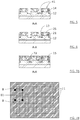
- FIG. 1 shows in top view a diagram of a substrate 1 provided, on a first face 10, with exposed zones comprising active zones 11 and electrically insulating zones 12.
- Transistor gates 21 can be formed on the basis of bars directed perpendicular to the longitudinal orientation of the active zones 11.
- CMOS components may require the addition of layers making it possible to provide stress (in compression or respectively in tension) making it possible to increase the performance of devices, in particular field effect transistors ( type P or respectively N).
- Stress layers are also called “stress liner” or CESL (Contact Etch Stop Liner).
- CESL Contact Etch Stop Liner
- Their effectiveness depends on the thickness of the layer, often made from silicon nitride. But their deposition causes filling defects which result in the short-circuiting of neighboring microelectronic components.
- the figures 2 to 7B explain these defects. They represent sectional views at the level of line AA of the figure 1 , so as to show the impact of the manufacturing steps on the electrical insulation zones. They present a summary of the successive phases of component manufacturing.
- gates 21 (generally made of polysilicon with an underlying electrically insulating layer, typically of oxide, not shown in the figures) have been manufactured. Furthermore, at this stage, spacers 22 have been formed by depositing a layer of spacers, typically silicon nitride, and etching, with well-known photolithography and etching techniques. A hard mask 23 overhangs the gate 21 of the transistors during this step which also comprises the fabrication of source / drain areas on portions of the active area where the transistor is present, these portions being adjacent to the gate of the transistor. This fabrication involves successive N-type and P-type doping to form the two types of transistors in CMOS technologies. During these steps, the electrical insulation zone 12 is affected so that a consumed zone 13 appears on its surface, in the form of hollow reliefs. This consumed zone 13 is called a cavity hereinafter.
- the step of removing the hard mask 23 presented in figure 3 worsens the consumption of the material of the electrical insulation zone 12 at the level of the cavity 13.
- the material forming the electrical insulation zone 12 is referred to hereinafter as dielectric material.
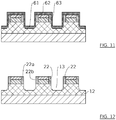
- a following step can be the deposition of a protective coating of the gates, in the form of a layer 14, for example of silicon nitride, as illustrated in figure 4 .
- this protection must then be selectively removed on the horizontal parts to clear the top of the grid and the surface of the insulation zones, with openings 41 in the protective layer 14, while preserving a protective coating on the spacers 22 This step induces additional consumption of the dielectric material.
- these steps generally include one or more heat treatments as well as cleaning phases which are also damaging to the integrity of the dielectric material.
- a mechanically constraining layer 15 can be deposited. Taking into account the undesirable consumption of the dielectric material of the zone 12 between two adjacent transistors, the aspect ratio of the cavities 13 is increased, which penalizes the reliability of the filling of the spaces between two adjacent transistors.
- the figure 7A reveals that voids 72 may remain within the mechanically constraining layer 15 itself. These residual voids 72 unfortunately cannot be filled with other layers above the mechanically constraining layer 15, such as a top layer of electrical insulator generally in silicon dioxide. This filling defect is all the more critical since the transistor stage thus formed is embedded in the middle of the line (standing for “middle of line”) of a complete microelectronic device.
- the residual voids 72 thus formed typically extend along the transverse bars 211 of the grids, from one active zone 11 to the other. This can have adverse consequences when one of these voids 72 is opened during subsequent formation of the electrical contacts, in particular when a problem with the alignment of these contacts occurs.
- the vacuum 72 thus opened is filled by the conductive material and creates a short-circuit between two contact zones of two adjacent active areas which are not intended to be electrically connected.
- the figure 7B schematically reveals two contact elements 8 present on adjacent active zones 11 and connected by a short-circuit zone 81 formed in an undesirable manner through a residual void linked to a filling defect in the mechanically constraining layer 15.
- the subject of the present invention is in particular a method for producing a component based on transistors which suppresses or limits the appearance of residual voids in the electrical insulation zones.
- One aspect relates to a method of making a component based on a plurality of transistors, on a substrate comprising at least one active area and an electrical isolation area, each transistor of the plurality of transistors comprising a gate, spacers on the sides of the gate and a contact module on an upper face of the gate, the at least one electrical insulation zone comprising at least one cavity formed as a hollow between a spacer of a first transistor of the plurality of transistors and a spacer of a second transistor of the plurality of transistors, said first transistor and second transistor being adjacent.
- This method thus provides a solution making it possible to reduce the aspect ratio of the parts of the electrical insulation zone located between two adjacent transistors, by removing side parts of the protective coating.
- the implantation phase makes it possible to make the modified portion of the protective coating very sensitive to subsequent etching, during the application of the plasma.
- the isotropic nature of the implantation ensures that the protective coating is modified as well as the horizontal parts of the device.
- the phase of applying a plasma produces a layer of silicon oxide which develops more preferably on the horizontal parts, in particular at the level of the exposed surface of the contact module and of the bottom of the cavity. These zones are therefore quickly protected, because they are covered with a layer which can be compared to a passivation layer.
- the vertical parts here essentially at the level of the protective coating, are not the place of creation of a layer of silicon oxide, or much less; therefore, these parts are attacked effectively by where the plasma species etch the material of the protective coating, typically silicon nitride.
- At least one cycle of isotropic implantation, and of application of the plasma is carried out additionally so as to eliminate as much as possible, or even completely, the protective coating, step by step.
- This reiteration ensures a progressive and precise lateral consumption of the material of the protective coating. For example, this makes it possible to eliminate it without consuming, or very little, the material of the spacers.
- Embodiments also relate to components obtained by the described aspects of the process.
- the term “on”, “overcomes”, “covers” or “underlying” or their equivalents do not necessarily mean “in contact with”.
- the deposition of a first layer on a second layer does not necessarily mean that the two layers are directly in contact with each other, but it does mean that the first layer at least partially covers the second layer. by being either directly in contact with it or by being separated from it by at least one other layer or at least one other element.
- a layer can also be made up of several sub-layers of the same material or of different materials.
- a substrate By a substrate, a layer, a device, “based” on a material M, is meant a substrate, a layer, a device comprising this material M only or this material M and possibly other materials, for example elements. alloy, impurities or doping elements.
- a spacer based on silicon nitride SiN can for example comprise non-stoichiometric silicon nitride (SiN), or stoichiometric silicon nitride (Si3N4), or else an oxy-nitride of silicon (SiON).
- the layer based on a silicon oxide formed by the plasma may comprise at least 50% of this oxide, or even be only a layer consisting of this oxide.
- device or microelectronic device element is meant any type of element produced with the means of microelectronics.
- These devices include in particular, in addition to purely electronic devices, micromechanical or electromechanical devices (MEMS, NEMS, etc.) as well as optical or optoelectronic devices (MOEMS, etc.).
- MEMS micromechanical or electromechanical devices
- MOEMS optical or optoelectronic devices
- successive steps of the manufacturing process are described below.
- the adjective “successive” does not necessarily imply, even if this is generally preferred, that the steps follow each other immediately, intermediate steps being able to separate them.
- the term “step” is understood to mean carrying out part of the process, and can designate a set of sub-steps.
- dielectric qualifies a material whose electrical conductivity is sufficiently low in the given application to serve as an insulator.
- a dielectric material preferably has a dielectric constant of less than 7.
- STIs and spacers are typically formed from a dielectric material.
- a cavity 13 corresponds to a void formed within the electrical insulation zone 12, this void being open at the surface of said electrical insulation zone 12, this void further extending between two spacers 22 of two adjacent respective transistors, in line with said spacers 22.
- the hollow formed by the cavity 13 is understood with respect to a plane coincident with the isolation zone / gate interface.
- thickness for a layer height for a device (transistor or gate for example) and depth for a cavity or an etching.
- the thickness is taken in a direction normal to the main extension plane of the layer, the height and depth are taken in a direction normal to the base plane of the substrate.
- the orientation of the thickness may vary; on the sides of the grid, for example, the thickness of the spacers or of the protective coating is generally parallel to the plane of the substrate.
- a spacer forms a ring around the grid, with a closed contour; we could therefore speak of a single spacer around the grid; however, the cross-sectional representations, and the preferred directions of the grids, mean that we also speak of pairs of spacers (or first and second spacers), terminology used here.
- a direction substantially normal to a plane means a direction having an angle of 90 ⁇ 10 ° with respect to the plane.
- the chemical compositions of the different layers or regions can be determined using the well-known EDX or X-EDS method, acronym for “energy dispersive x-ray spectroscopy” which means “energy dispersive analysis of X photons”.
- This method is well suited for analyzing the composition of portions of small dimensions such as cavities filled with the filling material. It can be implemented on metallurgical sections within a SEM or a TEM.
- the size of the residual voids and / or the cavities filled with a filling material are characteristic of the implementation of the method. They can therefore be an index of the implementation of the method according to the invention.
- the method comprises a part of conventional manufacturing steps of transistors aiming to form on a substrate, for each of the transistors, a pattern or a gate area 100 flanked by spacers 22.
- the steps of figures 1 to 6 can in particular be performed. It can be referred to for the steps described immediately below.
- the substrate 1 can comprise a so-called massive or “bulk” part according to English terminology, active zones 11 made of semiconductor material, and insulation zones 12 made of dielectric material.
- the substrate may also be of the semiconductor-on-insulator type, for example a silicon-on-insulator SOI (acronym for “silicon on insulator) substrate or a germanium-on-insulator GeOI (acronym for“ germanium on insulator) substrate.
- SOI silicon-on-insulator
- GeOI germanium-on-insulator
- the transistors are formed on active areas 11 and electrically isolated by isolation areas 12, typically STI (shallow trench isolation) type isolation trenches, generally based on silicon oxide.
- isolation areas 12 typically STI (shallow trench isolation) type isolation trenches, generally based on silicon oxide.
- the gate pattern 100 typically comprises a gate 21 and a hard mask 23 made of nitride, and typically silicon nitride (SiN). It can have a width known as the critical dimension of between 10 nm and 100 nm and preferably less than or equal to 50 nm.
- the grid pattern can have a height of the order of a few tens of nanometers.
- the grid 21 typically has a height less than or equal to 100 nm, for example approximately equal to 50 nm.
- the height of the hard mask 23 is generally between 40 and 80 nanometers.
- Two neighboring gate patterns are separated by a pitch “p” typically less than or equal to 120 nm.
- the same grid pattern 100 can alternately overcome one or more active areas 11 and one or more adjacent STI trenches 12.
- Spacers 22 are formed along the flanks of this grid pattern 1.
- the flanks of the grid patterns extend in planes substantially normal to the base plane of the substrate.
- the formation of these spacers 22 generally comprises a conformal deposition of a layer of SiN on and between the gate patterns 1, followed by an anisotropic etching of the SiN, in a direction substantially parallel to the flanks of the gate patterns. .
- the deposition can typically be done by PEALD, so as to form a layer of SiN having a thickness less than or equal to 15 nm, for example between 6 nm and 15 nm, preferably between 8 nm and 12 nm.
- a dielectric material of the Low-k type (of dielectric constant k ⁇ 7) can be used to form the spacers 22.
- this material can be SiBCN or SiCO.
- the “SiN layer” to which reference is made for the sake of clarity can therefore be understood as “the layer of a low-k type dielectric material used to form the spacers 22”.
- the anisotropic etching is configured to consume the portions of SiN layer located at the top of the gate patterns 100 and between the gate patterns 100, on part of the zones 12. It can be carried out by plasma, for example based on a fluorocarbon-type chemistry, in an inductively coupled plasma reactor (ICP) (Inductively Coupled Plasma).
- ICP inductively coupled plasma reactor
- the form factor of the grid patterns 100 generally induces a faster consumption of the layer portions at the base of the grid patterns, on the substrate, compared to the layer portions at the top of the grid patterns.
- cavities 13 form on the surface of the exposed STI trenches 12.
- these cavities 13 can develop and their depth can increase.
- the following steps may include high temperature anneals.
- a diffusion annealing and / or activation of the dopants implanted during the second ion implantation can be carried out.
- a protective layer preferably of SiN is deposited and then etched anisotropically to obtain the result of the figure 5 . Lateral portions of the protective layer are thus preserved on the sides of the first spacers 22 to form a protective coating 24. The latter preferably extends over the entire exposed surface of the spacers 22.
- a step of siliciding a portion 25 of the gate zone can also be carried out.
- This step comprises the deposition of a metal, for example nickel (Ni), on the top of the grids 21, and several thermal anneals aimed in particular at diffusing the metal in the grid (diffusion annealing) to form a silicide (NiSi or NiPtSi) and to passivate electrically active faults (DSA type activation annealing, acronym for “Dynamic Surface Anneal”).
- a metal for example nickel (Ni)
- thermal anneals aimed in particular at diffusing the metal in the grid
- DSA type activation annealing acronym for “Dynamic Surface Anneal”.
- DSA type activation annealing acronym for “Dynamic Surface Anneal”.
- the figure 8 reflects a configuration of the component at this point, in which the protective covering 24 occupies a significant lateral space, extending laterally from the spacers 22 and covering the wall of the cavities 13 which were formed during the previous stages.
- the interstitial space between two adjacent transistors is found to be reduced by this protective layer, and the aspect ratio of this zone, in particular at the bottom of cavity 13, is increased, which is detrimental for subsequent layer deposition steps.
- the present invention seeks to reduce the lateral extension of the protective covering 24, or even to eliminate it.
- the method of the invention comprises an implantation step making it possible to form modified surface parts of the exposed surfaces.
- the figure 9 presents such a modification, in particular with a modified part 51 of the base portion (formed by an exposed surface of the material of the electrical insulation zone 12), of the cavity 13, a modified part 52 of the contact module 25 and a modified portion 53 of the protective coating 24.
- the wafer 221 exposed on the upper face of the spacers 22 may also be modified thereby.
- this implantation is carried out with light ions, that is to say having low atomic numbers, preferably equal to one or two.
- the preferred species are based on hydrogen and helium. It may be dihydrogen and / or helium or a mixture of the two, or else other compounds comprising hydrogen and / or helium, such as HBr or NH 3 .
- this phase of implantation is isotropic so as to produce a modification on an equivalent or equal thickness whether it is on the horizontal parts or on the vertical parts.
- a plasma etching reactor of different types and in particular of the "ICP” type (standing for inductively coupled plasma, that is to say inductively coupled plasma), or of the "CCP” type. ”(Capacitively coupled plasma, ie capacitively coupled plasma). It is also possible to use plasmas by immersion.
- the operation time is advantageously short enough so as to modify a small thickness.
- This time can be configured so that the modified thickness is less than or equal to 5 nm, preferably less than or equal to 3 nm.
- the time of this operation may be less than or equal to 30 seconds and / or greater than or equal to 5 seconds, and preferably less than or equal to 10 seconds and / or greater than or equal to 5 seconds.
- the power of the source can be between 100 and 2000 W, is for example 500 W and / or the polarization power can be between 20 and 2000 W, and for example 250 W.
- the polarization power can be between 20 and 2000 W, and for example 250 W.
- a plasma is then applied comprising a mixture of gaseous components.
- this mixture comprises a first component which includes at least one chlorinated species and / or at least one fluorinated species. It is possible to use SiCl 4 , or even SiF 4 in particular.
- the first component has the advantage of etching the modified surface part 53 of the protective coating 24.
- one aspect of the invention is the formation of a protective layer on the exposed surfaces for which etching is not desired, in particular at the horizontal parts corresponding to the exposed surface of the contact module. 25 and to the base portion 41 of the cavities 13.
- one aspect of the invention is to play on the propensity for the formation of a layer of a silicon oxide on materials used for the contact module 25. and for the electrical insulation zone, while this formation is much slower, or even almost non-existent, on the material of the protective coating 24, even modified (in this context, the figure 10 does not show an oxide layer at the level of the protective coating 24).
- the application of the plasma is configured so that the formation of the oxide layer on the protective coating is at most 2 nm.
- a layer of a silicon oxide of general form SiO x
- SiO x the combined action of the etching of the modified parts of the protective coating 53 and the formation of a layer of silicon oxide appears on the figure 10 . It is then noted that a residual part 54 of the protective coating 24 is preserved and that a layer of silicon oxide 61, 62 is present at the initial location of the protective coating 24. It is understood that the silicon oxide layer ensures passivation of the surfaces in question so as to make them insensitive to etching targeting the protective coating 24.
- the gas mixture comprises at least one component including the oxygen species. This is typically oxygen O 2, which is also used to adjust the dilution of the other components of the mixture.
- the gas mixture advantageously comprises a fluorocarbon gas, and more preferably a hydrofluorocarbon gas, of general formula C x H y F z .
- this gas enhances the etching action of the modified part of the protective coating 24. It can also serve to attack the residual part of this protective coating, when the modified part has been completely removed.
- a reactor corresponding to one of the types indicated above can be used for the implantation phase.
- the implantation step and the plasma application step take place in the same reactor. This is also preferably the case with the additional implantation and application steps then carried out and described below.
- the lateral extension of the protective covering 24 has been significantly reduced, since only a residual part 54 remains. If the initial layer 24 is sufficiently thin with regard to the etching conditions, it can be completely removed at this stage.
- the repetition of these steps makes it possible to gradually eliminate the protective coating 24 while avoiding too thick deposition of the silicon oxide on this protective coating, which could occur if a single plasma application step were implemented.
- the additional implantation is advantageously configured to attack the layer of silicon oxide; this etching makes it possible to reduce the thickness on the horizontal parts and, preferentially, to completely remove the silicon oxide layer on the vertical parts, that is to say at the level of the protective coating 24.
- the implantation and plasma application times can be adjusted to limit the thicknesses treated.
- the figure 11 shows the result of an additional implantation making it possible to form new modified parts including a new modified part at the level of the protective coating and an additional application of a plasma.
- the figure 12 shows the result after at least one additional implantation and at least one additional application of plasma, and after a final cleaning step.
- This step is configured to remove the layer of silicon oxide which may remain, in particular at the level of the surfaces of the base portion of the cavity 13 and of the upper face of the contact module 25, as was the case above. figure 11 , under references 61 and 62.
- one embodiment consists in using wet etching, for example based on hydrofluoric acid.
- the etching solution is strongly diluted so as to remove the silicon oxide which had been deposited, without attacking, or as little as possible, the underlying layers, and in particular the material of the electrical insulation zone 12.
- the result reflected in the figure 12 is a succession of transistors between which the distances between the spacers 22 of different transistors have been increased, without however hollowing out the cavities 13, so that the aspect ratio obtained at this location is reduced and is much more favorable to the following steps, and in particular at the step of forming a mechanically constraining layer.
- the formation of voids is greatly reduced or even completely eliminated.
- the deposition of the stress liner (that is to say the mechanically constraining layer) can then be carried out (not illustrated) while limiting the appearance of residual voids.
- the stress liner is a layer of nitride, in particular a layer of silicon nitride (SiN or SixNy x and y being integers).
- PECVD plasma-assisted chemical vapor deposition
- LPCVD low pressure chemical vapor deposition
- RTCVD rapid CVD thermal deposition
- PVD physical vapor deposition
- ALD atomic layer deposition
- the stress liner can have a thickness of a few nanometers to a few tens of nanometers, and in particular a thickness of between 5 and 40 nanometers, for example 20 nm.
- stress liner it is not excluded to deposit a plurality of stress liner or to limit the deposition of the stress liner to one area of the face of the substrate, and, optionally, to coat at least one other area of the face of the substrate with at least one another stress liner, for example to implement mechanical stresses of opposite signs (in compression and in tension).
- One advantage of the invention is to increase the manufacturing reliability of transistors.
- the subsequent steps of forming the electrical contacts on the electrically active zones of the transistors can in particular be carried out without risk of a short-circuit between two active zones 11 linked to an untimely filling of a residual vacuum at the level. of TSIs 12.
Landscapes
- Insulated Gate Type Field-Effect Transistor (AREA)
- Chemical & Material Sciences (AREA)
- Chemical Kinetics & Catalysis (AREA)
- General Chemical & Material Sciences (AREA)
- Metal-Oxide And Bipolar Metal-Oxide Semiconductor Integrated Circuits (AREA)
- Internal Circuitry In Semiconductor Integrated Circuit Devices (AREA)
Applications Claiming Priority (1)
| Application Number | Priority Date | Filing Date | Title |
|---|---|---|---|
| FR1909377A FR3100085B1 (fr) | 2019-08-23 | 2019-08-23 | procédé de fabrication de composants micro-électroniques |
Publications (1)
| Publication Number | Publication Date |
|---|---|
| EP3783643A1 true EP3783643A1 (de) | 2021-02-24 |
Family
ID=68281704
Family Applications (1)
| Application Number | Title | Priority Date | Filing Date |
|---|---|---|---|
| EP20188404.6A Pending EP3783643A1 (de) | 2019-08-23 | 2020-07-29 | Verfahren zur herstellung von mikroelektronischen komponenten |
Country Status (3)
| Country | Link |
|---|---|
| US (1) | US11244868B2 (de) |
| EP (1) | EP3783643A1 (de) |
| FR (1) | FR3100085B1 (de) |
Families Citing this family (1)
| Publication number | Priority date | Publication date | Assignee | Title |
|---|---|---|---|---|
| US11967636B2 (en) | 2021-10-19 | 2024-04-23 | Global Foundries U.S. Inc. | Lateral bipolar junction transistors with an airgap spacer |
Citations (5)
| Publication number | Priority date | Publication date | Assignee | Title |
|---|---|---|---|---|
| US20030136332A1 (en) * | 2002-01-24 | 2003-07-24 | Applied Materials Inc., A Delaware Corporation | In situ application of etch back for improved deposition into high-aspect-ratio features |
| US20120025318A1 (en) * | 2010-07-30 | 2012-02-02 | Globalfoundries Inc. | Reduced Topography in Isolation Regions of a Semiconductor Device by Applying a Deposition/Etch Sequence Prior to Forming the Interlayer Dielectric |
| US20120025323A1 (en) * | 2010-07-29 | 2012-02-02 | Taiwan Semiconductor Manufacturing Company, Ltd. | Spacer structures of a semiconductor device |
| US20140179107A1 (en) * | 2012-12-21 | 2014-06-26 | Intermolecular Inc. | Etching Silicon Nitride Using Dilute Hydrofluoric Acid |
| EP3246953A1 (de) * | 2016-05-20 | 2017-11-22 | Commissariat à l'Energie Atomique et aux Energies Alternatives | Verfahren zur herstellung von transistoren, die unterschiedliche eigenschaften aufweisen, auf demselben substrat |
Family Cites Families (2)
| Publication number | Priority date | Publication date | Assignee | Title |
|---|---|---|---|---|
| KR20120010642A (ko) * | 2010-07-22 | 2012-02-06 | 삼성전자주식회사 | 비휘발성 메모리 소자, 그 제조 방법 및 그 구동 방법 |
| US10700173B2 (en) * | 2018-04-10 | 2020-06-30 | Globalfoundries Inc. | FinFET device with a wrap-around silicide source/drain contact structure |
-
2019
- 2019-08-23 FR FR1909377A patent/FR3100085B1/fr active Active
-
2020
- 2020-07-29 EP EP20188404.6A patent/EP3783643A1/de active Pending
- 2020-08-21 US US16/999,642 patent/US11244868B2/en active Active
Patent Citations (5)
| Publication number | Priority date | Publication date | Assignee | Title |
|---|---|---|---|---|
| US20030136332A1 (en) * | 2002-01-24 | 2003-07-24 | Applied Materials Inc., A Delaware Corporation | In situ application of etch back for improved deposition into high-aspect-ratio features |
| US20120025323A1 (en) * | 2010-07-29 | 2012-02-02 | Taiwan Semiconductor Manufacturing Company, Ltd. | Spacer structures of a semiconductor device |
| US20120025318A1 (en) * | 2010-07-30 | 2012-02-02 | Globalfoundries Inc. | Reduced Topography in Isolation Regions of a Semiconductor Device by Applying a Deposition/Etch Sequence Prior to Forming the Interlayer Dielectric |
| US20140179107A1 (en) * | 2012-12-21 | 2014-06-26 | Intermolecular Inc. | Etching Silicon Nitride Using Dilute Hydrofluoric Acid |
| EP3246953A1 (de) * | 2016-05-20 | 2017-11-22 | Commissariat à l'Energie Atomique et aux Energies Alternatives | Verfahren zur herstellung von transistoren, die unterschiedliche eigenschaften aufweisen, auf demselben substrat |
Also Published As
| Publication number | Publication date |
|---|---|
| US20210057283A1 (en) | 2021-02-25 |
| US11244868B2 (en) | 2022-02-08 |
| FR3100085A1 (fr) | 2021-02-26 |
| FR3100085B1 (fr) | 2022-08-12 |
Similar Documents
| Publication | Publication Date | Title |
|---|---|---|
| EP2999001B1 (de) | Einbringung von abstandhaltern an den seiten eines transistor-gates | |
| EP2876677A1 (de) | Verfahren zur Bildung von Abstandhaltern eines Gates eines Transistors | |
| FR3046290B1 (fr) | Methode de realisation d'espaceurs a faible permittivite | |
| EP2610915A1 (de) | Transistor und Herstellungsverfahren eines Transistors | |
| EP3783644B1 (de) | Verfahren zur herstellung von mikroelektronischen komponenten | |
| EP3246948B1 (de) | Verfahren zur herstellung von transistoren, die unterschiedliche eigenschaften aufweisen, auf demselben substrat | |
| FR3047352A1 (fr) | Procede de fabrication d'un transistor a dopant localise a l'aplomb de la grille | |
| EP3783643A1 (de) | Verfahren zur herstellung von mikroelektronischen komponenten | |
| EP4006996B1 (de) | Quantenvorrichtung und ihr herstellungsverfahren | |
| FR3037714A1 (fr) | Procede de realisation d'un contact sur une zone active d'un circuit integre, par exemple realise sur un substrat du type soi, en particulier fdsoi, et circuit integre correspondant | |
| EP3961689A1 (de) | Verfahren zur herstellung von mikroelektronischen komponenten | |
| FR2976401A1 (fr) | Composant electronique comportant un ensemble de transistors mosfet et procede de fabrication | |
| EP4050642A1 (de) | Verfahren zur bildung von abstandhaltern eines gates eines transistors | |
| EP4002482B1 (de) | Verfahren zur herstellung eines bereichs, der mit einer mikroelektronischen vorrichtung dotiert ist | |
| FR2947384A1 (fr) | Procede de realisation d'un transistor a source et drain metalliques | |
| FR3098981A1 (fr) | procédé de fabrication de transistors | |
| EP3667734B1 (de) | Herstellungsverfahren von mikroelektronischen komponenten | |
| EP3503203A1 (de) | Herstellung von transistoren mit unter spannung stehenden kanälen | |
| EP3764390A1 (de) | Verfahren zur bildung von abstandhaltern für einen transistor | |
| EP4053883B1 (de) | Verfahren zum ätzen einer dielektrischen dreidimensionalen schicht | |
| FR3023408A1 (fr) | Procede de fabrication d'une cellule memoire a double grille | |
| FR3098978A1 (fr) | procédé de fabrication de transistors | |
| EP4391082A1 (de) | Verfahren zur herstellung einer halbleiteranordnung mit einem rückgitter | |
| WO2025056260A1 (fr) | Procédé de réalisation de transistors mosfet intégrant des cavités d'air pour la réduction du couplage capacitif en régime radiofréquence | |
| EP4053884A1 (de) | Verfahren zum ätzen einer dielektrischen dreidimensionalen schicht |
Legal Events
| Date | Code | Title | Description |
|---|---|---|---|
| PUAI | Public reference made under article 153(3) epc to a published international application that has entered the european phase |
Free format text: ORIGINAL CODE: 0009012 |
|
| STAA | Information on the status of an ep patent application or granted ep patent |
Free format text: STATUS: REQUEST FOR EXAMINATION WAS MADE |
|
| 17P | Request for examination filed |
Effective date: 20200729 |
|
| AK | Designated contracting states |
Kind code of ref document: A1 Designated state(s): AL AT BE BG CH CY CZ DE DK EE ES FI FR GB GR HR HU IE IS IT LI LT LU LV MC MK MT NL NO PL PT RO RS SE SI SK SM TR |
|
| AX | Request for extension of the european patent |
Extension state: BA ME |
|
| STAA | Information on the status of an ep patent application or granted ep patent |
Free format text: STATUS: EXAMINATION IS IN PROGRESS |
|
| 17Q | First examination report despatched |
Effective date: 20220803 |
|
| RAP3 | Party data changed (applicant data changed or rights of an application transferred) |
Owner name: COMMISSARIAT A L'ENERGIE ATOMIQUE ET AUX ENERGIESALTERNATIVES |