EP3809455A1 - Verfahren zur herstellung eines integrierten schaltkreises, der eine phase zur bildung von gräben in einem substrat umfasst, und entsprechender integrierter schaltkreis - Google Patents
Verfahren zur herstellung eines integrierten schaltkreises, der eine phase zur bildung von gräben in einem substrat umfasst, und entsprechender integrierter schaltkreis Download PDFInfo
- Publication number
- EP3809455A1 EP3809455A1 EP20200176.4A EP20200176A EP3809455A1 EP 3809455 A1 EP3809455 A1 EP 3809455A1 EP 20200176 A EP20200176 A EP 20200176A EP 3809455 A1 EP3809455 A1 EP 3809455A1
- Authority
- EP
- European Patent Office
- Prior art keywords
- zone
- barrier layer
- substrate
- trench
- depth
- Prior art date
- Legal status (The legal status is an assumption and is not a legal conclusion. Google has not performed a legal analysis and makes no representation as to the accuracy of the status listed.)
- Pending
Links
Images


Classifications
-
- H—ELECTRICITY
- H10—SEMICONDUCTOR DEVICES; ELECTRIC SOLID-STATE DEVICES NOT OTHERWISE PROVIDED FOR
- H10W—GENERIC PACKAGES, INTERCONNECTIONS, CONNECTORS OR OTHER CONSTRUCTIONAL DETAILS OF DEVICES COVERED BY CLASS H10
- H10W10/00—Isolation regions in semiconductor bodies between components of integrated devices
- H10W10/01—Manufacture or treatment
- H10W10/011—Manufacture or treatment of isolation regions comprising dielectric materials
- H10W10/014—Manufacture or treatment of isolation regions comprising dielectric materials using trench refilling with dielectric materials, e.g. shallow trench isolations
- H10W10/0143—Manufacture or treatment of isolation regions comprising dielectric materials using trench refilling with dielectric materials, e.g. shallow trench isolations comprising concurrently refilling multiple trenches having different shapes or dimensions
-
- H—ELECTRICITY
- H10—SEMICONDUCTOR DEVICES; ELECTRIC SOLID-STATE DEVICES NOT OTHERWISE PROVIDED FOR
- H10W—GENERIC PACKAGES, INTERCONNECTIONS, CONNECTORS OR OTHER CONSTRUCTIONAL DETAILS OF DEVICES COVERED BY CLASS H10
- H10W10/00—Isolation regions in semiconductor bodies between components of integrated devices
- H10W10/01—Manufacture or treatment
- H10W10/011—Manufacture or treatment of isolation regions comprising dielectric materials
- H10W10/014—Manufacture or treatment of isolation regions comprising dielectric materials using trench refilling with dielectric materials, e.g. shallow trench isolations
-
- H—ELECTRICITY
- H10—SEMICONDUCTOR DEVICES; ELECTRIC SOLID-STATE DEVICES NOT OTHERWISE PROVIDED FOR
- H10B—ELECTRONIC MEMORY DEVICES
- H10B41/00—Electrically erasable-and-programmable ROM [EEPROM] devices comprising floating gates
- H10B41/40—Electrically erasable-and-programmable ROM [EEPROM] devices comprising floating gates characterised by the peripheral circuit region
- H10B41/42—Simultaneous manufacture of periphery and memory cells
- H10B41/43—Simultaneous manufacture of periphery and memory cells comprising only one type of peripheral transistor
- H10B41/47—Simultaneous manufacture of periphery and memory cells comprising only one type of peripheral transistor with a floating-gate layer also being used as part of the peripheral transistor
-
- H—ELECTRICITY
- H10—SEMICONDUCTOR DEVICES; ELECTRIC SOLID-STATE DEVICES NOT OTHERWISE PROVIDED FOR
- H10P—GENERIC PROCESSES OR APPARATUS FOR THE MANUFACTURE OR TREATMENT OF DEVICES COVERED BY CLASS H10
- H10P14/00—Formation of materials, e.g. in the shape of layers or pillars
- H10P14/60—Formation of materials, e.g. in the shape of layers or pillars of insulating materials
- H10P14/69—Inorganic materials
- H10P14/694—Inorganic materials composed of nitrides
- H10P14/6943—Inorganic materials composed of nitrides containing silicon
- H10P14/69433—Inorganic materials composed of nitrides containing silicon the material being a silicon nitride not containing oxygen, e.g. SixNy or SixByNz
-
- H—ELECTRICITY
- H10—SEMICONDUCTOR DEVICES; ELECTRIC SOLID-STATE DEVICES NOT OTHERWISE PROVIDED FOR
- H10P—GENERIC PROCESSES OR APPARATUS FOR THE MANUFACTURE OR TREATMENT OF DEVICES COVERED BY CLASS H10
- H10P50/00—Etching of wafers, substrates or parts of devices
- H10P50/20—Dry etching; Plasma etching; Reactive-ion etching
- H10P50/28—Dry etching; Plasma etching; Reactive-ion etching of insulating materials
- H10P50/282—Dry etching; Plasma etching; Reactive-ion etching of insulating materials of inorganic materials
- H10P50/283—Dry etching; Plasma etching; Reactive-ion etching of insulating materials of inorganic materials by chemical means
-
- H—ELECTRICITY
- H10—SEMICONDUCTOR DEVICES; ELECTRIC SOLID-STATE DEVICES NOT OTHERWISE PROVIDED FOR
- H10P—GENERIC PROCESSES OR APPARATUS FOR THE MANUFACTURE OR TREATMENT OF DEVICES COVERED BY CLASS H10
- H10P50/00—Etching of wafers, substrates or parts of devices
- H10P50/69—Etching of wafers, substrates or parts of devices using masks for semiconductor materials
- H10P50/691—Etching of wafers, substrates or parts of devices using masks for semiconductor materials for Group V materials or Group III-V materials
-
- H—ELECTRICITY
- H10—SEMICONDUCTOR DEVICES; ELECTRIC SOLID-STATE DEVICES NOT OTHERWISE PROVIDED FOR
- H10P—GENERIC PROCESSES OR APPARATUS FOR THE MANUFACTURE OR TREATMENT OF DEVICES COVERED BY CLASS H10
- H10P52/00—Grinding, lapping or polishing of wafers, substrates or parts of devices
- H10P52/40—Chemomechanical polishing [CMP]
- H10P52/402—Chemomechanical polishing [CMP] of semiconductor materials
-
- H—ELECTRICITY
- H10—SEMICONDUCTOR DEVICES; ELECTRIC SOLID-STATE DEVICES NOT OTHERWISE PROVIDED FOR
- H10W—GENERIC PACKAGES, INTERCONNECTIONS, CONNECTORS OR OTHER CONSTRUCTIONAL DETAILS OF DEVICES COVERED BY CLASS H10
- H10W10/00—Isolation regions in semiconductor bodies between components of integrated devices
- H10W10/10—Isolation regions comprising dielectric materials
- H10W10/17—Isolation regions comprising dielectric materials formed using trench refilling with dielectric materials, e.g. shallow trench isolations
-
- H—ELECTRICITY
- H10—SEMICONDUCTOR DEVICES; ELECTRIC SOLID-STATE DEVICES NOT OTHERWISE PROVIDED FOR
- H10W—GENERIC PACKAGES, INTERCONNECTIONS, CONNECTORS OR OTHER CONSTRUCTIONAL DETAILS OF DEVICES COVERED BY CLASS H10
- H10W90/00—Package configurations
-
- H—ELECTRICITY
- H10—SEMICONDUCTOR DEVICES; ELECTRIC SOLID-STATE DEVICES NOT OTHERWISE PROVIDED FOR
- H10W—GENERIC PACKAGES, INTERCONNECTIONS, CONNECTORS OR OTHER CONSTRUCTIONAL DETAILS OF DEVICES COVERED BY CLASS H10
- H10W10/00—Isolation regions in semiconductor bodies between components of integrated devices
- H10W10/01—Manufacture or treatment
- H10W10/011—Manufacture or treatment of isolation regions comprising dielectric materials
- H10W10/014—Manufacture or treatment of isolation regions comprising dielectric materials using trench refilling with dielectric materials, e.g. shallow trench isolations
- H10W10/0145—Manufacture or treatment of isolation regions comprising dielectric materials using trench refilling with dielectric materials, e.g. shallow trench isolations of trenches having shapes other than rectangular or V-shape
Definitions
- Embodiments and embodiments relate to integrated circuits, in particular the formation of trenches in a semiconductor substrate.
- trenches in the semiconductor substrate of an integrated circuit is used in many respects.
- a trench formation phase is typically provided for the fabrication of lateral insulation regions (usually designated by the acronym "STI” from the English term “Shallow Trench Isolation”).
- STI shallow Trench Isolation
- the lateral isolation trenches make it possible to electrically isolate, for example, transistors, which can be incorporated in a logic part or in a region of non-volatile memory.
- the side isolation trenches located in the logic part and in the non-volatile memory part are made simultaneously and have the same structure.
- the logic part typically comprises implantations of dopants in large quantities, which generate crystalline defects which can cause dislocations, if the mechanical stresses are high.
- the volume of dielectric of the side insulation trenches can cause such stresses, and it would be desirable in this regard to decrease the volume of dielectric.
- a phase of forming trenches in the semiconductor substrate of an integrated circuit can also be provided for the manufacture of the vertical gates of buried transistors with vertical gates, or for the manufacture of vertical capacitive elements in the substrate.
- the trenches intended to receive vertical grids or electrodes of capacitive elements are formed simultaneously, or even simultaneously also with the formation of the lateral insulation trenches.
- the depth of the trenches accommodating the vertical gates influences the performance of the buried transistors and the other steps in the fabrication of the buried transistors, an established depth is therefore very difficult to modify.
- Dissociating the fabrications of trenches in the semiconductor substrate in the different parts of the substrate, depending on the use of the trench, is not envisaged in industrial productions for reasons of cost (except possibly exceptionally for very specific needs) .
- a single dry etching step makes it possible to form trenches of different depths in the first zone and in the second zone.
- the difference between the depths is obtained by the time devoted to the etching of the second stop layer in the second zone which is not devoted to the etching of the trench in the substrate in the total duration of the given time of the etching. dried.
- the formation of the second barrier layer is not critical with respect to alignment or the materials used, and the cost of its use is moderate.
- the method further comprises removing the entire second barrier layer.
- the method further comprises, after the dry etching, a wet etching configured to laterally remove a portion of the first barrier layer on the sides etched by the dry etching, in which the second layer of The stopper is configured so that said wet etching produces said removal of the entire second stopper layer.
- a wet etching already provided in an etching process to remove a side portion of the first barrier layer, usually called “nitride pull back”, in order to completely remove the second layer. stop.
- the second layer is advantageously configured to react appropriately to the wet etching as initially intended, i.e. to be completely removed.
- the first barrier layer and the second barrier layer comprise silicon nitride
- the second barrier layer comprises dopants at a concentration chosen so that said wet etching produces said removal of the second stop coat in full.
- the first stopper layer comprises silicon nitride
- the second stopper layer comprises a material, different from the silicon nitride of the first stopper layer, configured so that said etching wet produces said shrinkage of the entire second barrier layer.
- the second barrier layer is advantageously chosen with respect to dry etching in order to introduce a certain depth differential of the trenches of the first zone and of the second zone, and also with respect to wet etching to be completely removed during the step of removing a lateral portion on the sides of the first stop layer (“nitride pull back” step).
- doping with silicon nitride makes it possible to configure the reactivity of the second barrier layer with the wet etching, and thus to configure the thickness of this layer and therefore also the difference between the depths.
- the method comprises an excess filling of the trenches with a dielectric material, and a chemical-mechanical polishing stopped by the first stop layer, the trenches thus filled being intended to form trenches of side insulation.
- the method may advantageously include removing the entire second barrier layer to simplify detection of the first barrier layer to stop chemical mechanical polishing.
- This latter mode of implementation is well suited, but not essential, when the method further comprises steps of forming a non-volatile memory in the first zone of the substrate, and steps of forming a logic part in the second area of the substrate.
- the method comprises forming a dielectric envelope on the sides and the bottom of the trenches, excess filling of the trenches with a conductive material, and mechanical-chemical polishing stopped by the first stop layer, the trenches thus filled in the first zone being intended to form vertical electrodes of capacitive elements, the trenches thus filled in the second zone being intended to form vertical gates of buried transistors.
- the method may advantageously comprise removing the entire second barrier layer in order to simplify the detection of the first barrier layer from chemical mechanical polishing.
- This latter mode of implementation is well suited, but not essential, when the method further comprises steps of forming a capacitive element in the first zone of the substrate, and steps of forming a non-volatile memory in the second area of the substrate.
- the difference between the first depth and the second depth is between 10nm and 100nm.
- an integrated circuit comprising a semiconductor substrate having a front face, a first region of the substrate comprising at least a first element formed in a first trench extending vertically in the substrate at a first depth with respect to at the front face, and a second zone of the substrate comprising at least a second element formed in a second trench extending vertically in the substrate at a second depth relative to the front face, the second depth being less than the first depth.
- the method comprises a transition trench delimiting the first zone on one side of the transition trench and the second zone on the other side of the transition trench, the bottom of the transition trench being asymmetric. relative to a median plane of the transition trench and located between said side and said other side.
- the bottom of the transition trench comprises a lower part, on the side of the first zone, and an upper part, shallower than the lower part, on the side of the second zone.
- An inclined plane connects the lower part and the upper part in the bottom of the transition trench.
- said at least one first element comprises a lateral insulation trench and said at least one second element comprises a lateral insulation trench.
- This latter embodiment is well suited, but not essential, when the first zone comprises a non-volatile memory, and the second zone comprises a logic part.
- non-volatile memory thus benefits from better lateral insulation reducing the parasitic effects of leaks, and the logic part benefits from less mechanical stresses reducing the risks of dislocation.
- said at least one first element comprises a vertical gate of a buried transistor
- said at least one at least a second element comprises a vertical electrode of a capacitive element
- This latter embodiment is well suited, but not essential, when the first zone comprises a capacitive element, and the second zone comprises a non-volatile memory.
- the vertical electrode can thus cover a greater surface area deep in the substrate, and the surface capacitive value of the capacitive element can thus be increased, without being limited by an established depth of the trenches of the buried transistors.
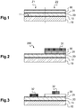
- the figure 1 illustrates the result of a step of a phase of forming trenches in a semiconductor substrate 10, in an integrated circuit manufacturing process.
- the semiconductor substrate 10 is for example formed from silicon and comprises a first zone Z1 and a second zone Z2.
- the first zone Z1 may be intended to include a non-volatile memory region and the second zone Z2 may be intended to include a logic part, for example both incorporated in a microcontroller.
- the first zone Z1 can be intended to include a capacitive element with a vertical structure in the substrate, and the second zone Z2 can be intended to include a non-volatile memory, for example both incorporated in a microcontroller.
- the capacitive element may have a vertical structure such as, for example, described in French patent applications no. 1757907 , n ° 1757906 , or n ° 1902278 .
- the substrate 10 comprises a front face 11, which corresponds to the face of the substrate 10 from which will be produced electronic components, such as transistors or diodes, in the part otherwise designated “FEOL” for “Front End Of Line”. »According to the usual English term.
- the front face 11 has been covered with a conventional buffer oxide layer 15.
- the buffer oxide layer comprises approximately 7 nm of silicon dioxide obtained by deposition or growth.
- a first barrier layer 20 has been formed on the buffer oxide layer 15 on the front face 11 of the substrate 10, in the first zone Z1 and in the second zone Z2.
- the first barrier layer 20 is formed of silicon nitride, and is obtained by low pressure chemical vapor deposition ("LPCVD").
- the first barrier layer 20 can have a thickness of about 80 nm.
- a second barrier layer 30 has been formed on the first barrier layer 20, in the first zone Z1 and in the second zone Z2.
- the first barrier layer 30 is formed from doped silicon nitride, and is obtained by chemical vapor deposition in a plasma environment (“PECVD”). The doping can be carried out in-situ during the deposition or ex-situ by a subsequent implantation.
- the second barrier layer 30 can have a thickness of about 40 nm. Reference will be made to the description below in relation to the figure 12 to assess the thickness of the second barrier layer 30.
- the second barrier layer 30 may be of another nature and result from other formation techniques, on condition that the conditions described below in relation to the figure 12 .
- An inter-nitride oxide layer 25 has been formed between the first barrier layer 20 and the second barrier layer 30, and may include a thickness of about 5 nm of silicon dioxide.
- the figure 2 shows the result of a step 200 of removing the second barrier layer 30 in the first zone Z1, so as to form the second barrier layer 30 in the second zone Z2 only.
- the removal 200 comprises forming a mask 31, the alignment of which may be coarse, and selective etching to etch the second barrier layer 30 but not react with the inter-nitride oxide layer 25.
- a Selective etching is typically carried out using a bath of H 3 PO 4 phosphoric acid.
- the figure 3 shows the formation of an etching mask 32 lithographed so as to discover the pattern of future trenches on the surfaces of the first barrier layer 20 in the first zone Z1 and of the second barrier layer 30 in the second zone Z2 .
- the figure 4 represents the result of a dry etching 400 delimited by the etching mask 32.
- Dry etching 400 for example of the ion bombardment type, is capable of etching the second barrier layer, the inter-nitride oxide layer 25, the first barrier layer 20, the buffer oxide layer 15 and the silicon of the substrate 10.
- the dry etching 400 is applied to the structure described above in relation to the figure 3 for a given time, so as to form trenches 410, 415, 420 in the substrate 10, in the first zone Z1 and in the second zone Z2.
- the stop layer 20 is first etched in the parts which are not covered by the mask 32. Then, at least a first trench 410 is etched in the substrate 10 to a first depth P1, relative to the front face 11.
- the stack of the second stopper layer 30 and of the first stopper layer 20, not covered by the mask 32 is etched.
- at least a second trench 420 is etched in the substrate 10 during the remaining time of said given dry etching time 400.
- the second trench 420 thus has a second depth P2 with respect to the front face 11. Due to the time used for removing the second stopper layer 30, the substrate has been exposed to etching 400 for a shorter period of time, and the second depth P2 is less than the first depth P1.
- a so-called transition trench 415 was formed at the level of the transition between the first zone Z1 and the second zone Z2.
- a part (on the right in the figure) of the opening of the etching mask 32 ( figure 3 ) comprises the stacking of the first barrier layer 20 and of the second barrier layer 30, while the other part of the opening (on the left in the figure) comprises only the first barrier layer
- the bottom of the transition trench will exhibit a variation in depth.
- the effect of the dry etching 400 on the substrate will produce an inclined plane between the lower part and the upper part of the bottom of the transition trench, thereby exhibiting an asymmetry with respect to a median plane of the trench. The description of this asymmetry will be repeated below in relation to the figure 11 .
- the figure 5 represents the result of a wet etching 500, intended both to laterally remove a portion 501 of the remainders of the first stopper layer 20, and to completely remove 502 the second stopper layer 30.
- the wet etching can be carried out by a bath of phosphoric acid H 3 PO 4 , for example typically provided for the removal of the side portions 501 of the first stop layer of silicon nitride. This step is usually designated by the English term “Nitride Pull Back”.
- the figure 12 represents the structure obtained in the process of forming the trenches at the same time as the figure 5 , after wet etching 500.
- the same elements bear the same references and are not all detailed here again.
- the wet etching 500 is of the phosphoric acid bath H 3 PO 4 type and is therefore selective for dissolving the silicon nitride and not reacting (or at least reacting negligibly) with the silicon oxide SiO 2 and the silicon of the substrate 10.
- the first stopper layer 20, made of silicon nitride, has an etching rate, or reactivity, with phosphoric acid, with a value ER20 for example of the order of 8 nm / min.
- the wet etching 500 is configured to remove a width C laterally on the flanks 21 of the first stopper layer 20, in the hole formed in the first stopper layer 20 by the dry etch 400.
- the second stopper layer 30, of doped silicon nitride or of another material is configured to have an etching rate, or reactivity, by phosphoric acid of value ER30, for example of the order of 40nm / min. .
- the dry etching 400 is configured to etch at the same speed the second stopper layer 20, the first stopper layer 30 and the silicon of the substrate 10, so that the difference B2 between the first depth P1 and the second depth P2 is equal to the thickness B1 of the second stopper layer 30.
- the aforementioned layers can be etched by dry etching 400 at speeds slightly different from each other.
- the difference in depth B2 between the depths P1 and P2 which results therefrom may be different from the thickness B1 of the second barrier layer 30.
- those skilled in the art will be able to calculate the depth differential. obtained with the knowledge of the etching speeds of the materials chosen by the dry etching 400 used in practice.
- the wet etching 500 is provided and configured to remove a side portion 501 on the flanks 21 of the remnants of the first barrier layer 20.
- the second barrier layer 30 is configured so that said wet etching 500 produces total removal, in its entirety, of the second barrier layer 30.
- the choice of the concentration of dopants in silicon nitride, or the choice of another material can be used to configure the second barrier layer in this regard.
- the first barrier layer 20 must be uncovered for the polishing step 700.
- the second barrier layer 30 for its reactivity with the wet etch 500, rather than to provide additional etching to remove or finish removing the second layer. stop 30.
- the maximum thickness B1 of the second barrier layer is therefore parameterized by the reactivity ER30 of the material of the second barrier layer 30 with phosphoric acid 500.
- this thickness B1 produces the depth differential B2 between the first trenches 410 located in the first zone of the substrate 10 and the second trenches 420 located in the second zone of the substrate 10.
- the thickness B1 of the second barrier layer 30 is limited to k ⁇ 30nm.
- the nature and the concentration of dopants implanted in the silicon nitride can make it possible to vary the k ratio from 2 to 20.
- the figure 6 shows the result of a step of overfilling the trenches 410, 415, 420 with a trench material 60.
- the trench material 60 may be a dielectric, for example silicon dioxide, in order to form lateral insulation trenches, of the “STI” type, acronym of the usual English term “Shallow Trench Isolation”.
- the trench material 60 can be, as an alternative, a conductive material, such as polycrystalline silicon, in order to form vertical electrodes of capacitive elements in the first zone Z1 and vertical gates of transistors buried in the second zone Z2.
- a conductive material such as polycrystalline silicon
- the figure 7 illustrates the result of a chemical-mechanical polishing step 700 of the trench material, stopped when the surface 22 of the first barrier layer 20 is reached.
- the figure 8 represents the result of a typical step 800 of recessing the gate material 60, for example by hydrofluoric oxide bath if the gate material 60 is silicon dioxide, or by dry etching if the gate material 60 is in polycrystalline silicon.
- the figure 9 represents the result of a step 900 of removing the first typical barrier layer 20, by selective wet etching such as a bath of phosphoric acid H 3 PO 4 .
- the figure 10 represents the result of a typical wet etching 1000, in particular in order to remove the buffer oxide layer 15 on the front face 11 of the substrate 10.
- the figure 11 schematically represents the result of a formation of a structure 110 on the front face 11 thus uncovered of the substrate 10.
- the structure may for example comprise transistors having gates, for example connected to one another by a polysilicon bar 110.
- transition trench 415 was formed between the first zone Z1 and the second zone Z2.
- the transition trench 415 extends lengthwise in the Y direction and defines the width of the first zone Z1 on one side of the transition trench 415 in the X direction and the second zone Z2 on the other side in the X direction. .
- An integrated circuit can advantageously comprise the structure of the figure 11 , and comprise, in the first zone Z1, at least a first element formed in a first trench 410 extending in the substrate 10 in a direction perpendicular to the front face 11, at a first depth P1 with respect to the front face 11 , and, in the second zone Z2, at least a second element formed in a second trench 420 extending in the substrate 10 in a direction perpendicular to the front face 11, at a second depth P2 with respect to the front face 11, the second depth P2 being less than the first depth P1.
- the integrated circuit can thus comprise a non-volatile memory having good lateral insulation in order to reduce, for example, parasitic effects of leaks, as well as a logic part which is subjected to little or no mechanical stress by the lateral insulation trenches.
- the integrated circuit can also include a vertical capacitive structure in the substrate, with a high capacitive value per unit area, and in parallel, for example, buried transistors with vertical gates. characteristics independent of the depth of the capacitive structure.
- the invention is not limited to these embodiments but embraces all the variants thereof, and can be applied to parts of integrated circuits and other types of integrated circuit device than the logic part, the non-volatile memory or the capacitive element mentioned above.
Landscapes
- Engineering & Computer Science (AREA)
- Manufacturing & Machinery (AREA)
- Element Separation (AREA)
- Semiconductor Memories (AREA)
Applications Claiming Priority (1)
| Application Number | Priority Date | Filing Date | Title |
|---|---|---|---|
| FR1911549A FR3102296A1 (fr) | 2019-10-16 | 2019-10-16 | Procédé de fabrication de circuit intégré comprenant une phase de formation de tranchées dans un substrat et circuit intégré correspondant. |
Publications (1)
| Publication Number | Publication Date |
|---|---|
| EP3809455A1 true EP3809455A1 (de) | 2021-04-21 |
Family
ID=69104765
Family Applications (1)
| Application Number | Title | Priority Date | Filing Date |
|---|---|---|---|
| EP20200176.4A Pending EP3809455A1 (de) | 2019-10-16 | 2020-10-06 | Verfahren zur herstellung eines integrierten schaltkreises, der eine phase zur bildung von gräben in einem substrat umfasst, und entsprechender integrierter schaltkreis |
Country Status (4)
| Country | Link |
|---|---|
| US (2) | US11640921B2 (de) |
| EP (1) | EP3809455A1 (de) |
| CN (2) | CN212874475U (de) |
| FR (1) | FR3102296A1 (de) |
Families Citing this family (3)
| Publication number | Priority date | Publication date | Assignee | Title |
|---|---|---|---|---|
| FR3102296A1 (fr) | 2019-10-16 | 2021-04-23 | Stmicroelectronics (Rousset) Sas | Procédé de fabrication de circuit intégré comprenant une phase de formation de tranchées dans un substrat et circuit intégré correspondant. |
| CN115346912B (zh) * | 2022-10-19 | 2023-01-03 | 广州粤芯半导体技术有限公司 | 浅沟槽隔离结构的制备方法 |
| TW202443707A (zh) * | 2023-04-11 | 2024-11-01 | 聯華電子股份有限公司 | 半導體元件及其製作方法 |
Citations (4)
| Publication number | Priority date | Publication date | Assignee | Title |
|---|---|---|---|---|
| KR20020050468A (ko) * | 2000-12-21 | 2002-06-27 | 박종섭 | 반도체 소자의 격리영역 형성방법 |
| US20070066030A1 (en) * | 2005-09-20 | 2007-03-22 | Dongbuanam Semiconductor Inc. | Method of manufacturing an isolation layer of a flash memory |
| US20070128804A1 (en) * | 2005-12-05 | 2007-06-07 | Semiconductor Manufacturing International (Shanghai) Corporation | Method for Fabricating Isolation Structures for Flash Memory Semiconductor Devices |
| CN103579074A (zh) * | 2012-07-20 | 2014-02-12 | 中芯国际集成电路制造(上海)有限公司 | 半导体结构的形成方法 |
Family Cites Families (13)
| Publication number | Priority date | Publication date | Assignee | Title |
|---|---|---|---|---|
| KR100381850B1 (ko) * | 2000-08-29 | 2003-04-26 | 삼성전자주식회사 | 트렌치 소자 분리형 반도체 장치 및 그 형성방법 |
| US6406962B1 (en) * | 2001-01-17 | 2002-06-18 | International Business Machines Corporation | Vertical trench-formed dual-gate FET device structure and method for creation |
| US7244680B2 (en) * | 2003-11-14 | 2007-07-17 | Macronix International Co., Ltd. | Method of simultaneously fabricating isolation structures having rounded and unrounded corners |
| US7179717B2 (en) * | 2005-05-25 | 2007-02-20 | Micron Technology, Inc. | Methods of forming integrated circuit devices |
| US7344954B2 (en) * | 2006-01-03 | 2008-03-18 | United Microelectonics Corp. | Method of manufacturing a capacitor deep trench and of etching a deep trench opening |
| TWI297183B (en) * | 2006-03-23 | 2008-05-21 | Nanya Technology Corp | Method for fabricating recessed gate mos transistor device |
| FR2919112A1 (fr) * | 2007-07-16 | 2009-01-23 | St Microelectronics Crolles 2 | Circuit integre comprenant un transistor et un condensateur et procede de fabrication |
| US8853091B2 (en) * | 2009-01-16 | 2014-10-07 | Microchip Technology Incorporated | Method for manufacturing a semiconductor die with multiple depth shallow trench isolation |
| US8318575B2 (en) * | 2011-02-07 | 2012-11-27 | Infineon Technologies Ag | Compressive polycrystalline silicon film and method of manufacture thereof |
| US8575035B2 (en) * | 2012-02-22 | 2013-11-05 | Omnivision Technologies, Inc. | Methods of forming varying depth trenches in semiconductor devices |
| CN102916024B (zh) * | 2012-10-08 | 2015-12-02 | 上海华力微电子有限公司 | 一种形成双深度隔离沟槽的方法 |
| US9583591B2 (en) * | 2014-03-14 | 2017-02-28 | Taiwan Semiconductor Manufacturing Co., Ltd. | Si recess method in HKMG replacement gate technology |
| FR3102296A1 (fr) * | 2019-10-16 | 2021-04-23 | Stmicroelectronics (Rousset) Sas | Procédé de fabrication de circuit intégré comprenant une phase de formation de tranchées dans un substrat et circuit intégré correspondant. |
-
2019
- 2019-10-16 FR FR1911549A patent/FR3102296A1/fr not_active Ceased
-
2020
- 2020-10-06 EP EP20200176.4A patent/EP3809455A1/de active Pending
- 2020-10-12 US US17/068,112 patent/US11640921B2/en active Active
- 2020-10-15 CN CN202022294595.XU patent/CN212874475U/zh active Active
- 2020-10-15 CN CN202011102250.8A patent/CN112670233B/zh active Active
-
2023
- 2023-03-29 US US18/127,751 patent/US12198973B2/en active Active
Patent Citations (5)
| Publication number | Priority date | Publication date | Assignee | Title |
|---|---|---|---|---|
| KR20020050468A (ko) * | 2000-12-21 | 2002-06-27 | 박종섭 | 반도체 소자의 격리영역 형성방법 |
| KR100645188B1 (ko) * | 2000-12-21 | 2006-11-10 | 주식회사 하이닉스반도체 | 반도체 소자의 격리영역 형성방법 |
| US20070066030A1 (en) * | 2005-09-20 | 2007-03-22 | Dongbuanam Semiconductor Inc. | Method of manufacturing an isolation layer of a flash memory |
| US20070128804A1 (en) * | 2005-12-05 | 2007-06-07 | Semiconductor Manufacturing International (Shanghai) Corporation | Method for Fabricating Isolation Structures for Flash Memory Semiconductor Devices |
| CN103579074A (zh) * | 2012-07-20 | 2014-02-12 | 中芯国际集成电路制造(上海)有限公司 | 半导体结构的形成方法 |
Also Published As
| Publication number | Publication date |
|---|---|
| US11640921B2 (en) | 2023-05-02 |
| CN212874475U (zh) | 2021-04-02 |
| CN112670233B (zh) | 2025-09-09 |
| US20230238272A1 (en) | 2023-07-27 |
| US20210118725A1 (en) | 2021-04-22 |
| US12198973B2 (en) | 2025-01-14 |
| CN112670233A (zh) | 2021-04-16 |
| FR3102296A1 (fr) | 2021-04-23 |
Similar Documents
| Publication | Publication Date | Title |
|---|---|---|
| EP1292974B1 (de) | Verfahren zur herstellung einer elektronischen komponente mit selbstjustierten source, drain und gate in damaszen-technologie | |
| EP0673062B1 (de) | Isolationsverfahren für aktive Zonen eines Halbleitersubstrates mit untiefen planarisierten Graben | |
| EP3531444B1 (de) | Integrierter schaltkreis, der ein substrat mit einem bereich mit vielen haftstellen umfasst, und herstellungsverfahren | |
| FR2773417A1 (fr) | Procede de formation d'un contact auto-aligne dans un dipositif a semiconducteur | |
| FR2823010A1 (fr) | Procede de fabrication d'un transistor vertical a grille isolee a quadruple canal de conduction, et circuit integre comportant un tel transistor | |
| EP3809455A1 (de) | Verfahren zur herstellung eines integrierten schaltkreises, der eine phase zur bildung von gräben in einem substrat umfasst, und entsprechender integrierter schaltkreis | |
| EP3249689B1 (de) | Verfahren zur bildung von pdsoi- und fdsoi-transistoren auf demselben substrat | |
| EP2999001A2 (de) | Einbringung von abstandhaltern an den seiten eines transistor-gates | |
| FR2795554A1 (fr) | Procede de gravure laterale par trous pour fabriquer des dis positifs semi-conducteurs | |
| FR2979481A1 (fr) | Procede de realisation d'un circuit integre tridimensionnel | |
| EP2706565A1 (de) | Mikroelektronische Vorrichtung mit Isolationsgrabengebiet Überlaufen unter einen aktiven Gebiete. | |
| EP1346405B1 (de) | Verfahren zur herstellung einer zwischen elektroden eingefügten inselstruktur und deren anwendung auf transistoren | |
| FR3080486A1 (fr) | Procede de formation d'un dispositif microelectronique | |
| EP0673061B1 (de) | Verfahren zur Isolierung activer Zonen in einem Halbleitersubstrat mittels untiefen, nicht breiten Graben | |
| EP3104402B1 (de) | Herstellung von selbstausgerichteten verbindungselementen für integrierten 3d-schaltkreis | |
| EP0675544A1 (de) | Verfahren zur Herstellung eines Feldeffekttransistors mit isoliertem Gatter und kurzem Kanal, und entsprechender Transistor | |
| WO2021144534A1 (fr) | Procédé de fabrication d'un capteur d'image | |
| FR3093590A1 (fr) | Procédé de fabrication d’un élément capacitif, et circuit intégré correspondant. | |
| EP3961689A1 (de) | Verfahren zur herstellung von mikroelektronischen komponenten | |
| EP0607075B1 (de) | Elektronisches Halbleiterbauelement mit negativem dynamischem Widerstand und entsprechende Verwendungs- und Herstellungsverfahren | |
| EP4002482B1 (de) | Verfahren zur herstellung eines bereichs, der mit einer mikroelektronischen vorrichtung dotiert ist | |
| EP4391082B1 (de) | Verfahren zur herstellung einer halbleiteranordnung mit einem rückgitter | |
| FR3098645A1 (fr) | Procédé de formation de tranchées | |
| FR3084519A1 (fr) | Realisation de circuit 3d avec transistor de niveau superieur dote d'un dielectrique de grille issu d'un report de substrat | |
| KR100355608B1 (ko) | 반도체장치의 소자분리막 형성방법 |
Legal Events
| Date | Code | Title | Description |
|---|---|---|---|
| PUAI | Public reference made under article 153(3) epc to a published international application that has entered the european phase |
Free format text: ORIGINAL CODE: 0009012 |
|
| STAA | Information on the status of an ep patent application or granted ep patent |
Free format text: STATUS: REQUEST FOR EXAMINATION WAS MADE |
|
| 17P | Request for examination filed |
Effective date: 20201006 |
|
| AK | Designated contracting states |
Kind code of ref document: A1 Designated state(s): AL AT BE BG CH CY CZ DE DK EE ES FI FR GB GR HR HU IE IS IT LI LT LU LV MC MK MT NL NO PL PT RO RS SE SI SK SM TR |
|
| AX | Request for extension of the european patent |
Extension state: BA ME |
|
| STAA | Information on the status of an ep patent application or granted ep patent |
Free format text: STATUS: EXAMINATION IS IN PROGRESS |
|
| 17Q | First examination report despatched |
Effective date: 20241210 |