EP3824497B1 - Leistungshalbleiterbauelement - Google Patents
Leistungshalbleiterbauelement Download PDFInfo
- Publication number
- EP3824497B1 EP3824497B1 EP20744076.9A EP20744076A EP3824497B1 EP 3824497 B1 EP3824497 B1 EP 3824497B1 EP 20744076 A EP20744076 A EP 20744076A EP 3824497 B1 EP3824497 B1 EP 3824497B1
- Authority
- EP
- European Patent Office
- Prior art keywords
- ring
- electrode
- semiconductor device
- power semiconductor
- flange portion
- Prior art date
- Legal status (The legal status is an assumption and is not a legal conclusion. Google has not performed a legal analysis and makes no representation as to the accuracy of the status listed.)
- Active
Links
Images


Classifications
-
- H—ELECTRICITY
- H10—SEMICONDUCTOR DEVICES; ELECTRIC SOLID-STATE DEVICES NOT OTHERWISE PROVIDED FOR
- H10W—GENERIC PACKAGES, INTERCONNECTIONS, CONNECTORS OR OTHER CONSTRUCTIONAL DETAILS OF DEVICES COVERED BY CLASS H10
- H10W42/00—Arrangements for protection of devices
-
- H—ELECTRICITY
- H10—SEMICONDUCTOR DEVICES; ELECTRIC SOLID-STATE DEVICES NOT OTHERWISE PROVIDED FOR
- H10W—GENERIC PACKAGES, INTERCONNECTIONS, CONNECTORS OR OTHER CONSTRUCTIONAL DETAILS OF DEVICES COVERED BY CLASS H10
- H10W42/00—Arrangements for protection of devices
- H10W42/60—Arrangements for protection of devices protecting against electrostatic charges or discharges, e.g. Faraday shields
-
- H—ELECTRICITY
- H10—SEMICONDUCTOR DEVICES; ELECTRIC SOLID-STATE DEVICES NOT OTHERWISE PROVIDED FOR
- H10W—GENERIC PACKAGES, INTERCONNECTIONS, CONNECTORS OR OTHER CONSTRUCTIONAL DETAILS OF DEVICES COVERED BY CLASS H10
- H10W42/00—Arrangements for protection of devices
- H10W42/80—Arrangements for protection of devices protecting against overcurrent or overload, e.g. fuses or shunts
-
- H—ELECTRICITY
- H10—SEMICONDUCTOR DEVICES; ELECTRIC SOLID-STATE DEVICES NOT OTHERWISE PROVIDED FOR
- H10W—GENERIC PACKAGES, INTERCONNECTIONS, CONNECTORS OR OTHER CONSTRUCTIONAL DETAILS OF DEVICES COVERED BY CLASS H10
- H10W72/00—Interconnections or connectors in packages
-
- H—ELECTRICITY
- H10—SEMICONDUCTOR DEVICES; ELECTRIC SOLID-STATE DEVICES NOT OTHERWISE PROVIDED FOR
- H10W—GENERIC PACKAGES, INTERCONNECTIONS, CONNECTORS OR OTHER CONSTRUCTIONAL DETAILS OF DEVICES COVERED BY CLASS H10
- H10W76/00—Containers; Fillings or auxiliary members therefor; Seals
- H10W76/10—Containers or parts thereof
- H10W76/12—Containers or parts thereof characterised by their shape
- H10W76/13—Containers comprising a conductive base serving as an interconnection
- H10W76/138—Containers comprising a conductive base serving as an interconnection having another interconnection being formed by a cover plate parallel to the conductive base, e.g. sandwich type
-
- H—ELECTRICITY
- H10—SEMICONDUCTOR DEVICES; ELECTRIC SOLID-STATE DEVICES NOT OTHERWISE PROVIDED FOR
- H10W—GENERIC PACKAGES, INTERCONNECTIONS, CONNECTORS OR OTHER CONSTRUCTIONAL DETAILS OF DEVICES COVERED BY CLASS H10
- H10W76/00—Containers; Fillings or auxiliary members therefor; Seals
- H10W76/60—Seals
-
- H—ELECTRICITY
- H10—SEMICONDUCTOR DEVICES; ELECTRIC SOLID-STATE DEVICES NOT OTHERWISE PROVIDED FOR
- H10W—GENERIC PACKAGES, INTERCONNECTIONS, CONNECTORS OR OTHER CONSTRUCTIONAL DETAILS OF DEVICES COVERED BY CLASS H10
- H10W90/00—Package configurations
-
- H—ELECTRICITY
- H10—SEMICONDUCTOR DEVICES; ELECTRIC SOLID-STATE DEVICES NOT OTHERWISE PROVIDED FOR
- H10W—GENERIC PACKAGES, INTERCONNECTIONS, CONNECTORS OR OTHER CONSTRUCTIONAL DETAILS OF DEVICES COVERED BY CLASS H10
- H10W72/00—Interconnections or connectors in packages
- H10W72/071—Connecting or disconnecting
- H10W72/073—Connecting or disconnecting of die-attach connectors
- H10W72/07331—Connecting techniques
-
- H—ELECTRICITY
- H10—SEMICONDUCTOR DEVICES; ELECTRIC SOLID-STATE DEVICES NOT OTHERWISE PROVIDED FOR
- H10W—GENERIC PACKAGES, INTERCONNECTIONS, CONNECTORS OR OTHER CONSTRUCTIONAL DETAILS OF DEVICES COVERED BY CLASS H10
- H10W72/00—Interconnections or connectors in packages
- H10W72/30—Die-attach connectors
-
- H—ELECTRICITY
- H10—SEMICONDUCTOR DEVICES; ELECTRIC SOLID-STATE DEVICES NOT OTHERWISE PROVIDED FOR
- H10W—GENERIC PACKAGES, INTERCONNECTIONS, CONNECTORS OR OTHER CONSTRUCTIONAL DETAILS OF DEVICES COVERED BY CLASS H10
- H10W72/00—Interconnections or connectors in packages
- H10W72/851—Dispositions of multiple connectors or interconnections
- H10W72/874—On different surfaces
-
- H—ELECTRICITY
- H10—SEMICONDUCTOR DEVICES; ELECTRIC SOLID-STATE DEVICES NOT OTHERWISE PROVIDED FOR
- H10W—GENERIC PACKAGES, INTERCONNECTIONS, CONNECTORS OR OTHER CONSTRUCTIONAL DETAILS OF DEVICES COVERED BY CLASS H10
- H10W72/00—Interconnections or connectors in packages
- H10W72/90—Bond pads, in general
- H10W72/951—Materials of bond pads
- H10W72/952—Materials of bond pads comprising metals or metalloids, e.g. PbSn, Ag or Cu
Definitions
- the invention relates to power semiconductor device, in particular to a press-pack power semiconductor device that may be stacked with other equally designed press-pack power semiconductor devices.
- Press-pack power semiconductor devices may be used in high-power converter applications such as high-current rectifiers or medium-voltage drives. In these systems, fault situations may occur, in which a device loses its blocking capability and may be subject to an excessive fault current in the reverse direction. The local heating caused by this fault current may lead to electric arcing inside the device. The high temperature of the electric arc (about 20,000°C) and the resulting pressure increase may cause damage to the hermetically sealed press-pack housings.
- the arc plasma may burn through the metal flanges of the housing, or may crack a ceramic insulating ring of the housing, which surrounds the device wafer. Fuses that are fast enough may be used to protect the power semiconductor device. Also, a housing design that will not rupture under the expected short-circuit current interval may provide further protection.
- a protective ring-shaped part made of polymer material may be arranged in the volume between the ceramic ring and the device wafer.
- DE 103 06 767 A1 relates to a press-pack semiconductor device with a housing isolator, interposed between two electrodes. Inside the housing isolator, a further isolator surrounds a semiconductor element.
- DE 89 09 244 U1 discloses a press-pack power semiconductor device having a ceramic ring as part of a housing. Inside the ceramic ring a Teflon band may be arranged.
- DE 30 32 133 C2 discloses a press-pack power semiconductor device with a cylinder element of ceramic surrounding an explosion protection element of silicone, in which a semiconductor wafer is arranged.
- EP 1 906 443 A2 discloses a pressure-contact semiconductor device which includes thermal buffer plates and main electrode blocks having flanges, by which a semiconductor substrate having a pair of electrodes is sandwiched, wherein the semiconductor substrate is sealed in a gas-tight space by joining the flanges to form an isolating container.
- the semiconductor device is configured such that the outermost periphery of the semiconductor substrate is enclosed by a hollow cylindrical insulator fitted on an outer periphery of the main electrode blocks in the gas-tight space with an O-ring fitted between each main electrode block and the cylindrical insulator, respectively, to seal the gas-tight space with reaction force from the O-rings.
- a flat package semiconductor device is known. Two opposite electrodes are disposed at both ends of a hollow, electrically insulating cylinder to sandwich a semiconductor element between them and connected to those ends through thin metallic annuli respectively.
- the semiconductor element is physically isolated from each of the metallic annuli either by an annular member interposed between a circumferential protrusion of each electrode and the hollow cylinder or by contacting directly the protrusion with the cylinder.
- a pressure is applied through the electrodes to maintain the semiconductor element in compressive contact with those electrodes while subjecting an O-ring between each electrode and an end surface of the hollow, electrically insulating cylinder, respectively, to an elastic deformation.
- EP 3 117 455 A1 relates to a semiconductor device with insulating rings which could be made of ceramics or a glass material.
- the housing is configured to be used for a specific wafer diameter and for a specific wafer thickness.
- different housings have to be used which differ from each other by its geometric dimensions.
- flanges laterally protruding from the electrode blocks and connected to the outer insulating ring in the known press-pack power semiconductor devices must be relatively thick to ensure resistance to the arc plasma in case of a device failure and to thereby ensure an explosion resistant housing.
- It comprises a disc-shaped first electrode having a first contact face and a disc-shaped second electrode having a second contact face opposite to the first contact face, a wafer sandwiched between the first electrode and the second electrode, an outer insulating ring attached to the first electrode and to the second electrode, the outer insulating ring surrounding the wafer, an inner insulating ring inside of the outer insulating ring and surrounding the wafer, a ring-shaped first flange portion radially surrounding the first electrode, and an O-ring surrounding the first electrode and sandwiched between the inner insulating ring and the first flange portion.
- the O-ring has in a relaxed state a cross-section being elongated in a vertical direction perpendicular to the radial direction, such that in the relaxed state, a height of the O-ring in the vertical direction is greater than a width of the O-ring in the radial direction.
- the O-ring has an oval shape in cross-section, wherein the oval cross-section is elongated in a direction perpendicular to the first contact face.
- the cross-section is taken along a plane orthogonal to a main axis of the O-ring, i.e. along a plane orthogonal to the first contact face and parallel to the radial direction, which is parallel to the first contact face.
- the cross-section of the O-ring is formed, shaped and/or designed such that the O-ring is capable of providing a relatively high reactive force for different compression states of the O-ring.
- the O-ring is made out of an elastic and/or resilient material.
- the O-ring is elastic.
- the O-ring is resilient.
- the O-ring is reversibly deformable.
- the O-ring comprises a cross-section and is made out of a material such that the O-ring deforms when an external force is applied to the O-ring, in particular along the vertical direction. The O-ring returns to its original size and shape when that force is removed.
- the oval shape of the O-ring allows to provide a relatively high reactive force for a variety of different assembly heights when using the same housing for semiconductor wafers having different wafer thicknesses. That means that the oval shaped O-ring can provide a relatively high reactive force for different compression states of the O-ring.
- the inner insulating ring is made of a polymer material.
- Polymer material has properties that are especially appropriate for the inner insulating ring to protect the outer insulating ring in case of electrical arcing to prevent explosion of the housing.
- the outer insulating ring is made of ceramic material. Ceramic material has ideal electrically insulating properties.
- the first electrode and/or the second electrode are made from copper. Copper has a very high electrical conductivity and is therefore most appropriate as a material for the first and the second electrode.
- the first flange portion is made of steel. Steel can withstand high temperatures and is therefore especially resistant to the arc plasma in case of arcing.
- the first electrode has a second flange portion radially extending from a main portion of the first electrode on a side of the first flange portion opposite to the O-ring.
- the second flange portion which is an integral part of the first electrode, facilitates to form a gas-tight housing.
- the second flange portion is made from copper.
- a first flange portion made of steel might provide a most efficient protection of the second flange portion against arc plasma in case of electrical arcing.
- the first flange portion overlaps the second flange portion in an area radially extending between the O-ring and the main portion of the first electrode.
- the second flange portion can be protected against arc plasma most efficiently by the first flange portion in case of electrical arcing.
- the first flange portion has a first flat surface portion and the second flange portion has a second flat surface portion which is parallel to the first flat surface portion and which is pressed onto the first flat surface portion, wherein, in an orthogonal projection onto a plane parallel to the first contact face, the first flat surface portion and the second flat surface portion extend in an area between the O-ring and the first electrode.
- the first flat surface portion being pressed against the second flat surface portion allows to minimize the gap between the first flange portion and the second flange portion so that the first flange portion can protect the second flange portion most efficiently against arc-plasma in case of electrical arcing.
- a polymer foil is sandwiched between the first flat surface portion and the second flat surface portion.
- the polymer foil in this exemplary embodiment provides an efficient sealing so that the arc plasma cannot enter in a gap between the first and the second flange portion.
- a first portion of the first flange portion is fully overlapped with a second portion of the inner insulating ring in a view along the radial direction, wherein the O-ring is arranged radially outside of the first portion and of the second portion.
- the overlapping first and second portion can effectively shield the O-ring from any arc-plasma in case of electrical arcing.
- the power semiconductor device comprises an exchangeable copper insert between the first electrode and the wafer.
- the exchangeable copper insert allows to use the same housing parts for different wafer diameters. In such case, only the exchangeable copper insert has to be adapted to the corresponding wafer diameter, whereas the remaining housing parts can be used for a variety of different wafer diameters.
- an element being exchangeable means that this element is a separate part, i.e. not integral with other parts of the power semiconductor device (but may be connected detachably to other parts).
- the inner insulating ring has a first end and a second end in the direction perpendicular to the radial direction, wherein the O-ring is arranged on the first end and wherein the second end has a radially protruding bottom portion extending radially inwards to the second electrode.
- the bottom portion of the inner insulating ring can efficiently shield any part of the housing provided below the bottom portion against arc-plasma in case of electrical arcing.
- a rubber protection ring may be attached to and surround the wafer radially inside of the inner insulating ring, wherein the bottom portion may contact the rubber protection ring. The direct contact between the bottom portion and the rubber protection ring can efficiently seal a space above the bottom portion.
- a space is defined by the inner insulating ring, the first electrode, the rubber protection ring and the first flange portion.
- Such space provides space for the arc-plasma in case of a device failure to thereby reduce the risk of an explosion because the space can relieve the pressure increase in case of electrical arcing.
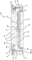
- Fig. 1 shows a partial cross-sectional view of a power semiconductor device 10 according to an embodiment of the invention
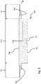
- Fig. 2 shows a vertical cross-section of the power semiconductor device 10 shown in Fig. 1
- the power semiconductor device 10 comprises a disc-shaped first electrode 12a, a disc-shaped second electrode 12b, a wafer 16 sandwiched between the first electrode 12a and the second electrode 12b, an outer insulating ring 24, an inner insulating ring 42, a ring-shaped first flange portion 50, and an O-ring 20.
- a molybdenum layer 70 may be arranged between the wafer 16 and the second electrode 12b as a thermal buffer layer.
- the wafer 16 may be bonded to the molybdenum layer 70, for example by a low temperature bonding process (LTB).
- LTB low temperature bonding process
- the first molybdenum 70 may be free-floating without being bonded to the wafer 16.
- the wafer 16 may be a silicon wafer, for example.
- a switch such as a thyristor, a transistor or a power diode may be implemented in the wafer 16.
- the first electrode 12a has a first contact face 14a and the second electrode 12b has a second contact face 14b opposite to the first contact face 14a.
- the first contact face 14a and the second contact face 14b are both flat and parallel to each other.
- the first contact face 14a and the second contact face 14b may have a circular shape as shown in Fig. 1 .
- the first electrode 12a and the second electrode 12b may act as contact pole pieces.
- the outer insulating ring 24 has the form of a hollow cylinder and may further comprise a fin structure as shown in Figs. 1 and 2 to ensure the necessary clearance and/or creepage distances between the first electrode 12a and the second electrode 12b. As shown in Fig. 2 , the outer insulating ring 24 has an upper first end and a lower second end.
- an upper side of the power semiconductor device 10 is a side of the power semiconductor device 10 where the first contact face 14a is arranged and a lower side of the power semiconductor device 10 is a side of the power semiconductor device 10 where the second contact face 14b is arranged. It is attached with its first end to the first electrode 12a and with its second end to the second electrode 12b.
- the inner insulating ring 42 is laterally arranged inside of the outer insulating ring 24, i.e. the outer insulating ring 24 radially surrounds the inner insulating ring 42, wherein a radial direction R is a direction that is parallel to the first contact face 14a and that extends away from a lateral center of the first contact face 14a. Both, the outer insulating ring 24 and the inner insulating ring 42 are arranged to radially surround the wafer 16.
- the outer insulating ring 24 forms a side wall of a hermetically sealed housing of the power semiconductor device 10.
- Fig. 3 shows a vertical cross-section of the first electrode 12a.
- the first electrode 12a has a main portion 121a and a second flange portion 52 radially extending from an upper end of the main portion 121a.
- the upper end of the first electrode 12a is that end of the first electrode 12a which is in the vertical direction Z at a side where the first contact face 14a is arranged.
- the first electrode 12a On its lower side 18 the first electrode 12a has a recess 15 for receiving a later described spring element 80.
- the first flange portion 50 radially surrounds the main portion 121a of the first electrode 12a.
- Fig. 4 shows a vertical cross-section of the O-ring 20 in a relaxed state, i.e. when no pressure is applied to the O-ring 20 by the inner insulating ring 42 and the first flange portion 50.
- the O-ring 20 In the relaxed state, the O-ring 20 has a cross-section along a plane parallel to the radial direction R and a vertical direction Z perpendicular to the first contact face 14a, which plane is the drawing plane of Fig. 4 .
- the cross-section shown in Fig. 4 is orthogonal to a main axis of the O-ring 20.
- the cross-section is elongated in the vertical direction Z perpendicular to the radial direction R.
- the O-ring 20 has a first width d1 and along the radial direction R the O-ring 20 has a second width d2, which is smaller than the first width d1.
- the first width d1 is the largest width of the O-ring 20 in the vertical cross-section and the second width d2 is the smallest width of the O-ring 20 in the vertical cross-section.
- the O-ring 20 has a cross-section shape that is oval, as shown in the figures.
- the O-ring 20 is made of silicone material.
- the silicone material has good elastic properties and has a sufficient heat resistance to withstand the thermal load during operation of the power semiconductor device.
- the O-ring 20 is made of another resiliently and/or reversibly deformable material.
- the inner insulating ring 42 may be made of a polymer material which has good electrical insulating properties.
- the outer insulating ring 24 may be made of a ceramic material. The inner insulating ring 42 can efficiently shield the outer insulating ring 24 against the arc plasma in case of electrical arcing and prevent explosion of the housing of the power semiconductor device 10 in case of a device failure and electrical arcing.
- the second flange portion 52 is arranged and radially extends on a side of the first flange portion 50 opposite to the O-ring 20.
- the first electrode 12a and the second electrode 12b is made from a material having high electrical conductivity such as copper.
- the second flange portion 52 may be made from copper which is a relatively soft material that may easily be damaged when getting into contact with an arc plasma in case of electrical arcing due to a device failure.
- the first flange portion 50 is made of a material that can withstand high temperatures of an arc plasma in case of electrical arcing. Exemplarily it may be made of steel. In an orthogonal projection onto a plane parallel to the first contact face 14a, the first flange portion 50 overlaps the second flange portion 52 in an area radially extending between the O-ring 20 and the main portion 121a of the first electrode 12a.
- the first flange portion 50 has a first flat surface portion 50a and the second flange portion 52 has a second flat surface portion 52a which is parallel to the first flat surface portion 50a and which is pressed onto the first flat surface portion 50a, wherein in an orthogonal projection onto a plane parallel to the first contact face 14a, the first flat surface portion 50a and the second flat surface portion 52a extend in an area between the O-ring 20 and the first electrode 12a.
- the first flat surface portion 50a is shown to be in direct contact with the second flat surface portion 52a.
- a polymer foil 56 may be sandwiched between the first flat surface portion 50a and the second flat surface portion 52a to provide an additional sealing effect.
- the polymer foil 56 may be a Polytetrafluoroethylene (PTFE) foil. It may exemplarily have a thickness in a range between 50 ⁇ m and 500 ⁇ m.
- PTFE Polytetrafluoroethylene
- the first modified embodiment may be identical to the embodiment illustrated in Figs. 1 and 2 .
- a first portion 50b of the first flange portion 50 is fully overlapped with a second portion 42b of the inner insulating ring 42 in a view along the radial direction R.
- the O-ring 20 is arranged radially outside of the first portion 50b and of the second portion. With the radial overlap of the first portion 50b and the second portion 42b the O-ring 20 is shielded against an arc plasma generated in the power semiconductor device 10 in case of electrical arcing due to a device failure.
- the inner insulating ring 42 has a first end and a second end in the vertical direction Z perpendicular to the radial direction R, wherein the O-ring 20 is arranged on the first end.
- the second end has a radially protruding bottom portion 42a extending radially inwards to the second electrode 12b.
- a rubber protection ring 38 is attached to and surrounds the wafer 16 radially inside of the inner insulating ring 42.
- the bottom portion 42a contacts the rubber protection ring 38 so that a space 60 is defined by the inner insulating ring 42, the first electrode 12a, the rubber protection ring 38 and the first flange portion 50.
- the space may exemplarily be filled with a protection gas such as nitrogen or helium.
- a pressure increase in the housing of the power semiconductor device 10 can be kept at a relatively low level and thereby explosion of the housing can be prevented by providing the space 60.
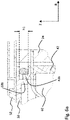
- the power semiconductor device 10 comprises an exchangeable copper insert 85 between the first electrode 12a and the wafer 16.
- exchangeable copper insert 85 the electrical contact area between first electrode 12a and a main contact on the wafer 16 can be adjusted for different wafer diameters. Accordingly, it is possible to use the same housing (including the first electrode 12a, the second electrode 12b, the outer insulating ring 24, the first flange portion 50 and the inner insulating ring 42) also for various chip diameters by respectively using different sized copper inserts.
- a gate lead 90 is guided through a first radial opening 92 in the inner insulating ring 42 and through a second radial opening 94 in the outer insulating ring 24.
- the gate lead 90 is further guided through a channel in the copper insert 85 or in the first electrode 12a or between the copper insert 85 and the first electrode 12a to a control terminal at the lateral center of the wafer 16.
- the copper insert 85 has an opening which is aligned with the above mentioned recess 15 in the first gate electrode 12a for receiving a spring element 80 used for pressing the gate lead 90 or a gate contact connected to the gate lead 90 onto the control terminal of the wafer 16.
- Fig. 5 shows a vertical cross-section of the second electrode 12b included in the power semiconductor device of Fig. 1 . It comprises a main portion 121b and a third flange portion 54 which is radially extending from a lower side of the main portion 121b. The lower side of the main portion 121b forms the second contact face 14b and an upper side 17 of the main portion 121b is electrically connected to the molybdenum layer 70.
- the second electrode 12b is attached to the outer insulating ring 24 with the third flange portion 54.
- Figs. 6a to 6c show respectively a portion of the vertical cross-section of Fig. 2 for different assembling heights due to different wafer thicknesses.
- the different assembling heights result in different compression states of the O-ring 20.
- the O-ring 20 is vertically compressed to a vertical width h1 (relatively low compression state)
- Fig. 6b the O-ring 20 is compressed to a vertical width h2 ⁇ h1 (medium compressed state)
- Fig. 6c the O-ring is compressed to a vertical width h3 ⁇ h2 (strongly compressed state).
- Fig. 8 shows a partial cross-sectional view of a power semiconductor device 10' which is a second modified embodiment of the power semiconductor device 10. The power semiconductor device 10' differs from the power semiconductor device 10 of Fig.
- the bottom portion 42a' of an inner insulating ring 42' extending radially inwards to the second electrode 12b has a different shape than the bottom portion of inner insulating ring 42.
- the bottom portion 42' has a step-like shape in a vertical cross-section.
- the rubber protection ring 38 covers only a side surface and part of a top surface of the wafer 16.
- the rubber protection ring 38 may also cover other parts of a wafer surface, e.g. a lower side of the wafer 16 or only part of the side surface.
- the wafer 16 is described with a control terminal that is connected to the outside via a gate lead 90.
- the wafer 16 may have no control terminal and no gate lead 90 may be provided.
- the outer insulating ring 24 may have no first radial opening 92 and the inner insulating ring 42 may have no second radial opening 94.
- a second molybdenum layer may be arranged as a thermal buffer layer between the wafer 16 and the first electrode 12a.
- the power semiconductor device 10 was described with the exchangeable copper insert 85 arranged between the wafer 16 and the first electrode 12a. However, in another exemplary embodiment no copper insert 85 may be interposed between the first electrode 12a and the wafer 16.
Landscapes
- Die Bonding (AREA)
Claims (14)
- Leistungshalbleitervorrichtung (10), umfassend:eine scheibenförmige erste Elektrode (12a), die eine erste Kontaktfläche (14a) aufweist, und eine scheibenförmige zweite Elektrode (12b), die eine zweite Kontaktfläche (14b) gegenüber der ersten Kontaktfläche (14a) aufweist;einen Wafer (16), der sandwichartig zwischen der ersten Elektrode (12a) und der zweiten Elektrode (12b) angeordnet ist;einen äußeren Isolationsring (24), der an der ersten Elektrode (12a) und an der zweiten Elektrode (12b) angebracht ist, wobei der äußere Isolationsring (24) den Wafer (16) umgibt;einen inneren Isolationsring (42; 42') innerhalb des äußeren Isolationsrings (24) und der den Wafer (16) umgibt;einen ringförmigen ersten Flanschabschnitt (50), der einen Hauptabschnitt (121a) der ersten Elektrode (12a) lateral umgibt, wobei eine radiale erste Richtung (R) parallel zu der ersten Kontaktfläche (14a) ist;einen O-Ring (20), der den Hauptabschnitt (121a) der ersten Elektrode (12a) radial umgibt und in einer zweiten Richtung (Z) senkrecht zu der ersten Kontaktfläche (14a) sandwichartig zwischen dem inneren Isolationsring (42; 42') und dem ersten Flanschabschnitt (50) angeordnet ist,wobei der O-Ring (20) in einem entspannten Zustand einen Querschnitt aufweist, der in einer vertikalen Richtung (Z) senkrecht zu der radialen Richtung (R) derart länglich ist, dass in einem entspannten Zustand eine Höhe des O-Rings in der vertikalen Richtung größer als eine Breite des O-Rings in der radialen Richtung ist, und wobei der O-Ring (20) elastisch reversibel verformbar ist;wobei die erste Elektrode (12a) einen zweiten Flanschabschnitt (52) aufweist, der sich von dem Hauptabschnitt (121a) der ersten Elektrode (12a) auf einer Seite des ersten Flanschabschnitts (50) gegenüber zu dem O-Ring (20) radial erstreckt, wobei der zweite Flanschabschnitt (52) ein integraler Teil der ersten Elektrode (12a) ist; undwobei in einer orthogonalen Projektion auf eine Ebene parallel zu der ersten Kontaktfläche (14a) der erste Flanschabschnitt (50) den zweiten Flanschabschnitt (52) in einem Bereich überlagert, der sich radial zwischen dem O-Ring (20) und dem Hauptabschnitt (121a) der ersten Elektrode (12a) erstreckt.
- Leistungshalbleitervorrichtung (10) nach einem der vorhergehenden Ansprüche, wobei der innere Isolationsring (42; 42') Polymermaterial umfasst.
- Leistungshalbleitervorrichtung (10) nach einem der vorhergehenden Ansprüche, wobei der äußere Isolationsring (24) Keramikmaterial umfasst.
- Leistungshalbleitervorrichtung (10) nach einem der vorhergehenden Ansprüche, wobei die erste Elektrode (12a) und/oder die zweite Elektrode (12b) aus Kupfer bestehen.
- Leistungshalbleitervorrichtung (10) nach einem der vorhergehenden Ansprüche, wobei der erste Flanschabschnitt (50) Stahl umfasst.
- Leistungshalbleitervorrichtung (10) nach Anspruch 1, wobei der zweite Flanschabschnitt (52) Kupfer umfasst.
- Leistungshalbleitervorrichtung (10) nach einem der vorhergehenden Ansprüche, wobei der erste Flanschabschnitt (50) einen ersten flachen Oberflächenabschnitt (50a) aufweist und der zweite Flanschabschnitt (52) einen zweiten flachen Oberflächenabschnitt (52a) aufweist, der parallel zu dem ersten flachen Oberflächenabschnitt (50a) ist und der auf den ersten flachen Oberflächenabschnitt (50a) gedrückt ist, wobei sich in einer orthogonalen Projektion auf eine Ebene parallel zu der ersten Kontaktfläche (14a) der erste flache Oberflächenabschnitt (50a) und der zweite flache Oberflächenabschnitt (52a) in einem Bereich zwischen dem O-Ring (20) und dem Hauptabschnitt (121a) der ersten Elektrode (12a) erstrecken.
- Leistungshalbleitervorrichtung (10) nach Anspruch 7, wobei eine Polymerfolie (56) sandwichartig zwischen dem ersten flachen Oberflächenabschnitt (50a) und dem zweiten flachen Oberflächenabschnitt (52a) angeordnet ist.
- Leistungshalbleitervorrichtung (10) nach einem der vorhergehenden Ansprüche, wobei in einer Ansicht entlang der radialen Richtung (R) ein erster Abschnitt (50b) des ersten Flanschabschnitts (50) vollständig mit einem zweiten Abschnitt (42b) des inneren Isolationsrings (42; 42') überlagert ist und wobei der O-Ring (20) radial außerhalb des ersten Abschnitts (50b) und des zweiten Abschnitts angeordnet ist.
- Leistungshalbleitervorrichtung (10) nach einem der vorhergehenden Ansprüche, umfassend einen austauschbaren Kupfereinsatz (85), der zwischen der ersten Elektrode (12a) und dem Wafer (16) angeordnet ist.
- Leistungshalbleitervorrichtung (10) nach einem der vorhergehenden Ansprüche, wobei der innere Isolationsring (42; 42') ein erstes Ende und ein zweites Ende in der zweiten Richtung (Z) aufweist, wobei der O-Ring (20) an dem ersten Ende angeordnet ist und wobei das zweite Ende einen radial hervorstehenden unteren Abschnitt (42a; 42a') aufweist, der sich radial nach innen zu der zweiten Elektrode (12b) erstreckt.
- Leistungshalbleitervorrichtung (10) nach Anspruch 13, wobei ein Gummischutzring (38) an dem Wafer (16) angebracht ist und den Wafer (16) radial innerhalb des inneren Isolationsrings (42; 42') umgibt, wobei der untere Abschnitt (42; 42a') mit dem Gummischutzring (38) in Kontakt ist.
- Leistungshalbleitervorrichtung (10) nach Anspruch 12, wobei ein Raum (60) durch den inneren Isolationsring (42; 42'), die erste Elektrode (12a), den Gummischutzring (38) und den ersten Flanschabschnitt (50) definiert ist.
- Leistungshalbleitervorrichtung (10) nach einem der vorhergehenden Ansprüche, wobei der Querschnitt des O-Rings (20) eine ovale Form aufweist.
Applications Claiming Priority (2)
| Application Number | Priority Date | Filing Date | Title |
|---|---|---|---|
| EP19189286 | 2019-07-31 | ||
| PCT/EP2020/071387 WO2021018957A1 (en) | 2019-07-31 | 2020-07-29 | Power semiconductor device |
Publications (2)
| Publication Number | Publication Date |
|---|---|
| EP3824497A1 EP3824497A1 (de) | 2021-05-26 |
| EP3824497B1 true EP3824497B1 (de) | 2022-05-04 |
Family
ID=67514362
Family Applications (1)
| Application Number | Title | Priority Date | Filing Date |
|---|---|---|---|
| EP20744076.9A Active EP3824497B1 (de) | 2019-07-31 | 2020-07-29 | Leistungshalbleiterbauelement |
Country Status (5)
| Country | Link |
|---|---|
| US (1) | US12002722B2 (de) |
| EP (1) | EP3824497B1 (de) |
| JP (1) | JP7432072B2 (de) |
| CN (1) | CN114207817B (de) |
| WO (1) | WO2021018957A1 (de) |
Families Citing this family (3)
| Publication number | Priority date | Publication date | Assignee | Title |
|---|---|---|---|---|
| US12463155B2 (en) * | 2021-08-27 | 2025-11-04 | Dynex Semiconductor Limited | Semiconductor device |
| US20230187850A1 (en) * | 2021-12-13 | 2023-06-15 | Intel Corporation | Liquid metal connection device and method |
| EP4471843B1 (de) * | 2023-05-30 | 2025-07-09 | Hitachi Energy Ltd | Halbleiterschaltvorrichtung mit drucksystem |
Citations (2)
| Publication number | Priority date | Publication date | Assignee | Title |
|---|---|---|---|---|
| DE3941041A1 (de) * | 1989-07-31 | 1991-02-07 | Siemens Ag | Anordnung mit einem halbleiterbauelement |
| EP3117455A1 (de) * | 2015-05-19 | 2017-01-18 | ABB Schweiz AG | Halbleiterbauelement |
Family Cites Families (12)
| Publication number | Priority date | Publication date | Assignee | Title |
|---|---|---|---|---|
| JPS5354971A (en) * | 1976-10-28 | 1978-05-18 | Mitsubishi Electric Corp | Semiconductor device |
| US4274106A (en) | 1977-11-07 | 1981-06-16 | Mitsubishi Denki Kabushiki Kaisha | Explosion proof vibration resistant flat package semiconductor device |
| JPS54161272A (en) | 1978-06-09 | 1979-12-20 | Mitsubishi Electric Corp | Flat semiconductor device |
| JPS5635443A (en) | 1979-08-31 | 1981-04-08 | Toshiba Corp | Semiconductor device |
| JPH065686B2 (ja) | 1985-09-04 | 1994-01-19 | 株式会社日立製作所 | 圧接型半導体装置 |
| DE8909244U1 (de) | 1989-07-31 | 1989-09-21 | Siemens AG, 1000 Berlin und 8000 München | Halbleiterbauelement |
| JPH112326A (ja) | 1997-06-11 | 1999-01-06 | Seiko Epson Corp | Oリング及びこれを具備する装置 |
| DE10306767A1 (de) * | 2003-02-18 | 2004-08-26 | eupec Europäische Gesellschaft für Leistungshalbleiter mbH | Halbleitermodul |
| JP5040234B2 (ja) | 2006-09-26 | 2012-10-03 | 三菱電機株式会社 | 圧接型半導体装置 |
| JP2016062983A (ja) | 2014-09-16 | 2016-04-25 | 株式会社東芝 | 半導体装置 |
| EP3007220A1 (de) | 2014-10-10 | 2016-04-13 | ABB Technology AG | Leistungshalbleiterbauelement mit Schutz vor Explosion oder Bruch |
| EP3073530B1 (de) | 2015-03-23 | 2017-05-03 | ABB Schweiz AG | Rückwärtsleitendes hochleistungshalbleiterbauelement |
-
2020
- 2020-07-29 JP JP2022506212A patent/JP7432072B2/ja active Active
- 2020-07-29 WO PCT/EP2020/071387 patent/WO2021018957A1/en not_active Ceased
- 2020-07-29 CN CN202080054574.0A patent/CN114207817B/zh active Active
- 2020-07-29 EP EP20744076.9A patent/EP3824497B1/de active Active
- 2020-07-29 US US17/631,589 patent/US12002722B2/en active Active
Patent Citations (2)
| Publication number | Priority date | Publication date | Assignee | Title |
|---|---|---|---|---|
| DE3941041A1 (de) * | 1989-07-31 | 1991-02-07 | Siemens Ag | Anordnung mit einem halbleiterbauelement |
| EP3117455A1 (de) * | 2015-05-19 | 2017-01-18 | ABB Schweiz AG | Halbleiterbauelement |
Also Published As
| Publication number | Publication date |
|---|---|
| CN114207817A (zh) | 2022-03-18 |
| US12002722B2 (en) | 2024-06-04 |
| US20220336300A1 (en) | 2022-10-20 |
| CN114207817B (zh) | 2023-03-24 |
| JP2022542985A (ja) | 2022-10-07 |
| EP3824497A1 (de) | 2021-05-26 |
| JP7432072B2 (ja) | 2024-02-16 |
| WO2021018957A1 (en) | 2021-02-04 |
Similar Documents
| Publication | Publication Date | Title |
|---|---|---|
| EP1906443B1 (de) | Druckkontakt-Halbleiterbauelement | |
| EP3824497B1 (de) | Leistungshalbleiterbauelement | |
| US4099201A (en) | Semiconductor rectifier assembly having an insulating material therein that evolves gases when exposed to an arc | |
| US3280389A (en) | Freely expanding pressure mounted semiconductor device | |
| EP3117455B1 (de) | Halbleiterbauelement | |
| JP2726222B2 (ja) | カットオフ可能な高出力半導体素子 | |
| US4249034A (en) | Semiconductor package having strengthening and sealing upper chamber | |
| EP3120370B1 (de) | Vorrichtung zur unterbrechung eines stromkreises | |
| KR20160103486A (ko) | 반도체 장치 및 반도체 모듈 | |
| US4956696A (en) | Compression loaded semiconductor device | |
| US3581160A (en) | Semiconductor rectifier assembly having high explosion rating | |
| JP6585569B2 (ja) | 半導体装置 | |
| US4274106A (en) | Explosion proof vibration resistant flat package semiconductor device | |
| US4775916A (en) | Pressure contact semiconductor device | |
| US4150394A (en) | Flat package semiconductor device having high explosion preventing capacity | |
| EP0194946B1 (de) | Statischer Induktionsthyristor mit Doppel-Gate vom Druckkontakttyp | |
| US3885243A (en) | Semiconductor device | |
| WO2015172956A1 (en) | Power semiconductor device | |
| US4329701A (en) | Semiconductor package | |
| CA2940087C (en) | Improved disk cell for several pressure-contacted semiconductor components | |
| EP4143879A1 (de) | Leistungshalbleiterbauelement mit stromumgehungsmechanismus | |
| US3513361A (en) | Flat package electrical device | |
| JPH01128437A (ja) | 電力用半導体素子 | |
| JP3345253B2 (ja) | 圧接型半導体装置 | |
| JP7412876B2 (ja) | 真空開閉装置 |
Legal Events
| Date | Code | Title | Description |
|---|---|---|---|
| STAA | Information on the status of an ep patent application or granted ep patent |
Free format text: STATUS: UNKNOWN |
|
| STAA | Information on the status of an ep patent application or granted ep patent |
Free format text: STATUS: THE INTERNATIONAL PUBLICATION HAS BEEN MADE |
|
| PUAI | Public reference made under article 153(3) epc to a published international application that has entered the european phase |
Free format text: ORIGINAL CODE: 0009012 |
|
| STAA | Information on the status of an ep patent application or granted ep patent |
Free format text: STATUS: REQUEST FOR EXAMINATION WAS MADE |
|
| 17P | Request for examination filed |
Effective date: 20210216 |
|
| AK | Designated contracting states |
Kind code of ref document: A1 Designated state(s): AL AT BE BG CH CY CZ DE DK EE ES FI FR GB GR HR HU IE IS IT LI LT LU LV MC MK MT NL NO PL PT RO RS SE SI SK SM TR |
|
| STAA | Information on the status of an ep patent application or granted ep patent |
Free format text: STATUS: EXAMINATION IS IN PROGRESS |
|
| 17Q | First examination report despatched |
Effective date: 20210609 |
|
| REG | Reference to a national code |
Ref country code: DE Ref legal event code: R079 Ref document number: 602020003056 Country of ref document: DE Free format text: PREVIOUS MAIN CLASS: H01L0025160000 Ipc: H01L0023000000 |
|
| GRAP | Despatch of communication of intention to grant a patent |
Free format text: ORIGINAL CODE: EPIDOSNIGR1 |
|
| STAA | Information on the status of an ep patent application or granted ep patent |
Free format text: STATUS: GRANT OF PATENT IS INTENDED |
|
| RIC1 | Information provided on ipc code assigned before grant |
Ipc: H01L 23/10 20060101ALI20211115BHEP Ipc: H01L 23/051 20060101ALI20211115BHEP Ipc: H01L 23/04 20060101ALI20211115BHEP Ipc: H01L 23/58 20060101ALI20211115BHEP Ipc: H01L 23/62 20060101ALI20211115BHEP Ipc: H01L 23/60 20060101ALI20211115BHEP Ipc: H01L 25/11 20060101ALI20211115BHEP Ipc: H01L 25/16 20060101ALI20211115BHEP Ipc: H01L 23/00 20060101AFI20211115BHEP |
|
| DAV | Request for validation of the european patent (deleted) | ||
| DAX | Request for extension of the european patent (deleted) | ||
| INTG | Intention to grant announced |
Effective date: 20211201 |
|
| RAP3 | Party data changed (applicant data changed or rights of an application transferred) |
Owner name: HITACHI ENERGY SWITZERLAND AG |
|
| GRAS | Grant fee paid |
Free format text: ORIGINAL CODE: EPIDOSNIGR3 |
|
| GRAA | (expected) grant |
Free format text: ORIGINAL CODE: 0009210 |
|
| STAA | Information on the status of an ep patent application or granted ep patent |
Free format text: STATUS: THE PATENT HAS BEEN GRANTED |
|
| AK | Designated contracting states |
Kind code of ref document: B1 Designated state(s): AL AT BE BG CH CY CZ DE DK EE ES FI FR GB GR HR HU IE IS IT LI LT LU LV MC MK MT NL NO PL PT RO RS SE SI SK SM TR |
|
| REG | Reference to a national code |
Ref country code: GB Ref legal event code: FG4D |
|
| REG | Reference to a national code |
Ref country code: CH Ref legal event code: EP |
|
| REG | Reference to a national code |
Ref country code: AT Ref legal event code: REF Ref document number: 1490033 Country of ref document: AT Kind code of ref document: T Effective date: 20220515 |
|
| REG | Reference to a national code |
Ref country code: DE Ref legal event code: R096 Ref document number: 602020003056 Country of ref document: DE |
|
| REG | Reference to a national code |
Ref country code: IE Ref legal event code: FG4D |
|
| REG | Reference to a national code |
Ref country code: LT Ref legal event code: MG9D |
|
| REG | Reference to a national code |
Ref country code: NL Ref legal event code: MP Effective date: 20220504 |
|
| REG | Reference to a national code |
Ref country code: AT Ref legal event code: MK05 Ref document number: 1490033 Country of ref document: AT Kind code of ref document: T Effective date: 20220504 |
|
| PG25 | Lapsed in a contracting state [announced via postgrant information from national office to epo] |
Ref country code: SE Free format text: LAPSE BECAUSE OF FAILURE TO SUBMIT A TRANSLATION OF THE DESCRIPTION OR TO PAY THE FEE WITHIN THE PRESCRIBED TIME-LIMIT Effective date: 20220504 Ref country code: PT Free format text: LAPSE BECAUSE OF FAILURE TO SUBMIT A TRANSLATION OF THE DESCRIPTION OR TO PAY THE FEE WITHIN THE PRESCRIBED TIME-LIMIT Effective date: 20220905 Ref country code: NO Free format text: LAPSE BECAUSE OF FAILURE TO SUBMIT A TRANSLATION OF THE DESCRIPTION OR TO PAY THE FEE WITHIN THE PRESCRIBED TIME-LIMIT Effective date: 20220804 Ref country code: NL Free format text: LAPSE BECAUSE OF FAILURE TO SUBMIT A TRANSLATION OF THE DESCRIPTION OR TO PAY THE FEE WITHIN THE PRESCRIBED TIME-LIMIT Effective date: 20220504 Ref country code: LT Free format text: LAPSE BECAUSE OF FAILURE TO SUBMIT A TRANSLATION OF THE DESCRIPTION OR TO PAY THE FEE WITHIN THE PRESCRIBED TIME-LIMIT Effective date: 20220504 Ref country code: HR Free format text: LAPSE BECAUSE OF FAILURE TO SUBMIT A TRANSLATION OF THE DESCRIPTION OR TO PAY THE FEE WITHIN THE PRESCRIBED TIME-LIMIT Effective date: 20220504 Ref country code: GR Free format text: LAPSE BECAUSE OF FAILURE TO SUBMIT A TRANSLATION OF THE DESCRIPTION OR TO PAY THE FEE WITHIN THE PRESCRIBED TIME-LIMIT Effective date: 20220805 Ref country code: FI Free format text: LAPSE BECAUSE OF FAILURE TO SUBMIT A TRANSLATION OF THE DESCRIPTION OR TO PAY THE FEE WITHIN THE PRESCRIBED TIME-LIMIT Effective date: 20220504 Ref country code: BG Free format text: LAPSE BECAUSE OF FAILURE TO SUBMIT A TRANSLATION OF THE DESCRIPTION OR TO PAY THE FEE WITHIN THE PRESCRIBED TIME-LIMIT Effective date: 20220804 Ref country code: AT Free format text: LAPSE BECAUSE OF FAILURE TO SUBMIT A TRANSLATION OF THE DESCRIPTION OR TO PAY THE FEE WITHIN THE PRESCRIBED TIME-LIMIT Effective date: 20220504 |
|
| PG25 | Lapsed in a contracting state [announced via postgrant information from national office to epo] |
Ref country code: RS Free format text: LAPSE BECAUSE OF FAILURE TO SUBMIT A TRANSLATION OF THE DESCRIPTION OR TO PAY THE FEE WITHIN THE PRESCRIBED TIME-LIMIT Effective date: 20220504 Ref country code: PL Free format text: LAPSE BECAUSE OF FAILURE TO SUBMIT A TRANSLATION OF THE DESCRIPTION OR TO PAY THE FEE WITHIN THE PRESCRIBED TIME-LIMIT Effective date: 20220504 Ref country code: LV Free format text: LAPSE BECAUSE OF FAILURE TO SUBMIT A TRANSLATION OF THE DESCRIPTION OR TO PAY THE FEE WITHIN THE PRESCRIBED TIME-LIMIT Effective date: 20220504 Ref country code: IS Free format text: LAPSE BECAUSE OF FAILURE TO SUBMIT A TRANSLATION OF THE DESCRIPTION OR TO PAY THE FEE WITHIN THE PRESCRIBED TIME-LIMIT Effective date: 20220904 |
|
| PG25 | Lapsed in a contracting state [announced via postgrant information from national office to epo] |
Ref country code: SM Free format text: LAPSE BECAUSE OF FAILURE TO SUBMIT A TRANSLATION OF THE DESCRIPTION OR TO PAY THE FEE WITHIN THE PRESCRIBED TIME-LIMIT Effective date: 20220504 Ref country code: SK Free format text: LAPSE BECAUSE OF FAILURE TO SUBMIT A TRANSLATION OF THE DESCRIPTION OR TO PAY THE FEE WITHIN THE PRESCRIBED TIME-LIMIT Effective date: 20220504 Ref country code: RO Free format text: LAPSE BECAUSE OF FAILURE TO SUBMIT A TRANSLATION OF THE DESCRIPTION OR TO PAY THE FEE WITHIN THE PRESCRIBED TIME-LIMIT Effective date: 20220504 Ref country code: ES Free format text: LAPSE BECAUSE OF FAILURE TO SUBMIT A TRANSLATION OF THE DESCRIPTION OR TO PAY THE FEE WITHIN THE PRESCRIBED TIME-LIMIT Effective date: 20220504 Ref country code: EE Free format text: LAPSE BECAUSE OF FAILURE TO SUBMIT A TRANSLATION OF THE DESCRIPTION OR TO PAY THE FEE WITHIN THE PRESCRIBED TIME-LIMIT Effective date: 20220504 Ref country code: DK Free format text: LAPSE BECAUSE OF FAILURE TO SUBMIT A TRANSLATION OF THE DESCRIPTION OR TO PAY THE FEE WITHIN THE PRESCRIBED TIME-LIMIT Effective date: 20220504 Ref country code: CZ Free format text: LAPSE BECAUSE OF FAILURE TO SUBMIT A TRANSLATION OF THE DESCRIPTION OR TO PAY THE FEE WITHIN THE PRESCRIBED TIME-LIMIT Effective date: 20220504 |
|
| REG | Reference to a national code |
Ref country code: DE Ref legal event code: R097 Ref document number: 602020003056 Country of ref document: DE |
|
| PG25 | Lapsed in a contracting state [announced via postgrant information from national office to epo] |
Ref country code: MC Free format text: LAPSE BECAUSE OF FAILURE TO SUBMIT A TRANSLATION OF THE DESCRIPTION OR TO PAY THE FEE WITHIN THE PRESCRIBED TIME-LIMIT Effective date: 20220504 |
|
| PLBE | No opposition filed within time limit |
Free format text: ORIGINAL CODE: 0009261 |
|
| STAA | Information on the status of an ep patent application or granted ep patent |
Free format text: STATUS: NO OPPOSITION FILED WITHIN TIME LIMIT |
|
| REG | Reference to a national code |
Ref country code: BE Ref legal event code: MM Effective date: 20220731 |
|
| PG25 | Lapsed in a contracting state [announced via postgrant information from national office to epo] |
Ref country code: AL Free format text: LAPSE BECAUSE OF FAILURE TO SUBMIT A TRANSLATION OF THE DESCRIPTION OR TO PAY THE FEE WITHIN THE PRESCRIBED TIME-LIMIT Effective date: 20220504 |
|
| 26N | No opposition filed |
Effective date: 20230207 |
|
| PG25 | Lapsed in a contracting state [announced via postgrant information from national office to epo] |
Ref country code: LU Free format text: LAPSE BECAUSE OF NON-PAYMENT OF DUE FEES Effective date: 20220729 Ref country code: FR Free format text: LAPSE BECAUSE OF NON-PAYMENT OF DUE FEES Effective date: 20220731 |
|
| PG25 | Lapsed in a contracting state [announced via postgrant information from national office to epo] |
Ref country code: SI Free format text: LAPSE BECAUSE OF FAILURE TO SUBMIT A TRANSLATION OF THE DESCRIPTION OR TO PAY THE FEE WITHIN THE PRESCRIBED TIME-LIMIT Effective date: 20220504 Ref country code: BE Free format text: LAPSE BECAUSE OF NON-PAYMENT OF DUE FEES Effective date: 20220731 |
|
| P01 | Opt-out of the competence of the unified patent court (upc) registered |
Effective date: 20230528 |
|
| PG25 | Lapsed in a contracting state [announced via postgrant information from national office to epo] |
Ref country code: IE Free format text: LAPSE BECAUSE OF NON-PAYMENT OF DUE FEES Effective date: 20220729 |
|
| PG25 | Lapsed in a contracting state [announced via postgrant information from national office to epo] |
Ref country code: IT Free format text: LAPSE BECAUSE OF FAILURE TO SUBMIT A TRANSLATION OF THE DESCRIPTION OR TO PAY THE FEE WITHIN THE PRESCRIBED TIME-LIMIT Effective date: 20220504 |
|
| REG | Reference to a national code |
Ref country code: CH Ref legal event code: PL |
|
| REG | Reference to a national code |
Ref country code: DE Ref legal event code: R081 Ref document number: 602020003056 Country of ref document: DE Owner name: HITACHI ENERGY LTD, CH Free format text: FORMER OWNER: HITACHI ENERGY SWITZERLAND AG, BADEN, CH |
|
| PG25 | Lapsed in a contracting state [announced via postgrant information from national office to epo] |
Ref country code: MK Free format text: LAPSE BECAUSE OF FAILURE TO SUBMIT A TRANSLATION OF THE DESCRIPTION OR TO PAY THE FEE WITHIN THE PRESCRIBED TIME-LIMIT Effective date: 20220504 Ref country code: CY Free format text: LAPSE BECAUSE OF FAILURE TO SUBMIT A TRANSLATION OF THE DESCRIPTION OR TO PAY THE FEE WITHIN THE PRESCRIBED TIME-LIMIT Effective date: 20220504 Ref country code: CH Free format text: LAPSE BECAUSE OF NON-PAYMENT OF DUE FEES Effective date: 20230731 |
|
| PG25 | Lapsed in a contracting state [announced via postgrant information from national office to epo] |
Ref country code: HU Free format text: LAPSE BECAUSE OF FAILURE TO SUBMIT A TRANSLATION OF THE DESCRIPTION OR TO PAY THE FEE WITHIN THE PRESCRIBED TIME-LIMIT; INVALID AB INITIO Effective date: 20200729 |
|
| PG25 | Lapsed in a contracting state [announced via postgrant information from national office to epo] |
Ref country code: TR Free format text: LAPSE BECAUSE OF FAILURE TO SUBMIT A TRANSLATION OF THE DESCRIPTION OR TO PAY THE FEE WITHIN THE PRESCRIBED TIME-LIMIT Effective date: 20220504 |
|
| REG | Reference to a national code |
Ref country code: GB Ref legal event code: 732E Free format text: REGISTERED BETWEEN 20240718 AND 20240724 |
|
| PG25 | Lapsed in a contracting state [announced via postgrant information from national office to epo] |
Ref country code: MT Free format text: LAPSE BECAUSE OF FAILURE TO SUBMIT A TRANSLATION OF THE DESCRIPTION OR TO PAY THE FEE WITHIN THE PRESCRIBED TIME-LIMIT Effective date: 20220504 |
|
| PG25 | Lapsed in a contracting state [announced via postgrant information from national office to epo] |
Ref country code: BG Free format text: LAPSE BECAUSE OF FAILURE TO SUBMIT A TRANSLATION OF THE DESCRIPTION OR TO PAY THE FEE WITHIN THE PRESCRIBED TIME-LIMIT Effective date: 20220504 |
|
| PG25 | Lapsed in a contracting state [announced via postgrant information from national office to epo] |
Ref country code: BG Free format text: LAPSE BECAUSE OF FAILURE TO SUBMIT A TRANSLATION OF THE DESCRIPTION OR TO PAY THE FEE WITHIN THE PRESCRIBED TIME-LIMIT Effective date: 20220504 |
|
| REG | Reference to a national code |
Ref country code: DE Ref legal event code: R082 Ref document number: 602020003056 Country of ref document: DE Representative=s name: DENNEMEYER & ASSOCIATES RECHTSANWALTSGESELLSCH, DE |
|
| PGFP | Annual fee paid to national office [announced via postgrant information from national office to epo] |
Ref country code: DE Payment date: 20250722 Year of fee payment: 6 |
|
| PGFP | Annual fee paid to national office [announced via postgrant information from national office to epo] |
Ref country code: GB Payment date: 20250722 Year of fee payment: 6 |
|
| REG | Reference to a national code |
Ref country code: DE Ref legal event code: R079 Ref document number: 602020003056 Country of ref document: DE Free format text: PREVIOUS MAIN CLASS: H01L0023000000 Ipc: H10W0099000000 |