EP1906443B1 - Druckkontakt-Halbleiterbauelement - Google Patents
Druckkontakt-Halbleiterbauelement Download PDFInfo
- Publication number
- EP1906443B1 EP1906443B1 EP07004143.9A EP07004143A EP1906443B1 EP 1906443 B1 EP1906443 B1 EP 1906443B1 EP 07004143 A EP07004143 A EP 07004143A EP 1906443 B1 EP1906443 B1 EP 1906443B1
- Authority
- EP
- European Patent Office
- Prior art keywords
- main electrode
- pressure
- semiconductor device
- flanges
- electrode blocks
- Prior art date
- Legal status (The legal status is an assumption and is not a legal conclusion. Google has not performed a legal analysis and makes no representation as to the accuracy of the status listed.)
- Active
Links
Images


Classifications
-
- H—ELECTRICITY
- H10—SEMICONDUCTOR DEVICES; ELECTRIC SOLID-STATE DEVICES NOT OTHERWISE PROVIDED FOR
- H10W—GENERIC PACKAGES, INTERCONNECTIONS, CONNECTORS OR OTHER CONSTRUCTIONAL DETAILS OF DEVICES COVERED BY CLASS H10
- H10W76/00—Containers; Fillings or auxiliary members therefor; Seals
- H10W76/10—Containers or parts thereof
- H10W76/12—Containers or parts thereof characterised by their shape
- H10W76/13—Containers comprising a conductive base serving as an interconnection
- H10W76/138—Containers comprising a conductive base serving as an interconnection having another interconnection being formed by a cover plate parallel to the conductive base, e.g. sandwich type
-
- H—ELECTRICITY
- H10—SEMICONDUCTOR DEVICES; ELECTRIC SOLID-STATE DEVICES NOT OTHERWISE PROVIDED FOR
- H10W—GENERIC PACKAGES, INTERCONNECTIONS, CONNECTORS OR OTHER CONSTRUCTIONAL DETAILS OF DEVICES COVERED BY CLASS H10
- H10W72/00—Interconnections or connectors in packages
-
- H—ELECTRICITY
- H10—SEMICONDUCTOR DEVICES; ELECTRIC SOLID-STATE DEVICES NOT OTHERWISE PROVIDED FOR
- H10W—GENERIC PACKAGES, INTERCONNECTIONS, CONNECTORS OR OTHER CONSTRUCTIONAL DETAILS OF DEVICES COVERED BY CLASS H10
- H10W90/00—Package configurations
-
- H—ELECTRICITY
- H10—SEMICONDUCTOR DEVICES; ELECTRIC SOLID-STATE DEVICES NOT OTHERWISE PROVIDED FOR
- H10W—GENERIC PACKAGES, INTERCONNECTIONS, CONNECTORS OR OTHER CONSTRUCTIONAL DETAILS OF DEVICES COVERED BY CLASS H10
- H10W76/00—Containers; Fillings or auxiliary members therefor; Seals
- H10W76/60—Seals
Definitions
- the present invention relates to pressure-contact semiconductor devices, in particular, explosion-proof structures of packages therefor.
- EP-A-0 096 266 discloses a disc-like semiconductor cell for pressure-contactable power semiconductor elements.
- the semiconductor cell has a sandwich consisting of a semiconductor chip and two molybdenum discs between two pressure contact discs.
- a cylindrical ring having at its inner side surface a protrusion is serving as package.
- a sealing ring is provided between the pressure contact discs and the protrusion.
- GB-A-1 362 499 describes a disc-shaped semiconductor device having electrodes between which a semiconductor body is mounted.
- the device is provided with an internal varistor body joined to one electrode directly and to the other electrode via a resilient metallic annular member.
- JP 60 103347 A discloses a flat semiconductor device, wherein an accurate positioning between an electrode and a cap is enabled and a complete replacement with an inert gas is possible.
- an insulation ring is L-shaped and is surrounding a semiconductor element.
- US-A-3 739 235 describes a transcalent semiconductor device.
- the device comprises a semiconductor body, wherein electrically insulating means are disposed on a surface of the semiconductor body for protection against external shorting.
- JP 62 090951 A describes a semiconductor element, in which the cost of sealing the element from both end sides of an annular hollow insulator through an elastic resin is reduced.
- an elastic resin is sealed in an air gap to form a structure which can endure a heat cycle, an impact and waterproof.
- Pressure-contact semiconductor devices have been used in various fields of application systems such as inverters for industrial use and drive devices of fans and pumps.
- an excessive short-circuit current such as lightning-surge current may happen to flow, which needs an explosion-proof of a pressure-contact semiconductor device from system protection point of view.
- a semiconductor chip semiconductor substrate
- external electrodes main electrode blocks
- metal flanges attached to the external electrodes to the top and bottom of an external-surrounding insulator (insulating container).
- Two annular partition insulators are interposed, in parallel to each other inside the flanges in the surrounding insulator, across the outer peripheral surfaces of the external electrodes and the inner wall of the surrounding insulator, which prevents arcs, generated at the time of breakage of the semiconductor chip, from blowing out through weak portions such as the flanges to outside the package of the semiconductor device (refer to, for example, Japanese Patent Laid-Open No. 5-259302 , Fig. 1 (Patent Document 1) and Japanese Patent Laid-Open No. 56-35439 , Fig. 2 (Patent Document 2)).
- the annular partition insulators are interposed, in parallel to each other inside the flanges in the surrounding insulator, across the outer peripheral surfaces of the external electrodes and the inner wall of the surrounding insulator, the annular partition insulators are fitted onto the outer peripheral surfaces of the external electrodes and the inner wall of the surrounding insulator, to protect the flanges.
- a structure is required that makes no clearances at fitting portions between the partition insulator and the outer peripheral surfaces of the external electrodes or the inner wall of the surrounding insulator. Since radial centering is necessary in welding the flange, clearances are generally made between the external electrodes and the partition insulators in order to allow tolerance of these parts. For that reason, arcs generated from the semiconductor chip may sometimes reach through the clearances the outside of the device as breaking through the flanges. Therefore, sufficient explosion resistance has not been obtained.
- the present invention is made to solve problems as described above, and an object of the invention is to obtain a pressure-contact semiconductor device that has high reliability and high performance of explosion-proof that suppresses arcs, generated accompanied by breakage of a semiconductor substrate due to a short circuit current or the like, from blowing out from the device package.
- the object is achieved by a pressure-contact semiconductor device according to claim 1.
- a pressure-contact semiconductor device of the present invention includes: a semiconductor substrate having a pair of electrodes each on the front and back sides thereof; a pair of thermal buffer plates and a pair of main electrode blocks, each buffer plate and each electrode block having a flange, being provided opposed to the respective electrodes on the semiconductor substrate such that the substrate is sandwiched therebetween; and an insulating container provided between each flange of the main electrode blocks so as to surround the semiconductor substrate; wherein the pressure-contact semiconductor device is configured such that the semiconductor substrate is sealed in a gastight space created by joining the insulating container to each flange, and O-rings are placed on, and a hollow cylindrical insulator is fitted onto, each electrode-side outer peripheral surface of the main electrode blocks in the gastight space.
- a pressure-contact semiconductor device of the invention is provided with an insulator between a semiconductor substrate and flanges, and with O-rings to eliminate clearances between the semiconductor substrate and each of the flanges. Therefore, the pressure-contact semiconductor device can suppress arcs, generated accompanied by breakage of the semiconductor substrate due to a short circuit current or the like, from blowing out from the device package.
- Fig. 1 is a cross-sectional view illustrating a pressure-contact semiconductor device 100 in Embodiment 1 of the present invention
- Fig. 2 a perspective cross-sectional view illustrating a configuration thereof before assembly.
- a semiconductor substrate 1 for the semiconductor device 100 in which a diode or the like is formed, has an anode and cathode electrodes on a pair of main surfaces: the front and back surfaces of the semiconductor substrate.
- a pair of thermal buffer plates 2 and a pair of main electrode blocks 3 each are disposed on the anode and cathode sides, so that the semiconductor substrate 1 is sandwiched therebetween.
- the semiconductor substrate 1 is provided with a protector 20 made of silicon resin or the like on the outermost peripheral portion thereof.
- a protector 20 made of silicon resin or the like on the outermost peripheral portion thereof.
- molybdenum is used for the thermal buffer plates 2 because the thermal expansion rate of molybdenum is nearly the same as that of silicon.
- the main electrode blocks 3 are made of cupper, which has high electric and thermal conductivity.
- the semiconductor substrate 1 is not fixed between each of the thermal buffer plates 2 and of the main electrode blocks 3 by soldering with a brazing alloy, but is sandwiched in contact with them by mechanical pressing force so as to be electrically connected.
- the main electrode blocks 3 are attached with flanges 4.
- a cylindrical insulating container 5, made of an electrical insulating material such as ceramics, surrounding the lateral side of the semiconductor substrate 1 is provided with flanges 6 on the top and bottom ends of the container.
- the semiconductor device 100 is configured in such a package structure that the semiconductor substrate 1 is enclosed by the main electrode blocks 3 and the insulating container 5 together with the flanges 4 and the flanges 6, in a gastight space sealed by joining the flanges 4 to the flanges 6.
- the flanges 4 and the flanges 6 are made of a nickel-iron alloy.
- a positioning pin 21 or a positioning member 22 is provided between the thermal buffer plates 2 and the main electrode blocks 3 in order for components to be placed in position in the assembly process.
- a gas-replacement pipe 7 is provided extending through the lateral side of the insulating container 5 so that a gas in the gastight space can be replaced with inert gas through the pipe.
- the main electrode blocks 3 each on the anode and cathode sides have first outer peripheral surfaces 31 and second outer peripheral surfaces 32 in the gastight space, both of which diameters are lager than that of the semiconductor substrate 1.
- the first outer peripheral surfaces 31 are formed on the flanges 4 sides of the main electrode blocks 3 and have diameters larger than those of the second outer peripheral surfaces 32.
- Steps 33 formed between the first and second outer peripheral surfaces 31 and 32 of the main electrode blocks 3 clamp an insulator, which is described later, via O-rings.
- the first outer peripheral surfaces 31 are formed in proximity to the inner wall of the insulating container 5, for example, to such an extent that the clearances between each of the surfaces and the wall may be kept sufficient for assembling the main electrode blocks 3 and the insulating container 5.
- O-rings 8 are fitted on the second outer peripheral surfaces 32 of the main electrode blocks 3 so as to be in contact with the steps 33 between the first and second outer peripheral surfaces 31 and 32.
- a hollow cylindrical insulator 9 is fitted across the anode and cathode sides of the second outer peripheral surfaces 32 so that the respective O-rings 8 are pressed against the steps 33 in vertical directions toward the semiconductor substrate 1.
- the insulator 9 is usually made of fluoropolymer such as Tefron TM or polyimide resin that has high rigidity to withstand force from the O-rings 8 and high thermal stability (200 °C or higher).
- the O-rings 8 are preferably made of a thermally stable material such as silicon rubber or fluororubber.
- a through hole (not shown) is formed in the lateral side of the insulator 9 to ensure a path to the semiconductor substrate 1, through which internal gas is replaced through a gas-replacement pipe 7 fitted into the hole.
- the through hole is preferably formed small with a diameter of, for example, about one mm to suppress the amount of arcs blowing out from the insulator 9.
- a plurality of through holes may be formed to disperse the path for the gas.
- the pressure-contact semiconductor device 100 configured as described above is provided with the insulator 9 between the semiconductor substrate 1 and each of the flanges 4 and the flanges 6 to eliminate clearances between each of the main electrode blocks 3 and the insulator 9 by placing the O-rings 8, which can suppress arcs, generated accompanied by breakage of the semiconductor substrate due to a short circuit current or the like, from blowing out from the flanges to outside the device package.
- the above-described configuration eliminates necessity for high dimensional accuracy and for press-fitting of elastic members in the assembly process, which improves workability, allowing the device to be manufactured at low costs.
- a conventional pressure-contact semiconductor device is configured such that elastic members cover flange portions, which involves a relatively large usage of silicon rubber, gas may sometimes be produced in long-term use depending on its use environment.
- gas since use of silicon rubber is limited to the O-rings, the usage can be reduced, which can also suppress gas production.
- Embodiment 1 if the O-rings 8 are fitted onto the main electrode blocks 3 in a twisted state, the O-rings 8 may not remain in predetermined positions, furthermore, slip out from the main electrode blocks 3 in some cases. For that reason, circumferential grooves 34 are formed in the second outer peripheral surfaces 32 of the main electrode blocks 3 as shown in the partial cross-sectional view of Fig. 3 (anode side). By fitting the O-rings 8 into the grooves 34, the O-rings 8 can be fixedly placed in the predetermined positions. Consequently, the O-rings 8 do not slip out from the main electrode blocks 3, which allow a semiconductor device to be configured that has an explosion-proof structure and is easy to assemble.
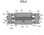
- Fig. 4 is a cross-sectional view illustrating a pressure-contact semiconductor device 101 in Embodiment 3 of the present invention
- Fig. 5 is a perspective cross-sectional view illustrating a configuration thereof before assembly.
- the semiconductor substrate 1 has the anode and cathode electrodes on the pair of main surfaces: the front and back surfaces thereof.
- the pair of thermal buffer plates 2 and the pair of main electrode blocks 3 each are disposed on the anode and cathode sides, so that the semiconductor substrate 1 is sandwiched therebetween.
- the main electrode blocks 3 are attached with the flanges 4 and the cylindrical insulating container 5 made of an insulating material is provided with the flanges 6 on the top and bottom ends thereof.
- the semiconductor device 101 is configured in such a package structure that the semiconductor substrate 1 is enclosed by the main electrode blocks 3 and the insulating container 5 together with the flanges 4 and the flanges 6, in a gastight space sealed by joining the flanges 4 to the flanges 6.
- the gas-replacement pipe 7 is provided extending through the lateral side of the insulating container 5 so that gas in the gastight space can be replaced with inert gas through the pipe.
- the main electrode blocks 3 each on the anode and cathode sides have outer peripheral surfaces 35 in the gastight space, whose diameters are lager than that of the semiconductor substrate 1.
- the O-rings 8 are fitted in grooves 36 formed in the outer peripheral surfaces 35.
- the hollow cylindrical insulator 9 is fitted across each of the outer peripheral surfaces 35: the anode-side and cathode-side surfaces so that the O-rings 8 are clamped between each of the main electrode blocks 3 and the insulator, that is, pressing force are exerted on the O-rings 8 in radial directions by the main electrode blocks 3 and the insulator 9.
- the pressure-contact semiconductor device 101 configured as described above is provided with the insulator 9 between the semiconductor substrate 1 and each of the flanges 4 and the flanges 6 to eliminate clearances between each of the main electrode blocks 3 and the insulator 9 by placing the O-rings 8, which can suppress arcs, generated accompanied by breakage of the semiconductor substrate due to a short circuit current or the like, from blowing out from the flanges 4 and the flanges 6 to outside the device package as with Embodiment 1.
- the above-described configuration eliminates necessity for high dimensional accuracy and for press-fitting of elastic members in the assembly process, which improves workability, allowing the device to be manufactured at low costs as with Embodiment 1.
- a conventional pressure-contact semiconductor device is configured such that elastic members cover flange portions, which involves a relatively large usage of silicon rubber, gas may sometimes be produced in long-term use depending on its use environment.
- gas since use of silicon rubber is limited to the O-rings, the usage can be reduced, which can also suppress gas production.
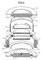
- Fig. 6 is a cross-sectional view illustrating a pressure-contact semiconductor device 102
- Fig. 7 is a perspective cross-sectional view illustrating a configuration thereof before assembly.
- the semiconductor substrate 1 has the anode and cathode electrodes on the pair of main surfaces: the front and back surfaces thereof.
- the pair of thermal buffer plates 2 and the pair of main electrode blocks 3 are each disposed on the anode and cathode sides, so that the semiconductor substrate 1 is sandwiched therebetween.
- the main electrode blocks 3 are attached with the flanges 4 and the cylindrical insulating container 5 made of an insulating material is provided with the flanges 6 on the top and bottom ends thereof.
- the semiconductor device 102 is configured in such a package structure that the semiconductor substrate 1 is enclosed by the main electrode blocks 3 and the insulating container 5 together with the flanges 4 and the flanges 6, in a gastight space sealed by joining the flanges 4 to the flanges 6.
- the gas-replacement pipe 7 is provided extending through the lateral side of the insulating container 5 so that gas in the gastight space can be replaced with inert gas through the pipe.
- elastic members 10 each are additionally provided for covering the anode and cathode sides of the flanges 4 and the flanges 6, and rings 11 are also provided supported on inner peripheries of the elastic members 10 and the outer peripheries of the thermal buffer plates 2 opposed thereto.
- the elastic members 10 suppress arcs from breaking through the flanges 4 and the flanges 6 by covering them when the semiconductor substrate 1 is overloaded. For that reason, silicon rubber, fluororubber, or the like, which has high thermal stability (200 °C or higher), is used for the elastic members 10.
- the rings 11 are disposed between the elastic members 10 and the main electrode blocks 3 so that clearances are filled therewith, which are necessary for assembly, and are further configured to seal the inside by its elastic force. Consequently, the rings 11 suppress arcs from passing through the clearances between the elastic members 10 and the main electrode blocks 3. Therefore, the rings 11 are preferably made of a metal material of high thermal resistance and rigidity such as iron or copper.
- the assembly proceeds to the anode-side configuration, an assembly process for which is in the order almost reverse to those for the anode side;
- the elastic members 10 when the semiconductor substrate 1 is overloaded, the elastic members 10 suppress arcs from directly breaking through the flanges 4 and the flanges 6. At the same time, even if arcs pass through clearances D2 between the elastic members 10 and the main electrode blocks 3 and reach the flanges 4 and the flanges 6, the rings 11 can also suppress the arcs from breaking through the flanges 4 and the flanges 6.
- the above-described configuration can basically be configured by adding the rings 10 to a conventional pressure-contact semiconductor device, it is easy to modify from conventional ones, but yet able to demonstrate high explosion-proof performance.
- Fig. 8 is a partial cross-sectional view illustrating a configuration in which a hollow cylindrical insulating resin 12 is disposed on the inner wall of the insulating container 5.
- the insulating resin 12 is clamped by the cathode and anode sides of the elastic members 10 opposing each other.
- a pressure-contact semiconductor device configured as described above can prevent arcs from directly hitting the insulating container 5 when the semiconductor substrate 1 is overloaded. Consequently, the pressure-contact semiconductor device can be configured to demonstrate higher explosion resistance than that of Embodiment 1.
- projecting portions 17 may be formed on the elastic members 10 at portions thereof contacting the respective rings 11 as shown by the cross-sectional views in Figs. 9A and 9B .
- contact pressure on the rings 11 can be adjusted by varying the width of the projecting portions 17 formed on the elastic members 10, which can prevent the main electrode blocks 3 from being distorted.
- the projecting portions 17 are formed on the elastic members 10 for preventing the distortion of the main electrode blocks 3 .
- Projecting portions 18 may be formed, in contrast, on the rings 11 at portions thereof contacting the elastic members 10 as shown by the cross-sectional views in Figs. 10A and 10B .
- contact pressure on the elastic members 10 can be adjusted by varying the width o,f the projecting portions 18 formed on the rings 11, which can also prevent the main electrode blocks 3 from being distorted as with the third example
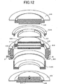
- Fig. 11 is a cross-sectional view illustrating a pressure-contact semiconductor device 103
- Fig. 12 is a perspective cross-sectional view illustrating a configuration thereof before assembly.
- the semiconductor substrate 1 has the anode and cathode electrodes on the pair of main surfaces: the front and back surfaces thereof.
- the pair of thermal buffer plates 2 and the pair of main electrode blocks 3 each are disposed on the anode and cathode sides, so that the semiconductor substrate 1 is sandwiched therebetween.
- the main electrode blocks 3 are attached with the flanges 4 and the cylindrical insulating container 5 made of an insulating material has the flanges 6 on the top and bottom ends thereof.
- the semiconductor device 103 is configured in such a package structure that the semiconductor substrate 1 is enclosed by the main electrode blocks 3 and the insulating container 5 together with the flanges 4 and the flanges 6, in a gastight space sealed by joining the flanges 4 to the flanges 6.
- the gas-replacement pipe 7 is provided extending through the lateral side of the insulating container 5 so that gas in the gastight space can be replaced with inert gas through the pipe.
- elastic members 13 are additionally provided each on the anode and cathode sides in contact with outer peripheries of the main electrode blocks 3 and the inner wall of the insulating container 5, for covering the anode and cathode sides of the flanges 4 and the flanges 6.
- the electrode blocks 3 have diameters different from each other at the outer peripheries contacting the elastic members 13 and one of the diameters on the anode side is larger than that on the cathode side.
- a cathode-side distance D4 between an cathode-side outer periphery and the inner wall of the insulating container 5 is large and an anode-side distance D3 between an anode-side outer periphery and the inner wall of the insulating container 5 is small, which differences, as a matter of course, are reflected on the sizes of press-fitted elastic member 13A and elastic member 13K.
- the elastic members 13 covering the flanges 4 are press-fitted between each of the outer peripheries of the main electrode blocks 3 and the inner periphery of the insulating container 5 so that no clearance is created therebetween. Consequently, when the semiconductor substrate 1 is overloaded, the elastic members 13 can prevent arcs from reaching the flanges 4 and the flanges 6, and can accordingly prevent the arcs from breaking through the flanges 4 and the flanges 6. For that purpose, a machining process such as grinding or abrading is necessary for improving dimensional accuracy of the insulating container 5, the main electrode blocks 3, and the like, which has been a problem with conventional configurations. However, by varying widths of the cathode and anode sides of the elastic member 13K and the elastic member 13A, respectively, it is possible to make the assembly easier as compared to the conventional configurations, allowing the device to be manufactured at low costs.
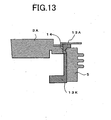
- the anode-side elastic member 13A is formed small in width as shown in Fig. 11 in the fifth example, the main electrode block 3A may not be press-fitted yet in some cases.
- a circumferential groove 14 in a press-fitted portion of the elastic member 13A contacting the outer periphery of the main electrode block 3A or the inner periphery of the insulating container 5 as shown in Fig. 13 , it is possible to reduce and adjust friction force generated at the time of the press-fitting, bringing about improvement of assembly.
- any of the embodiments and Examples described above is characterized in that gastight space structures thereof in a pressure-contact semiconductor device having a package structure in which a semiconductor substrate is sealed in a gastight space by main electrode blocks and an insulating container together with their flanges.
- a pressure-contact semiconductor device further including fin electrodes each contacted with the anode and cathode sides of the main electrode blocks.
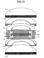
- Fig. 14 is a cross-sectional view of a pressure-contact semiconductor device 104 in Embodiment 10 of the present invention
- Fig. 15 is a perspective cross-sectional view illustrating the pressure-contact semiconductor device 104 before the fin electrodes are attached thereto.
- a pressure-contact semiconductor portion 200 inside which an explosion-proof structure is not necessarily employed, is provided with fin electrodes 15, each being in contact with the anode and cathode sides of main electrode blocks, to press the pressure-contact semiconductor portion 200.
- Elastic members 16 each are sandwiched between the fin electrodes 15 and flanges attached to the semiconductor portion 200.
- the elastic members 16 are made of silicon rubber, fluororubber, or the like having high thermal stability (200 °C or higher).
- the elastic members 16 cover the flanges from their outside and the flanges are closely contacted with the elastic members 16 with pressure by the fin electrodes 15. Thereby, even if arcs break through the flanges when the semiconductor substrate is overloaded, the arcs can be prevented from reaching the outside.
- a pressure-contact semiconductor device can be configured with explosion-proof structure at low-costs even if it is assembled by providing the fin electrodes 15 and the elastic members 16.
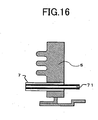
- the gas-replacement pipe 7 is provided. Arcs generated from the semiconductor substrate 1 might leak out through the gas-replacement pipe 7. Hence, a second gas-replacement pipe 71 is provided as being inserted into the gas-replacement pipe 7 as shown in Fig. 16 . Thereby, a path becomes long through which arcs flow round, which results in that a pressure-contact semiconductor device can be configured that has higher explosion resistance.
Landscapes
- Die Bonding (AREA)
Claims (6)
- Druckkontakt-Halbleitervorrichtung, aufweisend:ein Halbleitersubstrat (1) mit einem Paar Elektroden auf einer Vorderseite bzw. einer Rückseite davonein Paar Wärmepufferplatten (2) und ein Paar Hauptelektrodenblöcke (3), wobei jeder Hauptelektrodenblock mit einem Flansch (4) befestigt ist, gegenüberliegend von den entsprechenden Elektroden auf dem Halbleitersubstrat (1) vorgesehen ist, so dass das Substrat sandwichartig dazwischen angeordnet ist;und einen hohlen Isolierbehälter (5), der zwischen den Flanschen (4) der Hauptelektrodenblöcke (3) vorgesehen ist, das Halbleitersubstrat so umgebend, dass das Halbleitersubstrat (1) in einem gasdichten Raum abgedichtet ist, der durch Verbinden des hohlen Isolierbehälters (5) mit den Flanschen (4) erzeugt wird,O-Ringe (8) die jeweils an eine Außenumfangsfläche (32) in dem gasdichten Raum jedes Hauptelektrodenblocks angepasst sind; undeinen hohlzylindrischen Isolator (9) der auf den Außenumfangsflächen (32) in dem gasdichten Raum der Hauptelektrodenblöcke angebracht ist, um das Halbleitersubstrat von den Flanschen und dem hohlen Isolierbehälter abzuschirmen im Zusammenwirken mit den Hauptelektrodenblöcken und den O-Ringen.
- Druckkontakt-Halbleitervorrichtung nach Anspruch 1,
dadurch gekennzeichnet, dass
Umfangsnuten in den Außenumfangsflächen der Hauptelektrodenblöcke ausgebildet sind, und die O-Ringe in die Nuten eingepasst sind. - Druckkontakt-Halbleitervorrichtung nach einem der Ansprüche 1 oder 2,
dadurch gekennzeichnet, dass
ein erstes Gasaustauschrohr (7) vorgesehen ist, das durch den hohlen Isolierbehälter hindurch geführt ist, und ein Durchgangsloch in der Seitenwand des hohlzylindrischen Isolators (9) vorgesehen ist. - Druckkontakt-Halbleitervorrichtung nach Anspruch 3,
dadurch gekennzeichnet, dass
ein zweites Gasaustauschrohr (71) aus einem isolierenden Material in das erste Gasaustauschrohr (7) eingesetzt ist. - Druckkontakt-Halbleitervorrichtung nach einem der Ansprüche 1 bis 4,
dadurch gekennzeichnet, dass
der hohle Isolierbehälter (5) aus Keramik hergestellt ist. - Druckkontakt-Halbleitervorrichtung nach Anspruch 5,
dadurch gekennzeichnet, dass
der hohlzylindrische Isolator (9) aus Fluorpolymer oder Polyimid-Harz hergestellt ist.
Applications Claiming Priority (1)
| Application Number | Priority Date | Filing Date | Title |
|---|---|---|---|
| JP2006260422A JP5040234B2 (ja) | 2006-09-26 | 2006-09-26 | 圧接型半導体装置 |
Publications (3)
| Publication Number | Publication Date |
|---|---|
| EP1906443A2 EP1906443A2 (de) | 2008-04-02 |
| EP1906443A3 EP1906443A3 (de) | 2008-12-03 |
| EP1906443B1 true EP1906443B1 (de) | 2013-09-18 |
Family
ID=38066505
Family Applications (1)
| Application Number | Title | Priority Date | Filing Date |
|---|---|---|---|
| EP07004143.9A Active EP1906443B1 (de) | 2006-09-26 | 2007-02-28 | Druckkontakt-Halbleiterbauelement |
Country Status (3)
| Country | Link |
|---|---|
| US (1) | US8456001B2 (de) |
| EP (1) | EP1906443B1 (de) |
| JP (1) | JP5040234B2 (de) |
Families Citing this family (17)
| Publication number | Priority date | Publication date | Assignee | Title |
|---|---|---|---|---|
| DE102008058189A1 (de) * | 2008-11-20 | 2010-07-22 | Semikron Elektronik Gmbh & Co. Kg | Feuchtigkeitsdichtes Leistungshalbleitermodul mit Zentriereinrichtung |
| DE102009034138B4 (de) * | 2009-07-22 | 2011-06-01 | Semikron Elektronik Gmbh & Co. Kg | Leistungshalbleitermodul mit einem Sandwich mit einem Leistungshalbleiterbauelement |
| WO2012146655A1 (en) | 2011-04-27 | 2012-11-01 | Biom'up | Hemostatic compositions |
| JP2016062983A (ja) * | 2014-09-16 | 2016-04-25 | 株式会社東芝 | 半導体装置 |
| JP6301857B2 (ja) * | 2015-02-24 | 2018-03-28 | 株式会社東芝 | 半導体モジュール |
| DE202015102948U1 (de) | 2015-06-08 | 2015-06-24 | Abb Technology Ag | Halbleiterbauelement |
| JP6359573B2 (ja) | 2016-01-19 | 2018-07-18 | 株式会社東芝 | 半導体装置 |
| DE102016209577A1 (de) * | 2016-06-01 | 2017-12-07 | Siemens Aktiengesellschaft | Leistungsmodul |
| JP6585569B2 (ja) | 2016-09-15 | 2019-10-02 | 株式会社東芝 | 半導体装置 |
| CN110383463B (zh) * | 2017-01-17 | 2023-05-02 | 日立能源瑞士股份公司 | 半导体开关器件 |
| JP6868322B2 (ja) * | 2017-08-31 | 2021-05-12 | 東芝三菱電機産業システム株式会社 | 電力変換装置 |
| EP3824497B1 (de) * | 2019-07-31 | 2022-05-04 | Hitachi Energy Switzerland AG | Leistungshalbleiterbauelement |
| JP7444529B2 (ja) * | 2021-05-17 | 2024-03-06 | 東芝三菱電機産業システム株式会社 | 電力変換装置 |
| EP4162524A1 (de) * | 2021-08-27 | 2023-04-12 | Dynex Semiconductor Limited | Halbleiterbauelement mit fehlerschutzstruktur |
| JP2024055514A (ja) * | 2022-10-07 | 2024-04-18 | 東芝三菱電機産業システム株式会社 | 半導体素子の積層構造体 |
| US20250075795A1 (en) * | 2023-08-28 | 2025-03-06 | Applied Materials, Inc. | Seal assembly with a retaining mechanism |
| WO2025131269A1 (en) * | 2023-12-20 | 2025-06-26 | Hitachi Energy Ltd. | Power semiconductor module |
Family Cites Families (28)
| Publication number | Priority date | Publication date | Assignee | Title |
|---|---|---|---|---|
| GB1362499A (en) | 1971-10-22 | 1974-08-07 | Gen Electric | Semiconductor devices |
| US3739235A (en) | 1972-01-31 | 1973-06-12 | Rca Corp | Transcalent semiconductor device |
| JPS5261962A (en) * | 1975-11-18 | 1977-05-21 | Toshiba Corp | Semiconductor device |
| US4131905A (en) * | 1977-05-26 | 1978-12-26 | Electric Power Research Institute, Inc. | Light-triggered thyristor and package therefore |
| JPS548975A (en) | 1977-06-23 | 1979-01-23 | Mitsubishi Electric Corp | Semiconuctor device |
| US4257058A (en) * | 1979-07-05 | 1981-03-17 | Electric Power Research Institute, Inc. | Package for radiation triggered semiconductor device and method |
| JPS6043016B2 (ja) | 1979-08-31 | 1985-09-26 | 株式会社東芝 | 半導体装置 |
| JPS5635443A (en) * | 1979-08-31 | 1981-04-08 | Toshiba Corp | Semiconductor device |
| JPS5683951A (en) * | 1979-12-12 | 1981-07-08 | Mitsubishi Electric Corp | Semiconductor device |
| JPS56131955A (en) * | 1980-09-01 | 1981-10-15 | Hitachi Ltd | Semiconductor device |
| JPS5750439A (en) * | 1980-09-12 | 1982-03-24 | Hitachi Ltd | Semiconductor device |
| JPS5874351A (ja) | 1981-10-30 | 1983-05-04 | 東レ株式会社 | 銅蒸着ポリエステルフイルム |
| JPS5874351U (ja) * | 1981-11-13 | 1983-05-19 | 株式会社明電舎 | 半導体装置における素子のゲ−ト引き出し構造 |
| DE3221794A1 (de) | 1982-06-09 | 1983-12-15 | Brown, Boveri & Cie Ag, 6800 Mannheim | Scheibenfoermige halbleiterzelle fuer druckkontaktierbare leistungshalbleiterbauelemente |
| JPS60103647A (ja) * | 1983-11-10 | 1985-06-07 | Fuji Electric Co Ltd | 平形半導体装置 |
| JPS60103347A (ja) | 1983-11-11 | 1985-06-07 | Seiko Epson Corp | 合成樹脂製フオトクロミツクレンズ |
| JPS60194565A (ja) * | 1984-03-15 | 1985-10-03 | Mitsubishi Electric Corp | 半導体装置 |
| JPS61125143A (ja) | 1984-11-22 | 1986-06-12 | Toshiba Corp | 半導体装置 |
| JPS6290951A (ja) | 1985-10-16 | 1987-04-25 | Mitsubishi Electric Corp | 半導体装置 |
| JP2529359B2 (ja) * | 1988-08-24 | 1996-08-28 | 松下電器産業株式会社 | グリ―ンシ―トのプレス加工法 |
| JPH0760893B2 (ja) * | 1989-11-06 | 1995-06-28 | 三菱電機株式会社 | 半導体装置およびその製造方法 |
| JPH04352457A (ja) * | 1991-05-30 | 1992-12-07 | Mitsubishi Electric Corp | 圧接型半導体装置及びその製造方法 |
| JPH05259302A (ja) | 1992-03-12 | 1993-10-08 | Fuji Electric Co Ltd | 平形半導体装置のパッケージ構造 |
| DE4227063A1 (de) * | 1992-08-15 | 1994-02-17 | Abb Research Ltd | Abschaltbares Hochleistungs-Halbleiterbauelement |
| JP3010614B2 (ja) * | 1992-12-08 | 2000-02-21 | 富士電機株式会社 | 平形半導体整流素子の取付け構造 |
| DE10306767A1 (de) * | 2003-02-18 | 2004-08-26 | eupec Europäische Gesellschaft für Leistungshalbleiter mbH | Halbleitermodul |
| DE10325517A1 (de) * | 2003-06-05 | 2004-12-23 | Hew-Kabel/Cdt Gmbh & Co. Kg | Elektrische Heizleitung oder Heizband |
| JP5100022B2 (ja) * | 2005-04-08 | 2012-12-19 | 三洋電機株式会社 | 燃料電池システム |
-
2006
- 2006-09-26 JP JP2006260422A patent/JP5040234B2/ja active Active
-
2007
- 2007-02-28 EP EP07004143.9A patent/EP1906443B1/de active Active
- 2007-03-09 US US11/684,140 patent/US8456001B2/en active Active
Also Published As
| Publication number | Publication date |
|---|---|
| JP5040234B2 (ja) | 2012-10-03 |
| EP1906443A3 (de) | 2008-12-03 |
| EP1906443A2 (de) | 2008-04-02 |
| US8456001B2 (en) | 2013-06-04 |
| JP2008084926A (ja) | 2008-04-10 |
| US20080073767A1 (en) | 2008-03-27 |
Similar Documents
| Publication | Publication Date | Title |
|---|---|---|
| EP1906443B1 (de) | Druckkontakt-Halbleiterbauelement | |
| US3280389A (en) | Freely expanding pressure mounted semiconductor device | |
| US10192800B2 (en) | Semiconductor device | |
| JP6102688B2 (ja) | 蓄電装置 | |
| JP6585569B2 (ja) | 半導体装置 | |
| JP6296153B2 (ja) | 蓄電装置 | |
| US10032760B2 (en) | Semiconductor device | |
| JP5965377B2 (ja) | 電流遮断装置とそれを用いた蓄電装置 | |
| KR101941350B1 (ko) | 2 차 배터리 및 2 차 배터리의 제조 방법 | |
| EP3824497B1 (de) | Leistungshalbleiterbauelement | |
| KR20220115993A (ko) | 커버 플레이트 어셈블리, 배터리, 배터리 모듈, 파워 배터리 팩 및 전기 차량 | |
| KR101846685B1 (ko) | 열전모듈 패키징방법 | |
| JP6176338B2 (ja) | 蓄電装置 | |
| JP2000260421A (ja) | 電池の感圧電路遮断機構 | |
| CN119920771B (zh) | 芯片的封装结构和半导体器件 | |
| JP2016004704A (ja) | 蓄電装置 | |
| JPS62128548A (ja) | 半導体装置 | |
| JP2002110311A (ja) | サージアブソーバ及びその製造方法 | |
| JPH02220452A (ja) | 半導体装置 | |
| JPH10247720A (ja) | 圧接型半導体装置 |
Legal Events
| Date | Code | Title | Description |
|---|---|---|---|
| PUAI | Public reference made under article 153(3) epc to a published international application that has entered the european phase |
Free format text: ORIGINAL CODE: 0009012 |
|
| AK | Designated contracting states |
Kind code of ref document: A2 Designated state(s): AT BE BG CH CY CZ DE DK EE ES FI FR GB GR HU IE IS IT LI LT LU LV MC NL PL PT RO SE SI SK TR |
|
| AX | Request for extension of the european patent |
Extension state: AL BA HR MK YU |
|
| PUAL | Search report despatched |
Free format text: ORIGINAL CODE: 0009013 |
|
| AK | Designated contracting states |
Kind code of ref document: A3 Designated state(s): AT BE BG CH CY CZ DE DK EE ES FI FR GB GR HU IE IS IT LI LT LU LV MC NL PL PT RO SE SI SK TR |
|
| AX | Request for extension of the european patent |
Extension state: AL BA HR MK RS |
|
| 17P | Request for examination filed |
Effective date: 20090603 |
|
| AKX | Designation fees paid |
Designated state(s): CH DE LI |
|
| GRAP | Despatch of communication of intention to grant a patent |
Free format text: ORIGINAL CODE: EPIDOSNIGR1 |
|
| INTG | Intention to grant announced |
Effective date: 20130425 |
|
| GRAS | Grant fee paid |
Free format text: ORIGINAL CODE: EPIDOSNIGR3 |
|
| GRAA | (expected) grant |
Free format text: ORIGINAL CODE: 0009210 |
|
| AK | Designated contracting states |
Kind code of ref document: B1 Designated state(s): CH DE LI |
|
| REG | Reference to a national code |
Ref country code: CH Ref legal event code: EP |
|
| REG | Reference to a national code |
Ref country code: CH Ref legal event code: NV Representative=s name: R. A. EGLI AND CO. PATENTANWAELTE, CH |
|
| REG | Reference to a national code |
Ref country code: DE Ref legal event code: R096 Ref document number: 602007032886 Country of ref document: DE Effective date: 20131114 |
|
| REG | Reference to a national code |
Ref country code: DE Ref legal event code: R097 Ref document number: 602007032886 Country of ref document: DE |
|
| PLBE | No opposition filed within time limit |
Free format text: ORIGINAL CODE: 0009261 |
|
| STAA | Information on the status of an ep patent application or granted ep patent |
Free format text: STATUS: NO OPPOSITION FILED WITHIN TIME LIMIT |
|
| 26N | No opposition filed |
Effective date: 20140619 |
|
| REG | Reference to a national code |
Ref country code: DE Ref legal event code: R097 Ref document number: 602007032886 Country of ref document: DE Effective date: 20140619 |
|
| REG | Reference to a national code |
Ref country code: DE Ref legal event code: R084 Ref document number: 602007032886 Country of ref document: DE |
|
| PGFP | Annual fee paid to national office [announced via postgrant information from national office to epo] |
Ref country code: CH Payment date: 20170214 Year of fee payment: 11 |
|
| REG | Reference to a national code |
Ref country code: CH Ref legal event code: PL |
|
| PG25 | Lapsed in a contracting state [announced via postgrant information from national office to epo] |
Ref country code: LI Free format text: LAPSE BECAUSE OF NON-PAYMENT OF DUE FEES Effective date: 20180228 Ref country code: CH Free format text: LAPSE BECAUSE OF NON-PAYMENT OF DUE FEES Effective date: 20180228 |
|
| P01 | Opt-out of the competence of the unified patent court (upc) registered |
Effective date: 20230512 |
|
| REG | Reference to a national code |
Ref country code: DE Ref legal event code: R079 Ref document number: 602007032886 Country of ref document: DE Free format text: PREVIOUS MAIN CLASS: H01L0023051000 Ipc: H10W0076138000 |
|
| PGFP | Annual fee paid to national office [announced via postgrant information from national office to epo] |
Ref country code: DE Payment date: 20260102 Year of fee payment: 20 |