EP3826072A1 - Elektronengas-transistor, monoblock-vorrichtung, die mindestens zwei transistoren in kaskadenschaltung umfasst, und entsprechendes herstellungsverfahren - Google Patents
Elektronengas-transistor, monoblock-vorrichtung, die mindestens zwei transistoren in kaskadenschaltung umfasst, und entsprechendes herstellungsverfahren Download PDFInfo
- Publication number
- EP3826072A1 EP3826072A1 EP20208298.8A EP20208298A EP3826072A1 EP 3826072 A1 EP3826072 A1 EP 3826072A1 EP 20208298 A EP20208298 A EP 20208298A EP 3826072 A1 EP3826072 A1 EP 3826072A1
- Authority
- EP
- European Patent Office
- Prior art keywords
- layer
- trench
- semiconductor layer
- etching
- metallic
- Prior art date
- Legal status (The legal status is an assumption and is not a legal conclusion. Google has not performed a legal analysis and makes no representation as to the accuracy of the status listed.)
- Pending
Links
Images






Classifications
-
- H—ELECTRICITY
- H10—SEMICONDUCTOR DEVICES; ELECTRIC SOLID-STATE DEVICES NOT OTHERWISE PROVIDED FOR
- H10D—INORGANIC ELECTRIC SEMICONDUCTOR DEVICES
- H10D30/00—Field-effect transistors [FET]
- H10D30/60—Insulated-gate field-effect transistors [IGFET]
-
- H—ELECTRICITY
- H10—SEMICONDUCTOR DEVICES; ELECTRIC SOLID-STATE DEVICES NOT OTHERWISE PROVIDED FOR
- H10D—INORGANIC ELECTRIC SEMICONDUCTOR DEVICES
- H10D30/00—Field-effect transistors [FET]
- H10D30/40—FETs having zero-dimensional [0D], one-dimensional [1D] or two-dimensional [2D] charge carrier gas channels
- H10D30/47—FETs having zero-dimensional [0D], one-dimensional [1D] or two-dimensional [2D] charge carrier gas channels having two-dimensional [2D] charge carrier gas channels, e.g. nanoribbon FETs or high electron mobility transistors [HEMT]
- H10D30/471—High electron mobility transistors [HEMT] or high hole mobility transistors [HHMT]
- H10D30/475—High electron mobility transistors [HEMT] or high hole mobility transistors [HHMT] having wider bandgap layer formed on top of lower bandgap active layer, e.g. undoped barrier HEMTs such as i-AlGaN/GaN HEMTs
-
- H—ELECTRICITY
- H10—SEMICONDUCTOR DEVICES; ELECTRIC SOLID-STATE DEVICES NOT OTHERWISE PROVIDED FOR
- H10D—INORGANIC ELECTRIC SEMICONDUCTOR DEVICES
- H10D30/00—Field-effect transistors [FET]
- H10D30/01—Manufacture or treatment
- H10D30/015—Manufacture or treatment of FETs having heterojunction interface channels or heterojunction gate electrodes, e.g. HEMT
-
- H—ELECTRICITY
- H10—SEMICONDUCTOR DEVICES; ELECTRIC SOLID-STATE DEVICES NOT OTHERWISE PROVIDED FOR
- H10D—INORGANIC ELECTRIC SEMICONDUCTOR DEVICES
- H10D30/00—Field-effect transistors [FET]
- H10D30/01—Manufacture or treatment
- H10D30/021—Manufacture or treatment of FETs having insulated gates [IGFET]
-
- H—ELECTRICITY
- H10—SEMICONDUCTOR DEVICES; ELECTRIC SOLID-STATE DEVICES NOT OTHERWISE PROVIDED FOR
- H10D—INORGANIC ELECTRIC SEMICONDUCTOR DEVICES
- H10D62/00—Semiconductor bodies, or regions thereof, of devices having potential barriers
- H10D62/80—Semiconductor bodies, or regions thereof, of devices having potential barriers characterised by the materials
- H10D62/85—Semiconductor bodies, or regions thereof, of devices having potential barriers characterised by the materials being Group III-V materials, e.g. GaAs
- H10D62/8503—Nitride Group III-V materials, e.g. AlN or GaN
-
- H—ELECTRICITY
- H10—SEMICONDUCTOR DEVICES; ELECTRIC SOLID-STATE DEVICES NOT OTHERWISE PROVIDED FOR
- H10D—INORGANIC ELECTRIC SEMICONDUCTOR DEVICES
- H10D62/00—Semiconductor bodies, or regions thereof, of devices having potential barriers
- H10D62/80—Semiconductor bodies, or regions thereof, of devices having potential barriers characterised by the materials
- H10D62/85—Semiconductor bodies, or regions thereof, of devices having potential barriers characterised by the materials being Group III-V materials, e.g. GaAs
- H10D62/854—Semiconductor bodies, or regions thereof, of devices having potential barriers characterised by the materials being Group III-V materials, e.g. GaAs further characterised by the dopants
-
- H—ELECTRICITY
- H10—SEMICONDUCTOR DEVICES; ELECTRIC SOLID-STATE DEVICES NOT OTHERWISE PROVIDED FOR
- H10D—INORGANIC ELECTRIC SEMICONDUCTOR DEVICES
- H10D64/00—Electrodes of devices having potential barriers
- H10D64/20—Electrodes characterised by their shapes, relative sizes or dispositions
- H10D64/23—Electrodes carrying the current to be rectified, amplified, oscillated or switched, e.g. sources, drains, anodes or cathodes
- H10D64/251—Source or drain electrodes for field-effect devices
- H10D64/256—Source or drain electrodes for field-effect devices for lateral devices wherein the source or drain electrodes are recessed in semiconductor bodies
-
- H—ELECTRICITY
- H10—SEMICONDUCTOR DEVICES; ELECTRIC SOLID-STATE DEVICES NOT OTHERWISE PROVIDED FOR
- H10D—INORGANIC ELECTRIC SEMICONDUCTOR DEVICES
- H10D84/00—Integrated devices formed in or on semiconductor substrates that comprise only semiconducting layers, e.g. on Si wafers or on GaAs-on-Si wafers
- H10D84/80—Integrated devices formed in or on semiconductor substrates that comprise only semiconducting layers, e.g. on Si wafers or on GaAs-on-Si wafers characterised by the integration of at least one component covered by groups H10D12/00 or H10D30/00, e.g. integration of IGFETs
- H10D84/811—Combinations of field-effect devices and one or more diodes, capacitors or resistors
Definitions
- the technical field of the invention is that of electron gas transistors and in particular that of electron gas transistors of the normally open type.
- the present invention relates to an electron gas transistor and in particular to an electron gas transistor of the normally open type.
- the present invention also relates to a one-piece device comprising at least two transistors and methods of manufacturing the one-piece device.
- power switches have long used field effect transistors based on a semiconductor channel, most often in silicon. For lower frequencies, junction transistors were preferred because they supported higher current densities. However, due to the relatively small breakdown voltage of each of these transistors, power applications require the use of a large number of transistors in series, or longer transistors, resulting in higher conduction resistance. high. The losses through these series transistors are considerable, both in steady state and in switching.
- heterojunction field effect transistors also designated by the term of heterostructure field effect transistor.
- Such transistors notably include electron gas transistors.
- an electron gas transistor comprises a superposition of two semiconductor layers having different forbidden bands which form a quantum well at their interface. Electrons are confined in this quantum well to form a two-dimensional gas of electrons. For reasons of resistance to high voltage and temperature, these transistors are chosen so as to have a wide band gap of forbidden energy.
- GaN gallium nitride transistors show great promise. Their forbidden energy bandwidth induces a higher avalanche voltage compared to conventional electronic materials (Si, SiGe, GaAs, InP), a high carrier saturation rate and good thermal and chemical stability (allowing use in harsh environments).
- the breakdown field of gallium nitride can thus be greater than 3 ⁇ 10 6 V / cm, which easily makes it possible to produce transistors with breakdown voltages greater than 100 V.
- such transistors allow very high current densities. due to the very high electronic mobility in the interface gas.
- Gallium nitride has a wide forbidden energy band of 3.39 eV.
- ternary alloys such as AIGaN or InGaN can easily be made from a machine for forming GaN by epitaxy.
- An electron gas transistor based on gallium nitride can also be produced on a silicon substrate (which is the basic substrate of the semiconductor industry).
- the GaN electron gas transistor therefore has a much lower production cost than a SiC-based transistor for example. Even though an SiC-based transistor also exhibits a wide forbidden energy band, ternary alloys can hardly be made from this material, and it cannot be made on a standard silicon substrate, which makes the manufacturing cost prohibitive and severely limits its applications.
- electron gas transistors of the normally open or normally blocked type are used, i.e. say that their switching threshold voltage is positive, so that the transistor remains blocked in the absence of a control signal.
- the cascode assembly comprises a normally conducting GaN electron gas transistor and a normally open MOSFET in series.
- a normally conducting GaN electron gas transistor and a normally open MOSFET in series.
- Such an assembly has a high resistance in the on state and requires many manufacturing steps, which generates additional costs.
- the document describes several gate architectures and in particular a first architecture with a P-doped GaN gallium nitride gate, a second architecture with an insulating gate with CF 4 plasma treatment and a third architecture with an insulating gate with an etching cutting off the gas d. 'electrons.
- the first architecture and the third architecture do not make it possible to obtain high threshold voltage values, namely at least equal to 3 V, to prevent the transistor from going into the on state in an unwanted manner when the grid is subjected to disturbances, and the second architecture induces a dispersion of the threshold voltages due to the movements of the plasma charges.
- the invention offers a solution to the problems mentioned above, by proposing a normally open electron gas transistor with a threshold voltage greater than 3 V which does not disperse and with a low conduction resistance.
- the gate makes it possible to control the passage of current between the source electrode and the drain electrode.
- the gate either prevents in the off state, or in the on state allows the current to reach the second zone, and thus to pass through the second semiconductor layer to reach the drain electrode via the gas. electrons.
- the third heavily P-doped semiconductor layer acts as an insulator and prevents current from passing through it, thereby increasing the resistance in the off state and also the switching threshold voltage.
- the transistor according to the invention has a threshold voltage greater than 3 V and a low on-state resistance, compared for example with the cascode assembly of the prior art.
- the transistor according to the invention can exhibit one or more additional characteristics among the following, considered individually or according to any technically possible combination.
- the transistor according to the invention further comprises a fourth semiconductor layer formed on the third semiconductor layer and arranged according to the layer plane, the source zone and at least part of the second zone being provided in the thickness of the fourth semiconductor layer.
- the fourth semiconductor layer is an intrinsic GaN gallium nitride layer.
- the fourth semiconductor layer does not degrade the mobility of electrons.
- the first semiconductor layer is a layer of gallium nitride GaN and the second semiconductor layer is a layer of aluminum-gallium nitride AlGaN.
- the transistor according to the invention is a GaN electron gas transistor exhibiting numerous advantages previously described.
- the level of aluminum in the second semiconductor layer is greater than 20%.
- the second semiconductor layer has a thickness greater than 20 nm.
- the third semiconductor layer is a layer of gallium nitride GaN doped with magnesium Mg with a dopant concentration of the order of 10 17 or 10 18 cm -3 .
- the third semiconductor layer is a layer of gallium aluminum nitride AIGaN doped with magnesium Mg with a dopant concentration of the order of 10 17 or 10 18 cm -3 with an aluminum gradient along an axis perpendicular to the plane of the layers, ranging from a first aluminum mole fraction for the part of the third semiconductor layer in contact with the second semiconductor layer to a second aluminum mole fraction less than the first aluminum mole fraction.
- the leakage current is reduced compared to the previous variant in which the third semiconductor layer is a P-doped GaN gallium nitride layer, as illustrated in figure figure 28 .
- the first zone is doped with silicon Si with a dopant concentration of the order of 10 19 cm -3 to 10 20 cm -3 and has a thickness of between 10 nm and 100 nm.
- the second N-type doped zone is doped with silicon Si with a dopant concentration of the order of 10 20 cm -3 .
- the conduction in the second zone is improved to facilitate the passage of electrons.
- the third semiconductor layer has a thickness of between 50 and 200 nm.
- the second zone has at least one part formed in the thickness of the third, second and first semiconductor layer.
- electrons can pass through the second semiconductor layer via the second zone and reach the electron gas.
- a first second metallic zone has at least one part formed in the thickness of the second and first semiconductor layers and a second second metallic zone situated between the source. and the first second zone has at least one part formed in a first zone.
- the electrons can pass through a first zone to reach the first second metal zone thanks to the second second metal zone and the second semiconductor layer via the first second zone and thus reach the electron gas.
- a second aspect of the invention relates to a one-piece device comprising at least two transistors according to the invention, arranged in a cascode.
- the monobloc device further comprises a Schottky diode integrated in parallel with each transistor.
- the voltage from which the current can flow between the source and the drain of each transistor is lower.
- the device according to the invention has four embodiments without Schottky diodes, corresponding to the first, second, third and fourth embodiments, and four embodiments with Schottky diodes, corresponding to the fifth, sixth, seventh and eighth embodiments.
- the fifth and sixth embodiments can be obtained from the first and second embodiments
- the seventh embodiment can be obtained from the third embodiment
- the eighth embodiment can be obtained from the fourth embodiment. production.
- the source electrode is between the gate and the drain electrode.
- the electric field under the gate is weaker in the off state because it is concentrated between the source electrode and the drain electrode.
- the device is also more compact compared to the devices of the third, fourth, seventh and eighth embodiments in which the gate is between the source electrode and the drain electrode and the source electrode is common to the two transistors.
- the method according to the invention has eight embodiments, one embodiment by embodiment of the device according to the invention that it manufactures.
- the eight embodiments of the method present the steps described above.
- Each second trench is intended to constitute a drain electrode and each first line, a gate.
- the method according to the invention further comprises an etching of a first trench in the insulating electrode layer at the level of each second line, the electrode etching retaining the metallic electrode layer at the level of each second line. level of the first two trenches.
- This first variant embodiment relates to the first, second, fifth and sixth embodiments of the method respectively making it possible to manufacture the device according to the first, the second, the fifth and the sixth embodiment.
- Each first trench is intended to constitute a source electrode.
- This sub-variant embodiment relates to the second, the fifth and the sixth embodiment of the method.
- the primary, secondary and tertiary trenches are intended to constitute a second metal zone.
- the method according to the invention further comprises, after the step of depositing the insulating electrode layer, an etching of a first trench in the central zone, the etching of electrodes retaining the metallic electrode layer at the first trench.
- This second variant embodiment relates to the third, fourth, seventh and eighth embodiments of the method respectively making it possible to manufacturing the device according to the third, fourth, seventh and eighth embodiment.
- the first trench is intended to constitute the source electrode common to the two transistors according to the invention.
- This sub-variant embodiment relates to the fourth and the eighth embodiment of the method.
- the primary trenches are intended to constitute a first second metal zone and the secondary trenches a second second metal zone, the first second metal zone making it possible to facilitate the routing of electrons to the second second metal zone making it possible to pass through the second semiconductor layer for join the electron gas.
- This second sub-variant embodiment relates to the fifth embodiment of the method making it possible to manufacture the device according to the fifth embodiment. Every third trench covered with the metal diode layer and the part covered with the metal diode layer and the metal electrode layer between every third trench and the nearest first trench constitutes a Schottky diode.
- This third sub-variant embodiment relates to the sixth embodiment of the method making it possible to manufacture the device according to the sixth embodiment. Every third trench and the part covered with the metallic diode layer and the metallic electrode layer between every third trench and the nearest first trench constitutes a Schottky diode.
- This second sub-variant embodiment relates to the seventh embodiment of the method making it possible to manufacture the device according to the seventh embodiment. Every third trench and the part covered with the metallic diode layer between every third trench and the first trench constitutes a Schottky diode.
- This alternative embodiment relates to the eighth embodiment of the method making it possible to manufacture the device according to the eighth embodiment. Every third trench and the part covered with the metallic diode layer between every third trench and the first trench constitutes a Schottky diode.
- a first aspect of the invention relates to an electron gas transistor, of the normally open type, that is to say with a positive switching threshold voltage.
- switching threshold voltage is understood to mean the voltage to be applied between the gate and the source of the transistor for it to pass from a blocked state to an on state.
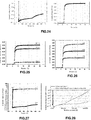
- FIG. 24 The figure 24 shows the characteristic of an electron gas transistor in a left off state and the characteristic of the same electron gas transistor in a right on state.
- the current passing through the transistor is very low compared to the current passing through the transistor in the on state, of the order of 10 to 10 times lower, for higher voltages, of the order ten times higher.
- the transistor therefore has a very high resistance blocking the current and in the on state, a low resistance allowing the conduction of the current.
- a second aspect of the invention relates to a one-piece device comprising at least two cascode transistors, that is to say two transistors in series through which the same current passes.
- FIG. 11 shows a schematic representation of a first embodiment of the device 100 according to the invention.
- FIG. 14 shows a schematic representation of a second embodiment of the device 200 according to the invention.
- FIG. 16 shows a schematic representation of a third embodiment of the device 300 according to the invention.
- FIG. 19 shows a schematic representation of a fourth embodiment of the device 400 according to the invention.
- the device 100, 200, 300, 400 comprises at least two transistors TR symmetrical with respect to a plane perpendicular to a layer plane P and comprising a vertical axis Y.
- the plane of layer P has a horizontal X axis and is perpendicular to the vertical Y axis.
- figures 29 to 34 and 37 to 40 only represent a transistor TR of the device, the complete device being obtainable by axial symmetry.
- the term “thickness of a layer” is understood to mean the dimension of the layer in the vertical direction Y perpendicular to the layer plane P.
- the electron gas characteristic of electron gas transistors is formed at the interface between the first semiconductor layer 101 and the second semiconductor layer 102.
- the first semiconductor layer 101 is for example made of gallium nitride GaN and the second semiconductor layer 102 of gallium aluminum nitride AIGaN.
- the level of aluminum in the second semiconductor layer 102 is for example greater than 20%.
- the first semiconductor layer 101 has for example a thickness between 50 nm and 300 nm and the second semiconductor layer 102 has for example a thickness greater than 20 nm.
- the third semiconductor layer 103 has P-type doping.
- the third semiconductor layer 103 is for example gallium nitride GaN doped with magnesium Mg with a dopant concentration of the order of 10 17 or 10 18 cm -3 .
- the third semiconductor layer 103 is for example gallium aluminum nitride AIGaN with an aluminum gradient along the vertical axis Y perpendicular to the plane of the P layers, doped with magnesium Mg with a dopant concentration of the order of 10 17 or 10 18 cm -3 .
- the mole fraction of aluminum for the lower part of the third semiconductor layer 103 in contact with the second semiconductor layer 102, or first mole fraction of aluminum, is less than the mole fraction of aluminum for the upper part of the third layer semiconductor 103, or second aluminum mole fraction.
- the first molar fraction of aluminum is for example of the order of the molar fraction of aluminum of the second semiconductor layer 102.
- the first molar fraction of aluminum is preferably equal to the molar fraction of aluminum of the second. semiconductor layer 102.
- the second molar fraction of aluminum is, for example, zero.
- the third semiconductor layer 103 is then produced by known techniques, for example by growth by epitaxy.
- the third semiconductor layer 103 has for example a thickness between 25 and 100 nm, more particularly between 50 and 100 nm.
- Each first zone 107, 107 ' has at least one part formed in the thickness of the third semiconductor layer 103, in other words a part of the third semiconductor layer 103 has an N-type doping.
- Each first zone 107, 107 ′ is for example doped with silicon Si or germanium Ge, for example with a dopant concentration of the order of 10 19 cm -3 to 10 20 cm -3 .
- the first zone 107, 107 ′ has for example a thickness of 20 nm to 70 nm.
- each transistor TR of the device 100, 300 comprises a single first zone 107, 107 'delimiting the source zone 107' and in the second and the fourth embodiment, each transistor TR of the device 200, 400 comprises two first zones 107, 107 ′, one of which delimits the source zone 107 ′.
- the source electrode S is formed on the source area 107 '.
- the drain electrode D is formed on or in the first semiconductor layer 101.
- the gate G is formed on a part of the third semiconductor layer 103 not doped N, that is to say not forming part of a first zone 107.
- Each transistor TR can also include a fourth semiconductor layer 104 formed on the third semiconductor layer 103 and arranged according to the layer plane P.
- the fourth semiconductor layer 104 is for example made of intrinsic gallium nitride GaN.
- the fourth semiconductor layer 104 can also be doped, with a dopant concentration of the order of 10 14 or 10 15 cm -3 .
- the transistor TR comprises a single second zone 108 with N-type doping with a dopant concentration greater than that of the first zone 107.
- the second zone 108 is for example doped with silicon Si, for example with a concentration of the order of 10 20 cm -3 .
- the second zone 108 has at least one part formed in the thickness of the third semiconductor layer 103, of the second semiconductor layer 102 and in a part of the thickness of the first semiconductor layer 101, that is to say that at the level of the second zone 108, the whole of the third semiconductor layer 103, the whole of the second semiconductor layer 102 and a part of the first semiconductor layer 101 are N doped.
- the transistor TR according to the first embodiment comprises the fourth semiconductor layer 104
- the second zone 108 is formed in the thickness of the fourth semiconductor layer 104, that is to say that at the level of the second zone 108, the entire fourth semiconductor layer 104 is N-doped.
- the device 100 according to a first embodiment and the device 300 according to a third embodiment comprise transistors TR according to the first embodiment.
- the transistor TR comprises at least one second metallic zone 201, 401, 402.
- the device 200 according to a second embodiment and the device 400 according to a fourth embodiment comprise transistors TR according to the second embodiment.
- each transistor TR comprises a single second zone 201.
- the second zone 201 is formed in the thickness of the third semiconductor layer 103, of the second semiconductor layer 102 and in part of the thickness of the first semiconductor layer 101, that is to say at the level of the second zone 201, the whole of the third semiconductor layer 103, the whole of the second semiconductor layer 102 and a part of the first semiconductor layer 101 have a metallic part.
- the transistor TR comprises the fourth semiconductor layer 104
- the second zone 201 is formed in the thickness of the fourth semiconductor layer 104, that is to say that at the level of the second zone 201, the entire fourth semiconductor layer 104 has a metal part.
- each transistor TR comprises two second zones 401, 402.
- a first second zone 401 is formed in the thickness of the second semiconductor layer 102 and in a part of the thickness of the first semiconductor layer 101, that is to say that at the level of the second zone 401, the whole of the second semiconductor layer 102 and a part of the first semiconductor layer 101 have a metallic part, and a second second zone 402 present at the at least one part in contact with a first zone 107, 107 'located between the source S and the first second zone 401.
- the gate G is located between the source electrode S and the second zone 108, 201, 401, 402.
- a third aspect of the invention relates to a method of manufacturing a device 100, 200, 300, 400 according to the invention.
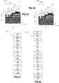
- FIG. 20 is a block diagram illustrating the steps of a first embodiment of the method 500 according to the invention, making it possible to manufacture the device 100 according to the first embodiment.
- FIG. 21 is a block diagram illustrating the steps of a second embodiment of the method 600 according to the invention, making it possible to manufacture the device 200 according to the second embodiment.
- FIG. 22 is a block diagram illustrating the steps of a third embodiment of the method 700 according to the invention, making it possible to manufacture the device 300 according to the third embodiment.
- FIG. 23 is a block diagram illustrating the steps of a fourth embodiment of the method 800 according to the invention, making it possible to manufacture the device 400 according to the fourth embodiment.
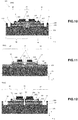
- FIG. 1 The figure 1 illustrates a first step 501 of the first embodiment of the method 500 according to the invention regardless of the embodiment.
- the first step 501 consists of depositing on a substrate not shown, along the layer plane P, the first semiconductor layer 101, the second semiconductor layer 102, the third semiconductor layer 103, optionally of the fourth semiconductor layer 104, of an insulating gate layer 105 and of a metallic gate layer 106 in that order.
- the device 100, 200, 300, 400 is shown with the optional fourth semiconductor layer 104.
- the deposition is for example carried out by epitaxy, by CVD for “Chemical Vapor Deposition” or alternatively by ALD for “Atomic Layer Deposition”.
- the insulating gate layer 105 has for example a thickness comprised between 10 nm and 80 nm and the metallic gate layer 106 has for example a thickness comprised between 10 nm and 200 nm.
- the insulating gate layer 105 is for example made of silicon nitride SiN or of Al 2 O 3 or of HfO 2 and the metallic gate layer 106 is for example of TiN or of p-type doped poly-Si Al.
- FIG. 2 The figure 2 illustrates a second step 502 of the method 500, 600, 700, 800 according to the invention regardless of the embodiment.
- the second step 502 consists in etching the insulating gate layer 105 and the metallic gate layer 106 with stopping on the fourth semiconductor layer 104, or failing this with stopping on the third semiconductor layer 103, so as to obtain two first parallel lines L1. and not confused in the P layer plane.
- the etching is for example carried out by fluorinated dry plasma etching.
- the first lines L1 are for example spaced from one another by 50 nm to 0.5 ⁇ m and have a width of 100 nm to 1 ⁇ m.
- FIG. 3 The figure 3 illustrates a third step 503 of the method 500, 600, 700, 800 according to the invention regardless of the embodiment.
- the third step 503 consists in doping the peripheral zones ZP located on either side of the first two lines L1 comprising the parts of the fourth semiconductor layer 104, or failing that of the third semiconductor layer 103, exposed in the second step 502.
- Doping is for example carried out by ion implantation of a dose of 2 ⁇ 10 15 cm 2 at 40 keV. It is then followed by annealing of temperature 1000 ° C or above for about 30 min.
- the third step 503 allows the creation of the first zones 107.
- the third step 503 allows the creation of the second N-type doped zones 108.
- the characteristics of the doping of the third step 503 are therefore different depending on the embodiment of the method 500, 600, 700, 800.
- the implanted dose will be greater than the dose implanted in the cells.
- the doping carried out allows the creation of the first zones 107.
- FIG. 4 The figure 4 illustrates a fourth step 504 of the method 500, 600, 700, 800 according to the invention regardless of the embodiment.
- the fourth step 504 consists in doping a central zone ZC situated between the two first lines L1 comprising the parts of the fourth semiconductor layer 104 exposed in the second step 502.
- Doping is for example carried out by ion implantation. It is then followed by annealing.
- the fourth step 504 allows the creation of the first zones 107.
- the fourth step 504 allows the creation of a second zone 108 with N-type doping.
- the characteristics of the doping of the fourth step 504 are therefore different according to the embodiment of the method 500, 600, 700, 800 according to the invention.
- the implanted dose will be greater than the implanted dose in the second, third and fourth embodiments.
- the doping carried out allows the creation of a second zone 108 with N-type doping.
- FIG. 5 The figure 5 illustrates a fifth step 505 of the method 500, 600, 700, 800 according to the invention regardless of the embodiment.
- the fifth step 505 consists in etching the parts of the fourth semiconductor layer 104, and / or, failing that, of the third semiconductor layer 103, doped during the third step 503, that is to say the peripheral zones ZP, with stop on the second semiconductor layer 102, so as to keep two second lines L2 along the two first lines L1.
- the second lines L2 are therefore mutually parallel and parallel to the first lines L1 in the P layer plane.
- the etching is for example carried out by dry etching in fluorinated plasma.
- the second lines L2 are for example spaced 250 nm to 3 ⁇ m apart and have a width of 1 ⁇ m to 10 ⁇ m.
- FIG. 6 The figure 6 illustrates a sixth step 506 of the method 500, 700, 800 according to the first, third and fourth embodiments.
- the sixth step 506 consists in depositing an insulating electrode layer 109 along the layer plane P.
- the insulating electrode layer 109 is for example made of silicon nitride SiN and for example has a thickness of 30 nm.
- the insulating electrode layer 109 is for example obtained by LPCVD deposition of a strain of SiN.
- the sixth step 506 is also carried out in the method 600 according to the second embodiment, but this is preceded by a step 601 illustrated on the figure. figure 11 .
- Step 601 illustrated in figure 11 consists in etching a primary trench T1 'with a stop on the second semiconductor layer 102, in the parts exposed in the second step 502 and located between the two first lines L1, that is to say in the central zone ZC.
- the primary trench T1 ' is parallel to the first lines L1 in the P layer plane.
- the primary trench T1 ' is etched so that the edges of this primary trench T1' are substantially of the same height and that the sides of the primary trench T1 'are included in planes orthogonal to the bottom of the primary trench T1' and substantially parallel between them.
- the etching according to a photo-lithography step can be carried out by the dry process in fluorinated plasma.
- the primary trench T1 ′ has for example a width of 0.5 ⁇ m to 9 ⁇ m.
- FIG. 7 The figure 7 illustrates a seventh step 507 of the method 500 according to the first embodiment.
- the seventh step 507 consists in etching two first trenches T1, a first trench T1 in each second line L2, with stopping on the fourth semiconductor layer 104, or failing this with stopping on the third semiconductor layer 103.
- the first trenches T1 are parallel to the first L1 lines in the P layer plane.
- the first T1 trenches are parallel to each other.
- a first trench T1 is etched so that the edges of this first trench T1 are substantially of the same height and that the sides of the first trench T1 are included in planes orthogonal to the bottom of the first trench T1 and substantially parallel to each other.
- the etching depth is substantially the same for the first two trenches T1.
- the etching according to a photo-lithography step can be carried out by the dry process in fluorinated plasma.
- the first two trenches T1 have for example a width of 0.5 ⁇ m to 10 ⁇ m.
- the seventh step 507 is also carried out in the method 600 according to the second embodiment after the sixth step 506.
- the seventh step 507 is not performed in the method 700, 800 according to the third and fourth embodiments.
- a seventh bis step is performed in its place.
- FIG. 15 The figure 15 illustrates the seventh step bis 701 of the method 700, 800 according to the third and fourth embodiments.
- the seventh bis step 701 consists in etching a first trench T1 in the parts of the fourth semiconductor layer 104, or failing that of the third semiconductor layer 103, exposed in the second step 502 located between the first two lines L1, that is to say in the central zone ZC.
- the first trench T1 is parallel to the first lines L1 in the P layer plane.
- the first trench T1 is etched so that the edges of this first trench T1 are substantially of the same height and that the sides of the first trench T1 are included in planes orthogonal to the bottom of the first trench T1 and substantially parallel to each other.
- the etching according to a photo-lithography step can be carried out by the dry process in fluorinated plasma.
- the first trench T1 has for example a width of 0.5 ⁇ m to 10 ⁇ m.
- FIG. 8 The figure 8 illustrates an eighth step 508 of the method 500 according to the first embodiment.
- the eighth step 508 consists in etching two second parallel trenches T2 with stopping on the first semiconductor layer 101 in the parts of the peripheral zones ZP situated on either side of the two second lines L2, the two second trenches T2 being separated by the two second lines L2.
- the second T2 trenches are parallel to the first lines L1 in the P layer plane.
- the second T2 trenches are mutually parallel.
- a second trench T2 is etched so that the edges of this second trench T2 are substantially of the same height and that the sides of the second trench T2 are included in planes orthogonal to the bottom of the second trench T2 and substantially parallel to each other.
- the etching depth is substantially the same for the two second trenches T2.
- the etching according to a photo-lithography step can be carried out by the dry process in fluorinated plasma.
- the two second trenches T2 have for example a width of 0.5 ⁇ m to 10 ⁇ m.
- the eighth step 508 is also carried out in the method 600 according to the second embodiment after the seventh step 507 and in the method 700 according to the third embodiment after the seventh bis step 701.
- the eighth step 508 is also carried out in the method 800 according to the fourth embodiment, after a step 801 illustrated on the figure. figure 17 and a step 802 illustrated in figure 18 .
- Step 801 illustrated in figure 17 consists in etching two primary trenches T1 'in the insulating electrode layer 109 and in a part of the fourth semiconductor layer 104, or failing the third semiconductor layer 103 doped during the third step 503, at the level of the second lines L2 .
- the primary trenches T1 ' are parallel to the first lines L1 in the P layer plane.
- the primary trenches T1 ' are mutually parallel.
- a primary trench T1 ' is etched so that the edges of this primary trench T1' are substantially of the same height and that the sides of the primary trench T1 'are included in planes orthogonal to the bottom of the primary trench T1' and substantially parallel between them.
- the etching depth is substantially the same for the two primary trenches T1 ′.
- the etching according to a photo-lithography step can be carried out by dry process in fluorinated plasma.
- the two primary trenches T1 ′ have for example a width of 0.5 ⁇ m to 10 ⁇ m.
- Step 802 illustrated in figure 18 consists in etching two secondary trenches T2 ′ with stopping on the first semiconductor layer 101 along the two second lines L2, that is to say in the peripheral zones ZP.
- the Secondary trenches T2 ' are parallel to the first lines L1 in the P layer plane.
- the secondary trenches T2 ' are parallel to each other.
- a secondary trench T2 ' is etched so that the edges of this secondary trench T2' are substantially of the same height and that the sides of the secondary trench T2 'are included in planes orthogonal to the bottom of the secondary T2' and substantially parallel between them.
- the etching depth is substantially the same for the two secondary trenches T2 ′.
- the etching according to a photo-lithography step can be carried out by the dry process in fluorinated plasma.
- the two secondary trenches T2 ′ have for example a width of 0.5 ⁇ m to 10 ⁇ m.
- FIG. 9 The figure 9 illustrates a ninth step 509 of the method 500 according to the first embodiment.
- the ninth step 509 consists in carrying out a conformal deposition of a metallic electrode layer 110.
- the deposition is for example carried out by epitaxy, by CVD for “Chemical Vapor Deposition” or alternatively by ALD for “Atomic Layer Deposition”.
- the metallic electrode layer 110 is for example made of TiN or of Ti and has a thickness of between 50 nm and 100 nm.
- the ninth step 509 is also performed in the method 700 according to the third embodiment and in the method 800 according to the fourth embodiment after the eighth step 508.
- the ninth step 509 is also carried out in the method 600 according to the second embodiment, after a step 602 illustrated on the figure. figure 12 and a step 603 illustrated in figure 13 .
- Step 602 illustrated in figure 12 consists in etching a secondary trench T2 'in the primary trench engraved in step 601 illustrated on figure 11 with stop in the first semiconductor layer 101.
- the secondary trench T2 ′ is parallel to the first lines L1 in the layer plane P.
- a secondary trench T2 ' is etched so that the edges of this secondary trench T2' are substantially of the same height and that the sides of the secondary trench T2 'are included in planes orthogonal to the bottom of the secondary T2' and substantially parallel between them.
- the etching according to a photo-lithography step can be carried out by dry process in fluorinated plasma.
- the secondary trench T2 ′ has for example a width of 0.5 ⁇ m to 10 ⁇ m.
- Step 603 illustrated in figure 13 consists in etching at least two tertiary trenches T3 'in the central zone on either side of the primary trench T1' engraved in step 601.
- the tertiary trenches T3 ' are parallel to the first lines L1 in the layer plane P .
- a tertiary trench T3 ' is engraved so that the edges of this tertiary trench T3' are substantially of the same height and that the sides of the tertiary trench T3 'are included in planes orthogonal to the bottom of the tertiary T3' and substantially parallel between them.
- the etching according to a photo-lithography step can be carried out by dry process in fluorinated plasma.
- the tertiary trenches T3 ′ have for example a width of 0.5 ⁇ m to 10 ⁇ m.
- FIG. 10 The figure 10 illustrates a tenth step 510 of the method 500 according to the first embodiment.
- the tenth step 510 consists in etching the metallic electrode layer 110 so as to keep the metallic electrode layer 110 at the level of the previously etched trenches T1, T2, T1 ', T2'.
- the tenth step 510 is also carried out in the method 600, 700, 800 according to the second, third and fourth embodiments after the ninth step 509.
- the parts of the metallic electrode layer 110 located in the first trenches T1 become the source electrodes S
- the parts of the metallic electrode layer 110 located in the second trenches T2 become the drain electrodes D
- the conduction path is not rectilinear and the electrons coming from the source electrode S pass through the second semiconductor layer 102 via a second zone 108, 201, 401 to reach the drain electrode D.
- FIG. 25 The figure 25 represents the characteristics of a transistor TR according to the invention in its on state as a function of the thickness of the second semiconductor layer 102.
- FIG. 26 The figure 26 represents the characteristics of a transistor TR according to the invention in its on state as a function of the percentage of aluminum Al in the second semiconductor layer 102 made of aluminum-gallium nitride.
- FIG. 27 The figure 27 represents the characteristics of a transistor TR according to the invention in its off state as a function of the dopant concentration in the third semiconductor layer 103.
- the resistance of the transistor TR in the on state can therefore be adjusted via the characteristics of the second semiconductor layer 102 and the resistance in the off state and therefore the threshold voltage, via the characteristics of the third. semiconductor layer 103.
- the resistance of transistor TR in its on state is decorrelated from its threshold voltage, unlike conventional electron gas transistors in which the characteristics of the second semiconductor layer 102 also impact the resistance in the off state.
- FIG. 28 The figure 28 shows in black dotted lines the leakage current of a transistor TR according to the invention having a third semiconductor layer of P-doped GaN gallium nitride and in red dotted lines the leakage current of a transistor TR according to the invention having a third layer P-doped GaN aluminum-gallium nitride semiconductor with an aluminum gradient along the vertical Y axis having a first aluminum mole fraction equal to 0.2 and a second zero aluminum mole fraction.
- the third semiconductor layer is doped with magnesium Mg with a dopant concentration of the order of 5 x10 18 cm -3 .
- the leakage current in the transistor TR having a third semiconductor layer made of GaN aluminum-gallium nitride P doped with a vertical aluminum gradient is less than the leakage current in the transistor TR according to the invention having a third P-doped GaN gallium nitride semiconductor layer.
- the monobloc device according to the second aspect of the invention may further include a Schottky diode integrated in parallel with each transistor TR.
- FIG. 31 shows a schematic representation of a first variant embodiment of a transistor TR of a fifth embodiment of the device 1100 according to the invention, incorporating a Schottky diode.
- FIG. 34 shows a schematic representation of a first variant embodiment of a transistor TR of a sixth embodiment of the device 1200 according to the invention, incorporating a Schottky diode.
- FIG. 38 shows a schematic representation of a transistor TR of a seventh embodiment of the device 1300 according to the invention, incorporating a Schottky diode.
- FIG. 40 shows a schematic representation of a transistor TR of an eighth embodiment of the device 1400 according to the invention, incorporating a Schottky diode.
- FIG. 35 is a block diagram illustrating the steps of a first variant embodiment of the fifth embodiment of the method 900 according to the invention making it possible to obtain the first variant embodiment of the fifth embodiment of the device 1100 according to the invention.
- the fifth embodiment of the method 900 according to the invention further comprises three steps with respect to the first embodiment 500, or to the second embodiment 600 of the method according to the invention.
- the first variant embodiment of the fifth embodiment of the device 1100 according to the invention makes it possible to obtain the fifth embodiment of the device 1100 according to the invention from the first embodiment of the device 100 according to the invention.
- the same lessons can be applied to obtain a second variant embodiment of the fifth embodiment of the device 1100 according to the invention from the second embodiment of the device 200 according to the invention.
- the fifth embodiment of the method 900 according to the invention comprises the first eight steps 501, 502, 503, 504, 505, 506, 507, 508 of the first embodiment of the method 500 according to the invention.
- FIG. 29 illustrates a ninth step 901 of the first variant embodiment of the fifth embodiment of the method 900 according to the invention.
- the ninth step 901 could be carried out before the steps 507 and 508 of etching the first trenches T1 and the second trenches T2.
- the ninth step 901 consists in etching two third parallel trenches T3 in the insulating electrode layer 109, at the level of the peripheral zones ZP situated on either side of the two second lines L2 so that the second lines L2 are between the two. third trenches T3.
- Each third trench T3 is between a first trench T1 and a second trench T2.
- the third trenches T3 are parallel to the first trenches T1 and to the second trenches T2.
- the etching according to a photo-lithography step can be carried out by the dry process in fluorinated plasma.
- the ninth step 901 is followed by the ninth step 509 and the tenth step 510 of the first embodiment of the method 500 according to the invention, corresponding respectively to the tenth and eleventh step of the first variant embodiment of the fifth embodiment of the method 900 according to the invention, the electrode etching carried out during the tenth step 510 further preserving the metallic electrode layer 110 between each third trench T3 etched in the ninth step 901 and the first trench T1 closest to the third T3 trench considered.
- the tenth step 510 of the first embodiment of the method 500 according to the invention is followed by a twelfth step and a thirteenth step in the method 900.
- FIG. 30 The figure 30 illustrates the twelfth step 902 of the first variant embodiment of the fifth embodiment of the method 900 according to the invention.
- FIG. 31 The figure 31 illustrates the thirteenth step 903 of the first variant embodiment of the fifth embodiment of the method 900 according to the invention.
- the twelfth step 902 consists in depositing a metallic diode layer 111 according to the layer plane P.
- the deposition is for example carried out by CVD for “Chemical Vapor Deposition” or by spraying or sputtering in English.
- the metallic diode layer 111 is for example made of Ni or Ni-Au and has a thickness of between 10 nm and 500 nm.
- the thirteenth step 903 consists in etching the metallic diode layer 111 so as to keep at least the metallic diode layer 111 at the level of each third trench T3 etched in the ninth step 901 and between each third trench T3 and the first trench T1 closest to the third trench T3 considered.
- the remaining metallic diode layer 111 constitutes a Schottky Sc diode.
- the first variant embodiment of the fifth embodiment of the device 1100 according to the invention is obtained.
- FIG. 36 is a block diagram illustrating the steps of a first variant embodiment of the sixth embodiment of the method 1000 according to the invention making it possible to obtain the first variant embodiment of the sixth embodiment of the device 1200 according to the invention.
- the sixth embodiment of the method 1000 according to the invention further comprises two steps with respect to the first embodiment 500, or to the second embodiment 600 of the method according to the invention.
- the first variant embodiment of the sixth embodiment of the device 1200 according to the invention makes it possible to obtain the sixth embodiment of the device 1200 according to the invention from the first embodiment of the device 100 according to the invention.
- the same lessons can be applied to obtain a second variant embodiment of the sixth embodiment of the device 1100 according to the invention from the second embodiment of the device 200 according to the invention.
- the sixth embodiment of the method 1000 according to the invention comprises the first six steps 501, 502, 503, 504, 505, 506, of the first embodiment of the method 500 according to the invention.
- FIG. 32 The figure 32 illustrates a seventh step 1001 of the first variant embodiment of the sixth embodiment of the method 1000 according to the invention.
- the seventh step 1001 consists in etching two third parallel trenches T3 in the insulating electrode layer 109, at the level of the peripheral zones. ZP located on either side of the two second lines L2 so that the second lines L2 are between the two third trenches T3.
- the etching according to a photo-lithography step can be carried out by the dry process in fluorinated plasma.
- the seventh step 1001 then consists in depositing a metallic diode layer 111 according to the layer plane P.
- the deposition is for example carried out by CVD for “Chemical Vapor Deposition” or by spraying or sputtering in English.
- the metallic diode layer 111 is for example made of Ni or Ni-Au and has a thickness of between 10 nm and 500 nm.
- FIG. 33 The figure 32 illustrates the eighth step 1002 of the first variant embodiment of the sixth embodiment of the method 1000 according to the invention.
- the eighth step 1002 consists in etching the metallic diode layer 111 so as to keep at least the metallic diode layer 111 at the level of each third trench T3, between each third trench T3 and the second line L2 closest to the third trench T3 considered and at the level of each second line L2.
- the eighth step 1002 then consists in depositing an insulating diode layer 112 along the layer plane P.
- the insulating diode electrode layer 112 is for example made of silicon nitride SiN and for example has a thickness of between 10 and 500 nm.
- the insulating diode electrode layer 112 is for example obtained by LPCVD deposition of a strain of SiN.
- the eighth step 1002 is followed by the seventh step 507, the eighth step 508, the ninth step 509 and the tenth step 510 of the first embodiment of the method 500 according to the invention, corresponding respectively to the ninth, tenth, eleventh. and twelfth step of the first variant embodiment of the sixth embodiment of the method 1000 according to the invention, the second trenches T2 being etched so that the third trenches T3 are between the second trenches T2 and the electrode etching carried out during the tenth step 510 further retaining the metallic electrode layer 110 in each third trench T3 and between each third trench T3 and the first trench T1 closest to the third trench T3 considered.
- each third trench T3 is between a first trench T1 and a second trench T2 and the third trenches T3 are parallel to the first trenches T1 and to the second trenches T2.
- the first variant embodiment of the sixth embodiment of the device 1200 according to the invention illustrated in figure 34 is obtained, the remaining metallic diode layer 111 covered with the metallic electrode layer 110 constituting a Schottky diode Sc.
- FIG. 41 is a block diagram illustrating the steps of the seventh embodiment of the method 1500 according to the invention making it possible to obtain the seventh embodiment of the device 1300 according to the invention.
- the seventh embodiment of the method 1500 according to the invention further comprises two steps with respect to the third embodiment 700 of the method according to the invention.
- the seventh embodiment of the device 1300 according to the invention makes it possible to obtain the seventh embodiment of the device 1300 according to the invention from the third embodiment of the device 300 according to the invention.
- the seventh embodiment of the method 1500 according to the invention comprises the ten steps 501, 502, 503, 504, 505, 506, 701, 508, 509, 510 of the third embodiment of the method 700 according to the invention.
- FIG. 37 The figure 37 illustrates the eleventh step 1501 of the seventh embodiment of the method 1500 according to the invention.
- the eleventh step 1501 consists in etching two third parallel trenches T3 so that each third trench is etched at the level of a second line L2.
- Each third trench T3 is between the first trench T1 and a second trench T2 and the third trenches T3 are parallel to the first trench T1 and to the second trenches T2.
- the etching according to a photo-lithography step can be carried out by the dry process in fluorinated plasma.
- FIG. 38 The figure 38 illustrates the twelfth step 1502 of the seventh embodiment of the method 1500 according to the invention.
- the twelfth step 1502 consists in depositing a metallic diode layer 111 according to the layer plane P.
- the deposition is for example carried out by CVD for “Chemical Vapor Deposition” or by spraying or sputtering in English.
- the metallic diode layer 111 is for example made of Ni or Ni-Au and has a thickness of between 10 nm and 500 nm.
- the twelfth step 1502 then consists in etching the metallic diode layer 111 so as to keep at least the metallic diode layer 111 at the level of each second line L2, between each third trench T3 and the first trench T1 and at the level of the first T1 trench.
- the seventh embodiment of the device 1300 according to the invention illustrated in figure 38 is obtained, the remaining metallic diode layer 111 constituting a Schottky diode Sc.
- FIG. 42 is a block diagram illustrating the steps of the eighth embodiment of the method 1600 according to the invention making it possible to obtain the eighth embodiment of the device 1400 according to the invention.
- the eighth embodiment of the method 1600 according to the invention further comprises two steps with respect to the fourth embodiment of the method 800 according to the invention.
- the eighth embodiment of the device 1400 according to the invention makes it possible to obtain the eighth embodiment of the device 1400 according to the invention from the fourth embodiment of the device 400 according to the invention.
- the eighth embodiment of method 1600 according to the invention comprises the twelve steps 501, 502, 503, 504, 505, 506, 701, 801, 802, 508, 509, 510 of the fourth embodiment of method 800 according to invention.
- FIG. 39 The figure 39 illustrates the thirteenth step 1601 of the eighth embodiment of the method 1600 according to the invention.
- the thirteenth step 1601 consists in depositing an insulating diode layer 112 along the layer plane P.
- the insulating diode electrode layer 112 is for example made of silicon nitride SiN and for example has a thickness of between 10 and 500 nm.
- the insulating diode electrode layer 112 is for example obtained by LPCVD deposition of a strain of SiN.
- the thirteenth step 1601 then consists in etching two third parallel trenches T3 so that each third trench is etched between a second trench T2 and a secondary trench T2 ′.
- the third trenches T3 are parallel to the first trench T1, to the primary trenches T1 ', to the secondary trenches T2' and to the second trenches T2.
- the etching according to a photo-lithography step can be carried out by the dry process in fluorinated plasma.
- FIG. 40 The figure 40 illustrates the fourteenth step 1602 of the eighth embodiment of the method 1600 according to the invention.
- the fourteenth step 1602 consists in depositing a metallic diode layer 111 according to the layer plane P.
- the deposition is for example carried out by CVD for “Chemical Vapor Deposition” or by spraying or sputtering in English.
- the metallic diode layer 111 is for example made of Ni or Ni-Au and has a thickness of between 10 nm and 500 nm.
- the fourteenth step 1602 then consists in etching the metallic diode layer 111 so as to keep at least the metallic diode layer 111 at the level of each third trench T3, between each third trench T3 and the first trench T1 and at the level of the first T1 trench.
- the eighth embodiment of the device 1400 according to the invention illustrated in figure 40 is obtained, the remaining metallic diode layer 111 constituting a Schottky diode Sc.
Landscapes
- Junction Field-Effect Transistors (AREA)
- Metal-Oxide And Bipolar Metal-Oxide Semiconductor Integrated Circuits (AREA)
- Insulated Gate Type Field-Effect Transistor (AREA)
Applications Claiming Priority (1)
| Application Number | Priority Date | Filing Date | Title |
|---|---|---|---|
| FR1912957A FR3103321B1 (fr) | 2019-11-20 | 2019-11-20 | Transistor a gaz d’electrons, dispositif monobloc comportant au moins deux transistors en cascode et procedes de fabrication associes |
Publications (1)
| Publication Number | Publication Date |
|---|---|
| EP3826072A1 true EP3826072A1 (de) | 2021-05-26 |
Family
ID=69811052
Family Applications (1)
| Application Number | Title | Priority Date | Filing Date |
|---|---|---|---|
| EP20208298.8A Pending EP3826072A1 (de) | 2019-11-20 | 2020-11-18 | Elektronengas-transistor, monoblock-vorrichtung, die mindestens zwei transistoren in kaskadenschaltung umfasst, und entsprechendes herstellungsverfahren |
Country Status (3)
| Country | Link |
|---|---|
| US (1) | US11489067B2 (de) |
| EP (1) | EP3826072A1 (de) |
| FR (1) | FR3103321B1 (de) |
Families Citing this family (2)
| Publication number | Priority date | Publication date | Assignee | Title |
|---|---|---|---|---|
| FR3103321B1 (fr) * | 2019-11-20 | 2021-12-17 | Commissariat Energie Atomique | Transistor a gaz d’electrons, dispositif monobloc comportant au moins deux transistors en cascode et procedes de fabrication associes |
| FR3105409B1 (fr) * | 2019-12-19 | 2021-12-17 | Commissariat Energie Atomique | Composant de détection de rayonnement électromagnétique à haute sensibilité et procédé de fabrication d’un tel composant |
Citations (2)
| Publication number | Priority date | Publication date | Assignee | Title |
|---|---|---|---|---|
| US20050145883A1 (en) * | 2003-12-05 | 2005-07-07 | Robert Beach | III-nitride semiconductor device with trench structure |
| US20080308908A1 (en) * | 2007-06-12 | 2008-12-18 | Rohm Co., Ltd. | Nitride semiconductor device and method for producing nitride semiconductor device |
Family Cites Families (1)
| Publication number | Priority date | Publication date | Assignee | Title |
|---|---|---|---|---|
| FR3103321B1 (fr) * | 2019-11-20 | 2021-12-17 | Commissariat Energie Atomique | Transistor a gaz d’electrons, dispositif monobloc comportant au moins deux transistors en cascode et procedes de fabrication associes |
-
2019
- 2019-11-20 FR FR1912957A patent/FR3103321B1/fr active Active
-
2020
- 2020-11-18 US US16/951,647 patent/US11489067B2/en active Active
- 2020-11-18 EP EP20208298.8A patent/EP3826072A1/de active Pending
Patent Citations (2)
| Publication number | Priority date | Publication date | Assignee | Title |
|---|---|---|---|---|
| US20050145883A1 (en) * | 2003-12-05 | 2005-07-07 | Robert Beach | III-nitride semiconductor device with trench structure |
| US20080308908A1 (en) * | 2007-06-12 | 2008-12-18 | Rohm Co., Ltd. | Nitride semiconductor device and method for producing nitride semiconductor device |
Non-Patent Citations (1)
| Title |
|---|
| E.A. JONES ET AL., IEEE JOURNAL OF EMERGING AND SELECTED TOPICS IN POWER ELECTRONICS, vol. 4, no. 3, September 2016 (2016-09-01), pages 707 - 719 |
Also Published As
| Publication number | Publication date |
|---|---|
| US20210184027A1 (en) | 2021-06-17 |
| US11489067B2 (en) | 2022-11-01 |
| FR3103321A1 (fr) | 2021-05-21 |
| FR3103321B1 (fr) | 2021-12-17 |
Similar Documents
| Publication | Publication Date | Title |
|---|---|---|
| EP0017531B1 (de) | Feldeffekttransistor mit hoher Grenzfrequenz und Verfahren zu dessen Herstellung | |
| EP2736078B1 (de) | Bidirektionaler Transistor mit hoher Elektronenbeweglichkeit | |
| EP3203526B1 (de) | Transistor mit heteroübergang mit verbessertem elektronengas-einschluss | |
| EP2736079B1 (de) | Herstellungsverfahren eines Transistors mit Heteroübergang vom Typ, der normalerweise blockiert ist | |
| EP3203527B1 (de) | Selbstsperrender transistor mit heteroübergang mit hoher elektronenbeweglichkeit | |
| FR3050869A1 (fr) | Transistor a heterojonction de type normalement ouvert a tension de seuil elevee | |
| EP3718143A1 (de) | Elektronisches bauelement mit einem heteroübergang mit einer verbesserten eingebetteten sperrschicht | |
| EP3549172A1 (de) | Heteroübergangstransistor mit vertikaler struktur | |
| EP2992558B1 (de) | Verfahren zur herstellung eines implantierten bereichs für einen normal blockierten heteroübergangstransistor | |
| EP3235006A1 (de) | Hemt-transistor | |
| EP4318597A1 (de) | Feldeffekttransistor mit p-fet-verhalten | |
| EP3369115A1 (de) | Feldeffekttransistor mit optimierter leistung und verstärkung | |
| EP2685504A1 (de) | Tunneleffekttransistor | |
| EP3561880A1 (de) | Hemt und herstellungsverfahren welches eine geringere gatelänge und einen geringeren gate-leckverlust begünstigt | |
| EP3826072A1 (de) | Elektronengas-transistor, monoblock-vorrichtung, die mindestens zwei transistoren in kaskadenschaltung umfasst, und entsprechendes herstellungsverfahren | |
| EP0051504A1 (de) | Feldeffekttransistor mit einem kurzen Kanal | |
| FR2496990A1 (fr) | Transistor a effet de champ a barriere schottky | |
| EP1517377A1 (de) | Bipolartransistor | |
| WO2019224448A1 (fr) | Transistor a haute mobilite electronique en mode enrichissement | |
| FR3053832A1 (fr) | Procede de fabrication d'un transistor a heterojonction a effet de champ et transistor correspondant | |
| EP3591709A1 (de) | Selbstsperrender transistor mit heteroübergang und vermindertem durchgangswiderstand | |
| FR2550888A1 (fr) | Transistor a effet de champ a grille ultracourte et a structure horizontale, et son procede de fabrication | |
| EP3624202A1 (de) | Bidirektionaler transistor mit heterostruktur und geringem durchlasswiderstand |
Legal Events
| Date | Code | Title | Description |
|---|---|---|---|
| PUAI | Public reference made under article 153(3) epc to a published international application that has entered the european phase |
Free format text: ORIGINAL CODE: 0009012 |
|
| STAA | Information on the status of an ep patent application or granted ep patent |
Free format text: STATUS: REQUEST FOR EXAMINATION WAS MADE |
|
| 17P | Request for examination filed |
Effective date: 20201118 |
|
| AK | Designated contracting states |
Kind code of ref document: A1 Designated state(s): AL AT BE BG CH CY CZ DE DK EE ES FI FR GB GR HR HU IE IS IT LI LT LU LV MC MK MT NL NO PL PT RO RS SE SI SK SM TR |
|
| RBV | Designated contracting states (corrected) |
Designated state(s): AL AT BE BG CH CY CZ DE DK EE ES FI FR GB GR HR HU IE IS IT LI LT LU LV MC MK MT NL NO PL PT RO RS SE SI SK SM TR |
|
| RAP3 | Party data changed (applicant data changed or rights of an application transferred) |
Owner name: COMMISSARIAT A L'ENERGIE ATOMIQUE ET AUX ENERGIESALTERNATIVES |