EP3848961B1 - Dispositif à semi-conducteur - Google Patents
Dispositif à semi-conducteur Download PDFInfo
- Publication number
- EP3848961B1 EP3848961B1 EP18932539.2A EP18932539A EP3848961B1 EP 3848961 B1 EP3848961 B1 EP 3848961B1 EP 18932539 A EP18932539 A EP 18932539A EP 3848961 B1 EP3848961 B1 EP 3848961B1
- Authority
- EP
- European Patent Office
- Prior art keywords
- scale
- resin
- semiconductor device
- lead frame
- heat dissipation
- Prior art date
- Legal status (The legal status is an assumption and is not a legal conclusion. Google has not performed a legal analysis and makes no representation as to the accuracy of the status listed.)
- Active
Links
Images



Classifications
-
- H—ELECTRICITY
- H10—SEMICONDUCTOR DEVICES; ELECTRIC SOLID-STATE DEVICES NOT OTHERWISE PROVIDED FOR
- H10W—GENERIC PACKAGES, INTERCONNECTIONS, CONNECTORS OR OTHER CONSTRUCTIONAL DETAILS OF DEVICES COVERED BY CLASS H10
- H10W74/00—Encapsulations, e.g. protective coatings
- H10W74/10—Encapsulations, e.g. protective coatings characterised by their shape or disposition
-
- H—ELECTRICITY
- H10—SEMICONDUCTOR DEVICES; ELECTRIC SOLID-STATE DEVICES NOT OTHERWISE PROVIDED FOR
- H10W—GENERIC PACKAGES, INTERCONNECTIONS, CONNECTORS OR OTHER CONSTRUCTIONAL DETAILS OF DEVICES COVERED BY CLASS H10
- H10W70/00—Package substrates; Interposers; Redistribution layers [RDL]
- H10W70/40—Leadframes
- H10W70/421—Shapes or dispositions
- H10W70/424—Cross-sectional shapes
-
- H—ELECTRICITY
- H10—SEMICONDUCTOR DEVICES; ELECTRIC SOLID-STATE DEVICES NOT OTHERWISE PROVIDED FOR
- H10W—GENERIC PACKAGES, INTERCONNECTIONS, CONNECTORS OR OTHER CONSTRUCTIONAL DETAILS OF DEVICES COVERED BY CLASS H10
- H10W40/00—Arrangements for thermal protection or thermal control
- H10W40/20—Arrangements for cooling
- H10W40/22—Arrangements for cooling characterised by their shape, e.g. having conical or cylindrical projections
- H10W40/226—Arrangements for cooling characterised by their shape, e.g. having conical or cylindrical projections characterised by projecting parts, e.g. fins to increase surface area
- H10W40/228—Arrangements for cooling characterised by their shape, e.g. having conical or cylindrical projections characterised by projecting parts, e.g. fins to increase surface area the projecting parts being wire-shaped or pin-shaped
-
- H—ELECTRICITY
- H10—SEMICONDUCTOR DEVICES; ELECTRIC SOLID-STATE DEVICES NOT OTHERWISE PROVIDED FOR
- H10W—GENERIC PACKAGES, INTERCONNECTIONS, CONNECTORS OR OTHER CONSTRUCTIONAL DETAILS OF DEVICES COVERED BY CLASS H10
- H10W70/00—Package substrates; Interposers; Redistribution layers [RDL]
- H10W70/01—Manufacture or treatment
- H10W70/04—Manufacture or treatment of leadframes
-
- H—ELECTRICITY
- H10—SEMICONDUCTOR DEVICES; ELECTRIC SOLID-STATE DEVICES NOT OTHERWISE PROVIDED FOR
- H10W—GENERIC PACKAGES, INTERCONNECTIONS, CONNECTORS OR OTHER CONSTRUCTIONAL DETAILS OF DEVICES COVERED BY CLASS H10
- H10W70/00—Package substrates; Interposers; Redistribution layers [RDL]
- H10W70/40—Leadframes
- H10W70/461—Leadframes specially adapted for cooling
-
- H—ELECTRICITY
- H10—SEMICONDUCTOR DEVICES; ELECTRIC SOLID-STATE DEVICES NOT OTHERWISE PROVIDED FOR
- H10W—GENERIC PACKAGES, INTERCONNECTIONS, CONNECTORS OR OTHER CONSTRUCTIONAL DETAILS OF DEVICES COVERED BY CLASS H10
- H10W74/00—Encapsulations, e.g. protective coatings
- H10W74/01—Manufacture or treatment
- H10W74/016—Manufacture or treatment using moulds
-
- H—ELECTRICITY
- H10—SEMICONDUCTOR DEVICES; ELECTRIC SOLID-STATE DEVICES NOT OTHERWISE PROVIDED FOR
- H10W—GENERIC PACKAGES, INTERCONNECTIONS, CONNECTORS OR OTHER CONSTRUCTIONAL DETAILS OF DEVICES COVERED BY CLASS H10
- H10W74/00—Encapsulations, e.g. protective coatings
- H10W74/10—Encapsulations, e.g. protective coatings characterised by their shape or disposition
- H10W74/111—Encapsulations, e.g. protective coatings characterised by their shape or disposition the semiconductor body being completely enclosed
-
- H—ELECTRICITY
- H10—SEMICONDUCTOR DEVICES; ELECTRIC SOLID-STATE DEVICES NOT OTHERWISE PROVIDED FOR
- H10W—GENERIC PACKAGES, INTERCONNECTIONS, CONNECTORS OR OTHER CONSTRUCTIONAL DETAILS OF DEVICES COVERED BY CLASS H10
- H10W74/00—Encapsulations, e.g. protective coatings
- H10W74/10—Encapsulations, e.g. protective coatings characterised by their shape or disposition
- H10W74/111—Encapsulations, e.g. protective coatings characterised by their shape or disposition the semiconductor body being completely enclosed
- H10W74/127—Encapsulations, e.g. protective coatings characterised by their shape or disposition the semiconductor body being completely enclosed characterised by arrangements for sealing or adhesion
-
- H—ELECTRICITY
- H10—SEMICONDUCTOR DEVICES; ELECTRIC SOLID-STATE DEVICES NOT OTHERWISE PROVIDED FOR
- H10W—GENERIC PACKAGES, INTERCONNECTIONS, CONNECTORS OR OTHER CONSTRUCTIONAL DETAILS OF DEVICES COVERED BY CLASS H10
- H10W70/00—Package substrates; Interposers; Redistribution layers [RDL]
- H10W70/40—Leadframes
- H10W70/456—Materials
- H10W70/457—Materials of metallic layers on leadframes
-
- H—ELECTRICITY
- H10—SEMICONDUCTOR DEVICES; ELECTRIC SOLID-STATE DEVICES NOT OTHERWISE PROVIDED FOR
- H10W—GENERIC PACKAGES, INTERCONNECTIONS, CONNECTORS OR OTHER CONSTRUCTIONAL DETAILS OF DEVICES COVERED BY CLASS H10
- H10W72/00—Interconnections or connectors in packages
- H10W72/071—Connecting or disconnecting
- H10W72/075—Connecting or disconnecting of bond wires
-
- H—ELECTRICITY
- H10—SEMICONDUCTOR DEVICES; ELECTRIC SOLID-STATE DEVICES NOT OTHERWISE PROVIDED FOR
- H10W—GENERIC PACKAGES, INTERCONNECTIONS, CONNECTORS OR OTHER CONSTRUCTIONAL DETAILS OF DEVICES COVERED BY CLASS H10
- H10W72/00—Interconnections or connectors in packages
- H10W72/071—Connecting or disconnecting
- H10W72/076—Connecting or disconnecting of strap connectors
-
- H—ELECTRICITY
- H10—SEMICONDUCTOR DEVICES; ELECTRIC SOLID-STATE DEVICES NOT OTHERWISE PROVIDED FOR
- H10W—GENERIC PACKAGES, INTERCONNECTIONS, CONNECTORS OR OTHER CONSTRUCTIONAL DETAILS OF DEVICES COVERED BY CLASS H10
- H10W72/00—Interconnections or connectors in packages
- H10W72/30—Die-attach connectors
- H10W72/351—Materials of die-attach connectors
- H10W72/352—Materials of die-attach connectors comprising metals or metalloids, e.g. solders
-
- H—ELECTRICITY
- H10—SEMICONDUCTOR DEVICES; ELECTRIC SOLID-STATE DEVICES NOT OTHERWISE PROVIDED FOR
- H10W—GENERIC PACKAGES, INTERCONNECTIONS, CONNECTORS OR OTHER CONSTRUCTIONAL DETAILS OF DEVICES COVERED BY CLASS H10
- H10W72/00—Interconnections or connectors in packages
- H10W72/50—Bond wires
- H10W72/551—Materials of bond wires
- H10W72/552—Materials of bond wires comprising metals or metalloids, e.g. silver
-
- H—ELECTRICITY
- H10—SEMICONDUCTOR DEVICES; ELECTRIC SOLID-STATE DEVICES NOT OTHERWISE PROVIDED FOR
- H10W—GENERIC PACKAGES, INTERCONNECTIONS, CONNECTORS OR OTHER CONSTRUCTIONAL DETAILS OF DEVICES COVERED BY CLASS H10
- H10W72/00—Interconnections or connectors in packages
- H10W72/50—Bond wires
- H10W72/551—Materials of bond wires
- H10W72/552—Materials of bond wires comprising metals or metalloids, e.g. silver
- H10W72/5522—Materials of bond wires comprising metals or metalloids, e.g. silver comprising gold [Au]
-
- H—ELECTRICITY
- H10—SEMICONDUCTOR DEVICES; ELECTRIC SOLID-STATE DEVICES NOT OTHERWISE PROVIDED FOR
- H10W—GENERIC PACKAGES, INTERCONNECTIONS, CONNECTORS OR OTHER CONSTRUCTIONAL DETAILS OF DEVICES COVERED BY CLASS H10
- H10W72/00—Interconnections or connectors in packages
- H10W72/50—Bond wires
- H10W72/551—Materials of bond wires
- H10W72/552—Materials of bond wires comprising metals or metalloids, e.g. silver
- H10W72/5524—Materials of bond wires comprising metals or metalloids, e.g. silver comprising aluminium [Al]
-
- H—ELECTRICITY
- H10—SEMICONDUCTOR DEVICES; ELECTRIC SOLID-STATE DEVICES NOT OTHERWISE PROVIDED FOR
- H10W—GENERIC PACKAGES, INTERCONNECTIONS, CONNECTORS OR OTHER CONSTRUCTIONAL DETAILS OF DEVICES COVERED BY CLASS H10
- H10W72/00—Interconnections or connectors in packages
- H10W72/50—Bond wires
- H10W72/551—Materials of bond wires
- H10W72/552—Materials of bond wires comprising metals or metalloids, e.g. silver
- H10W72/5525—Materials of bond wires comprising metals or metalloids, e.g. silver comprising copper [Cu]
-
- H—ELECTRICITY
- H10—SEMICONDUCTOR DEVICES; ELECTRIC SOLID-STATE DEVICES NOT OTHERWISE PROVIDED FOR
- H10W—GENERIC PACKAGES, INTERCONNECTIONS, CONNECTORS OR OTHER CONSTRUCTIONAL DETAILS OF DEVICES COVERED BY CLASS H10
- H10W72/00—Interconnections or connectors in packages
- H10W72/60—Strap connectors, e.g. thick copper clips for grounding of power devices
- H10W72/641—Dispositions of strap connectors
- H10W72/646—Dispositions of strap connectors the connected ends being on auxiliary connecting means on bond pads, e.g. on a bump connector
-
- H—ELECTRICITY
- H10—SEMICONDUCTOR DEVICES; ELECTRIC SOLID-STATE DEVICES NOT OTHERWISE PROVIDED FOR
- H10W—GENERIC PACKAGES, INTERCONNECTIONS, CONNECTORS OR OTHER CONSTRUCTIONAL DETAILS OF DEVICES COVERED BY CLASS H10
- H10W72/00—Interconnections or connectors in packages
- H10W72/60—Strap connectors, e.g. thick copper clips for grounding of power devices
- H10W72/651—Materials of strap connectors
- H10W72/652—Materials of strap connectors comprising metals or metalloids, e.g. silver
-
- H—ELECTRICITY
- H10—SEMICONDUCTOR DEVICES; ELECTRIC SOLID-STATE DEVICES NOT OTHERWISE PROVIDED FOR
- H10W—GENERIC PACKAGES, INTERCONNECTIONS, CONNECTORS OR OTHER CONSTRUCTIONAL DETAILS OF DEVICES COVERED BY CLASS H10
- H10W72/00—Interconnections or connectors in packages
- H10W72/851—Dispositions of multiple connectors or interconnections
- H10W72/853—On the same surface
- H10W72/871—Bond wires and strap connectors
-
- H—ELECTRICITY
- H10—SEMICONDUCTOR DEVICES; ELECTRIC SOLID-STATE DEVICES NOT OTHERWISE PROVIDED FOR
- H10W—GENERIC PACKAGES, INTERCONNECTIONS, CONNECTORS OR OTHER CONSTRUCTIONAL DETAILS OF DEVICES COVERED BY CLASS H10
- H10W72/00—Interconnections or connectors in packages
- H10W72/851—Dispositions of multiple connectors or interconnections
- H10W72/874—On different surfaces
- H10W72/884—Die-attach connectors and bond wires
-
- H—ELECTRICITY
- H10—SEMICONDUCTOR DEVICES; ELECTRIC SOLID-STATE DEVICES NOT OTHERWISE PROVIDED FOR
- H10W—GENERIC PACKAGES, INTERCONNECTIONS, CONNECTORS OR OTHER CONSTRUCTIONAL DETAILS OF DEVICES COVERED BY CLASS H10
- H10W72/00—Interconnections or connectors in packages
- H10W72/851—Dispositions of multiple connectors or interconnections
- H10W72/874—On different surfaces
- H10W72/886—Die-attach connectors and strap connectors
-
- H—ELECTRICITY
- H10—SEMICONDUCTOR DEVICES; ELECTRIC SOLID-STATE DEVICES NOT OTHERWISE PROVIDED FOR
- H10W—GENERIC PACKAGES, INTERCONNECTIONS, CONNECTORS OR OTHER CONSTRUCTIONAL DETAILS OF DEVICES COVERED BY CLASS H10
- H10W72/00—Interconnections or connectors in packages
- H10W72/90—Bond pads, in general
- H10W72/951—Materials of bond pads
- H10W72/952—Materials of bond pads comprising metals or metalloids, e.g. PbSn, Ag or Cu
-
- H—ELECTRICITY
- H10—SEMICONDUCTOR DEVICES; ELECTRIC SOLID-STATE DEVICES NOT OTHERWISE PROVIDED FOR
- H10W—GENERIC PACKAGES, INTERCONNECTIONS, CONNECTORS OR OTHER CONSTRUCTIONAL DETAILS OF DEVICES COVERED BY CLASS H10
- H10W74/00—Encapsulations, e.g. protective coatings
-
- H—ELECTRICITY
- H10—SEMICONDUCTOR DEVICES; ELECTRIC SOLID-STATE DEVICES NOT OTHERWISE PROVIDED FOR
- H10W—GENERIC PACKAGES, INTERCONNECTIONS, CONNECTORS OR OTHER CONSTRUCTIONAL DETAILS OF DEVICES COVERED BY CLASS H10
- H10W90/00—Package configurations
- H10W90/701—Package configurations characterised by the relative positions of pads or connectors relative to package parts
- H10W90/731—Package configurations characterised by the relative positions of pads or connectors relative to package parts of die-attach connectors
- H10W90/736—Package configurations characterised by the relative positions of pads or connectors relative to package parts of die-attach connectors between a chip and a stacked lead frame, conducting package substrate or heat sink
-
- H—ELECTRICITY
- H10—SEMICONDUCTOR DEVICES; ELECTRIC SOLID-STATE DEVICES NOT OTHERWISE PROVIDED FOR
- H10W—GENERIC PACKAGES, INTERCONNECTIONS, CONNECTORS OR OTHER CONSTRUCTIONAL DETAILS OF DEVICES COVERED BY CLASS H10
- H10W90/00—Package configurations
- H10W90/701—Package configurations characterised by the relative positions of pads or connectors relative to package parts
- H10W90/751—Package configurations characterised by the relative positions of pads or connectors relative to package parts of bond wires
- H10W90/756—Package configurations characterised by the relative positions of pads or connectors relative to package parts of bond wires between a chip and a stacked lead frame, conducting package substrate or heat sink
-
- H—ELECTRICITY
- H10—SEMICONDUCTOR DEVICES; ELECTRIC SOLID-STATE DEVICES NOT OTHERWISE PROVIDED FOR
- H10W—GENERIC PACKAGES, INTERCONNECTIONS, CONNECTORS OR OTHER CONSTRUCTIONAL DETAILS OF DEVICES COVERED BY CLASS H10
- H10W90/00—Package configurations
- H10W90/701—Package configurations characterised by the relative positions of pads or connectors relative to package parts
- H10W90/761—Package configurations characterised by the relative positions of pads or connectors relative to package parts of strap connectors
- H10W90/766—Package configurations characterised by the relative positions of pads or connectors relative to package parts of strap connectors between a chip and a stacked lead frame, conducting package substrate or heat sink
Definitions
- the present disclosure relates to a semiconductor device of a resin molded type.
- transfer molding using a molding resin such as epoxy resin is performed.
- a molding resin such as epoxy resin
- transfer molding inside a mold, a void due to air entrapment by flow of the molding resin or gas generated from the molding resin, can occur.
- a void can also occur in an insulation adhesion member having high thermal conductivity, provided between a heatsink and a heat dissipation portion of a semiconductor device.
- a void occurs between the insulation adhesion member and a lead frame by air entrapment at the time of pasting.
- a void occurs due to gas of a solvent separated from an adhesive agent during a curing process.
- the presence of a void leads to reduction in electric insulation property, moisture-proof property, heat dissipation property, and adhesion property, so that the function of the semiconductor device is lowered.
- a configuration in which a mold is provided with an air vent for discharging a void is known.
- a gate is provided at one end of a cavity formed inside an upper die and a lower die, a resin reservoir part is provided near the other end of the cavity on the opposite side from the gate, and the resin reservoir part and the outside communicate with each other through an air vent.
- the present disclosure has been made to solve the above problem, and an object of the present disclosure is to provide a semiconductor device that inhibits occurrence of a void in a molding resin or an insulation adhesion member and has a high function and high reliability, at low cost.
- a semiconductor device includes the technical features of claim 1.
- the semiconductor device according to the present disclosure has the scale-like portion provided over both sides across the resin boundary portion on the lead frame, whereby air present inside the resin can be discharged to the outside of the mold during a resin sealing process, thus providing a void inhibition effect. Therefore, it is not necessary to work an air vent in the mold and a semiconductor device having a high function and high reliability can be obtained at low cost.
- FIG. 1 is a sectional view showing the semiconductor device according to embodiment 1
- FIG. 2 is a sectional view showing a transfer molding process for the semiconductor device according to embodiment 1.
- a semiconductor device 100 according to embodiment 1 includes a semiconductor element 1, a lead frame 2, a wire 5 and an inner lead 6 which are wiring members, an external terminal 7, a molding resin 8, and the like.
- the same or corresponding parts are denoted by the same reference characters.
- the semiconductor element 1 is, for example, an insulated-gate bipolar transistor (IGBT), a metal-oxide-semiconductor field-effect transistor (MOSFET), an IC chip, an LSI chip, or the like, and is mounted on a mounting portion of the lead frame 2 via a joining member 4 such as solder or silver. It is noted that a component (not shown) other than the semiconductor element 1 is also mounted on the mounting portion of the lead frame 2.
- IGBT insulated-gate bipolar transistor
- MOSFET metal-oxide-semiconductor field-effect transistor
- the lead frame 2 is made from a copper plate or a copper alloy plate.
- the surface of the lead frame 2 may be coated with a metal plating 2a such as gold, silver, nickel, or tin, and among these, nickel is often employed.
- the lead frame 2 has a scale-like portion 3 where scale-shaped projections are formed consecutively.
- the scale-like portion 3 is provided over both sides across a resin boundary portion 2b which is the boundary between the inside and the outside of an area sealed by the molding resin 8 on the lead frame 2. The scale-like portion 3 will be described later in detail.
- An electrode pad of the semiconductor element 1 is connected to the external terminal 7 via the wire 5 connected by wire bonding or the inner lead 6 made from a copper plate or a copper alloy plate.
- the wire 5 and the inner lead 6 may be replaced with each other.
- the wire 5 is made from gold, silver, aluminum, copper, or the like, and has a wire diameter of about 20 um to 500 um.
- the molding resin 8 which is a thermosetting resin such as epoxy resin.
- surfaces on both sides of the lead frame 2 are sealed by one type of molding resin 8.
- the molding resin 8 formed in an approximately rectangular parallelepiped shape has a gate breaking trace 8b at a part of a side surface 8a thereof, and the scale-like portion 3 is provided at the resin boundary portion 2b on the side opposite to the side surface 8a having the gate breaking trace 8b.
- the transfer molding process for the semiconductor device 100 according to embodiment 1 will be described with reference to FIG. 2 .
- the lead frame 2 on which the semiconductor element 1 and the like are mounted is placed, and a melted molding resin is injected into a cavity 21 of the mold 20 through a gate 22.
- the clearance between the external terminal 7 and the mold 20 is made extremely narrow so that a large amount of the molding resin 8 will not leak from the mold 20.
- a part to which the straight distance from the gate breaking trace 8b is longest in the semiconductor device 100 is the last part to be filled with the molding resin.
- the molding resin 8 flows into the last filled part, in a state of being high in viscosity and low in wettability. Therefore, a void due to air entrapment is likely to occur at the last filled part.
- the semiconductor device 100 has the scale-like portion 3 provided across the resin boundary portion 2b on the lead frame 2.
- the scale-like portion 3 reaches abutting surfaces 23 of the upper die and the lower die of the mold 20.
- the molding resin flowing on the scale-like portion 3 forms a discharge path for air owing to recesses/projections on the scale-like portion 3, whereby air is discharged through the abutting surfaces 23 of the mold 20.
- the discharge path for air formed in the molding resin disappears when the molding resin is completely cured. Owing to such an action, the scale-like portion 3 exhibits the same void inhibiting effect as with an air vent, without providing an air vent in the mold 20.
- the molding resin remaining in the gate 22 is called a runner 8c.
- the semiconductor device 100 is taken out from the mold 20, and immediately after this, gate breaking is performed to separate the runner 8c and the semiconductor device 100 from each other.
- the gate breaking trace 8b remains at the side surface 8a of the molding resin 8 after the gate breaking.
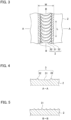
- FIG. 3 is an enlarged top view of a part of the scale-like portion
- FIG. 4 is a sectional view cut at a part indicated by A-A in FIG. 3
- FIG. 5 is a sectional view cut at a part indicated by B-B in FIG. 3
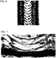
- FIG. 6 and FIG. 7 are scanning electron microscope photographs showing the structure of the scale-like portion.
- the scale-like portion 3 is obtained by deforming the surface of the lead frame 2 into a scaly shape by consecutively applying a laser beam as a spot on the lead frame 2, and is formed in a given straight line with a predetermined width W as shown in FIG. 3 .
- an arrow denoted by L represents the longitudinal direction of the scale-like portion 3.
- the scale-like portion 3 includes a scale portion 31 on which scale-shaped projections are consecutively provided, and ridge portions 32 provided on both sides of the scale portion 31 in parallel to the longitudinal direction L of the scale-like portion 3. As shown in FIG. 7 , the ridge portions 32 are raised to be higher than the scale portion 31 and an area between the two ridge portions 32 has a groove shape.
- the width W and the height of the scale-like portion 3 can be adjusted using laser output, scan speed, and the like.
- the width W of the scale-like portion 3 is set to about 60 um to 600 um, for example. The greater the width W of the scale-like portion 3 is, the higher the void inhibition effect is.
- the scale-like portion 3 is formed through laser application, the scale-like portion 3 can be easily formed at any location on the lead frame 2, and the flatness of the lead frame 2 is not lost during the working. It is also easy to selectively process only a part where the scale-like portion 3 is to be provided while avoiding a part where the scale-like portion 3 is not to be provided, e.g., a wire connection portion or the like. In addition, the scale-like portion 3 may be provided in a curved line. Further, if the scale-like portion 3 is formed by a unicursal processing pattern, the takt time can be shortened and productivity is improved.
- the scale-like portions 3 are arranged such that the longitudinal direction L of the scale-like portions 3 is perpendicular to the resin boundary portion 2b.
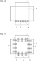
- the scale-like portions 3 are arranged such that the longitudinal direction L of the scale-like portions 3 is parallel to the resin boundary portion 2b. As shown in FIG. 10 and FIG.
- the width W of each scale-like portion 3 is set to be great (for example, about 600 um) so as to ensure that the scale-like portion 3 is formed across the resin boundary portion 2b.
- a plurality of (here, four) scale-like portions 3 are provided across the resin boundary portion 2b at a part to which the straight distance from the gate breaking trace 8b is longest on the lead frame 2.
- a plurality of scale-like portions 3 are provided at intervals on the resin boundary portion 2b on the side opposite to the side surface having the gate breaking trace 8b.
- a plurality of scale-like portions 3 are provided at intervals over the entire areas of the resin boundary portions 2b on the four sides of the rectangular module. It is noted that, although the scale-like portions 3 are arranged at equal intervals in FIG. 11 , the scale-like portions 3 do not necessarily need to be arranged at equal intervals, and may be closely arranged at a part where a void is likely to occur. Using the configurations as shown in FIG. 11 and FIG. 12 can cope with voids at every part inside the molding resin 8.
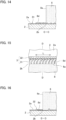
- FIG. 13 is an enlarged top view of a part of the semiconductor device in the case where the longitudinal direction of the scale-like portion is perpendicular to the resin boundary portion
- FIG. 14 is a sectional view cut at a part indicated by C-C in FIG. 13
- FIG. 15 is an enlarged top view of a part of the semiconductor device in the case where the longitudinal direction of the scale-like portion is parallel to the resin boundary portion
- FIG. 16 is a sectional view cut at a part indicated by D-D in FIG. 15 .
- the surface of the lead frame 2 is coated with the metal plating 2a, and the scale-like portion 3 is formed on the metal plating 2a.
- Copper which is the material of the lead frame 2 is readily oxidized, and cost is required for management of the oxidation degree if the lead frame 2 is in an exposed state. Therefore, if the scale-like portion 3 is formed with the metal plating 2a remaining on the surface of the lead frame 2, copper oxidation degree management becomes easy.
- laser working is easier for the metal plating 2a such as nickel, as compared to copper which has a high reflectance for a laser beam.
- the scale-like portion 3 may be formed at both of the metal plating 2a and the lead frame 2 under the metal plating 2a. That is, the lead frame 2 may be exposed or deformed at the scale-like portion 3. In any case, a void inhibition effect can be obtained in accordance with the dimensions in width W, height, and longitudinal direction L of the scale-like portion 3.
- the width of the resin leakage 8d can be kept within a narrow range equal to the width W of the scale-like portion.
- the resin leakage 8d in the direction (vertical direction in FIG. 15 ) perpendicular to the longitudinal direction L is inhibited by the ridge portion 32.
- the range of the resin leakage 8d can be kept within a short distance from the resin boundary portion 2b to the ridge portion 32.
- the arrangement relationship is appropriately selected in accordance with the condition around the part where the scale-like portion 3 is provided.
- transfer molding is used for the resin sealing process.
- the manufacturing method for the semiconductor device 100 is not limited thereto.
- injection molding may be used, which can contribute to cost reduction for resin.
- the scale-like portion 3 is provided over both sides across the resin boundary portion 2b on the lead frame 2, whereby air present inside the molding resin can be discharged to the outside of the mold 20 in the resin sealing process, thus providing a void inhibition effect. Since the scale-like portion 3 is formed by applying a laser beam to the lead frame 2, it is possible to easily provide the scale-like portion 3 at a part where a void is likely to occur, and flatness of the lead frame 2 is not lost during working. Further, working for providing an air vent in the mold is not needed, and a void can be coped with at low cost. Thus, according to embodiment 1, the semiconductor device 100 having a high function and high reliability can be obtained at low cost.
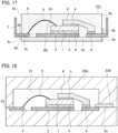
- FIG. 17 is a sectional view showing a semiconductor device according to embodiment 2
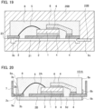
- FIG. 18 is a sectional view showing a first-time transfer molding process for the semiconductor device according to embodiment 2
- FIG. 19 is a sectional view showing a second-time transfer molding process for the semiconductor device according to embodiment 2.
- a semiconductor device 101 according to embodiment 2 includes a first resin (hereinafter, molding resin 8) and a second resin (hereinafter, second molding resin 9).
- the lead frame 2 of the semiconductor device 101 has a mounting portion 2A on which the semiconductor element 1 is mounted, and a heat dissipation portion 2B opposite to the mounting portion 2A.
- the mounting portion 2A is sealed by the molding resin 8, and the heat dissipation portion 2B is sealed by the second molding resin 9.
- a scale-like portion 3b is provided over both sides across a resin boundary portion 2c of an area sealed by the second molding resin 9 on the heat dissipation portion 2B.
- a thin molding portion 9d having a thickness of about 0.02 mm to 0.3 mm is formed on the heat dissipation portion 2B of the lead frame 2, a thin molding portion 9d having a thickness of about 0.02 mm to 0.3 mm is formed.
- the thin molding portion 9d is joined to a heatsink made of copper or aluminum, via a heat dissipation member such as grease.
- the molding resin 8 and the second molding resin 9 are both made from thermosetting epoxy resin or the like. It is noted that, for the second molding resin 9 on the heat dissipation portion 2B side, a high-heat-dissipation resin having a higher thermal conductivity than the molding resin 8 is used. The thermal conductivity of the second molding resin 9 is 3 W/m ⁇ K to 12 W/m-K. For the molding resin 8 on the mounting portion 2A side, a low-stress resin which is a molding resin for a general integrated circuit is used.
- Manufacturing of the semiconductor device 101 includes two times of transfer molding processes. As shown in FIG. 18 , in the first-time transfer molding process, the lead frame 2 on which the semiconductor element 1 and the like are mounted is placed inside a first mold 20A, and the cavity 21 is present on the mounting portion 2A side of the lead frame 2. A melted molding resin is injected into the cavity 21 of the first mold 20A through an upper gate 22A.
- the molding resin flows on the mounting portion side of the lead frame 2 to fill the cavity 21.
- the molded product is taken out from the first mold 20A, and immediately after this, a gate breaking process for separating a runner 8c from the molded product is performed.
- the gate breaking trace 8b (see FIG. 17 ) remains at the side surface 8a of the molding resin 8.
- the second-time transfer molding process is performed.
- a UV treatment or a plasma treatment may be performed on the molding resin 8 after the first-time transfer molding process.
- FIG. 19 inside a second mold 20B used in the second-time transfer molding process, the lead frame 2 of which the mounting portion 2A side has been sealed through the first-time transfer molding process is placed, and the cavity 21 is present on the heat dissipation portion 2B side of the lead frame 2.
- the melted second molding resin is injected into the cavity 21 through a lower gate 22B.
- the second molding resin flows into the cavity 21 to form the thin molding portion 9d and flows to the scale-like portion 3b.
- the second molding resin flowing on the scale-like portion 3b forms a discharge path for air owing to recesses/projections on the scale-like portion 3b, whereby air is discharged through the abutting surfaces 23 of the second mold 20B.
- the molded product is taken out from the second mold 20B, and immediately after this, a gate breaking process of separating a runner 9c from the molded product is performed. After the gate breaking, a gate breaking trace 9b (see FIG. 17 ) remains at a side surface 9a of the second molding resin 9.
- the thin molding portion 9d covering the heat dissipation portion 2B of the lead frame 2 is a thin high-heat-dissipation resin which is excellent in heat dissipation property, but has a high flow resistance during molding and thus is poor in fluidity, so that a void due to air entrapment is likely to occur.
- a void can be effectively inhibited by providing the scale-like portion 3b on the heat dissipation portion 2B side, whereby the semiconductor device 101 which is excellent in heat dissipation property and has a high function and high reliability can be obtained at low cost.
- a scale-like portion 3a may be provided at the resin boundary portion 2b of the area sealed by the molding resin 8 on the mounting portion 2A, whereby the same effects as in the above embodiment 1 can be obtained.
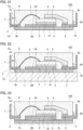
- a semiconductor device having an insulation adhesion member on the heat dissipation portion 2B side of the lead frame 2 will be described with reference to FIG. 21 to FIG. 23 .
- the mounting portion 2A of the lead frame 2 is sealed by the molding resin 8, and an insulation adhesion member 10 is provided on the heat dissipation portion 2B.
- a heatsink 11 is provided on the heat dissipation portion 2B of the lead frame 2 with an insulation adhesion member 10 interposed therebetween.
- the insulation adhesion member 10 is made of mainly epoxy resin, ceramic, silicone, or the like, and is a high-thermal-conductivity member having a thermal conductivity of 1 W/m ⁇ K to 15 W/m ⁇ K.
- a sheet-like member may be used or a liquid insulation adhesion member may be cured and used.
- a void can occur at a pasted surface of the insulation adhesion member 10 due to air entrapment at the time of pasting.
- a void due to gas of a solvent or the like separated from the adhesive agent during the curing process can occur inside the insulation adhesion member 10. Both of the above cases can cause reduction in electric insulation property, moisture-proof property, heat dissipation property, and adhesion property. Therefore, a void needs to be inhibited and it is effective to provide the scale-like portion 3b.
- the scale-like portion 3a is provided over both sides across the resin boundary portion 2b on the mounting portion 2A of the lead frame 2.
- the function of the scale-like portion 3a is the same as in the above embodiment 1 and therefore description thereof is omitted.
- the scale-like portion 3b is provided over both sides across an insulation adhesion member boundary portion 2d which is the boundary between the inside and the outside of an area covered by the insulation adhesion member 10 on the heat dissipation portion 2B of the lead frame 2.
- the thickness of the lead frame 2 differs between the part where the semiconductor element 1 is mounted and the part having the external terminal 7. Therefore, around the heat dissipation portion 2B of the lead frame 2, the molding resin 8 is flush with the heat dissipation portion 2B. Further, the insulation adhesion member 10 is provided on the heat dissipation portion 2B and the molding resin 8 being flush with the heat dissipation portion 2B. In this case, merely providing the scale-like portion on the heat dissipation portion 2B side of the lead frame 2 cannot obtain a void inhibition effect.
- a scale-like portion 3c is formed continuously to the end of the molding resin 8, i.e., the side surface 8a from the heat dissipation portion 2B of the lead frame 2 covered by the insulation adhesion member 10.
- air inside the insulation adhesion member 10 or at the pasted surface thereof can be discharged, whereby a void inhibition effect is obtained.
- the scale-like portion 3c can be formed by one-time processing without changing the laser application condition between the heat dissipation portion 2B of the lead frame 2 and the molding resin 8.
- the heatsink 11 may be provided on the heat dissipation portion 2B of the semiconductor device 104 shown in FIG. 23 , with the insulation adhesion member 10 interposed therebetween. Providing the heatsink 11 obtains a semiconductor device having a small interfacial thermal resistance and excellent heat dissipation property. It is noted that a glass epoxy substrate or the like may be provided on the heat dissipation portion 2B of the lead frame 2 with the insulation adhesion member 10 interposed therebetween.
Landscapes
- Encapsulation Of And Coatings For Semiconductor Or Solid State Devices (AREA)
- Structures Or Materials For Encapsulating Or Coating Semiconductor Devices Or Solid State Devices (AREA)
Claims (14)
- Dispositif à semi-conducteur comprenant :une grille de connexion (2) sur laquelle est monté un élément semi-conducteur (1) et qui est constituée de métal ; etune résine (8, 9) scellant, de la grille de connexion (2), au moins une surface sur laquelle l'élément semi-conducteur (1) est monté, dans lequella grille de connexion (2) présente une partie (3, 3a, 3b) en forme d'échelle sur laquelle des saillies en forme d'échelle sont formées consécutivement,dans lequel la partie (3, 3a, 3b) en forme d'échelle est disposée sur les deux côtés à travers une partie (2b, 2c) de délimitation de résine qui est une délimitation entre l'intérieur et l'extérieur d'une zone scellée par la résine (8, 9) sur la grille de connexion (2) ;caractérisé en ce quela partie (3) en forme d'échelle inclut une partie en échelle (31) sur laquelle les saillies en forme d'échelle sont disposées consécutivement, et des parties crête (32) disposées des deux côtés de la partie en échelle (31).
- Dispositif à semi-conducteur selon la revendication 1, dans lequel
une pluralité de parties (3) en forme d'échelle sont disposées à des intervalles les unes des autres. - Dispositif à semi-conducteur selon la revendication 1 ou la revendication 2, dans lequel
la partie (3) en forme d'échelle est disposée en ligne droite, et une direction longitudinale de la partie (3) en forme d'échelle est perpendiculaire à la partie (2b) de délimitation de résine. - Dispositif à semi-conducteur selon la revendication 1 ou la revendication 2, dans lequel
la partie (3) en forme d'échelle est disposée en ligne droite, et une direction longitudinale de la partie (3) en forme d'échelle est parallèle à la partie (2b) de délimitation de résine. - Dispositif à semi-conducteur selon l'une quelconque des revendications 1 à 4, dans lequel
la résine (8) présente une trace (8b) de rupture de grille au niveau d'une partie d'une surface latérale (8a) de celle-ci, et la partie (3) en forme d'échelle est disposée au niveau de la partie (2b) de délimitation de résine au niveau de laquelle une distance en ligne droite depuis la trace (8b) de rupture de grille est la plus longue. - Dispositif à semi-conducteur selon l'une quelconque des revendications 1 à 4, dans lequel
la résine (8) présente une trace (8b) de rupture de grille au niveau d'une partie d'une surface latérale (8a) de celle-ci, et la partie (3) en forme d'échelle est disposée au niveau de la partie (2b) de délimitation de résine sur un côté opposé à la surface latérale (8a) présentant la trace (8b) de rupture de grille. - Dispositif à semi-conducteur selon l'une quelconque des revendications 1 à 4, dans lequel
la partie (3) en forme d'échelle est disposée sur toute une surface de la partie (2b) de délimitation de résine. - Dispositif à semi-conducteur selon l'une quelconque des revendications 1 à 7, comprenant un placage métallique (2a) recouvrant une partie ou la totalité d'une surface de la grille de connexion (2), dans lequel
la partie (3) en forme d'échelle est formée au niveau du placage métallique (2a). - Dispositif à semi-conducteur selon l'une quelconque des revendications 1 à 7, comprenant un placage métallique (2a) recouvrant une partie ou la totalité d'une surface de la grille de connexion (2), dans lequel
la partie (3) en forme d'échelle est formée au niveau du placage métallique (2a) et de la grille de connexion (2). - Dispositif à semi-conducteur selon l'une quelconque des revendications 1 à 9, dans lequella grille de connexion (2) présente une partie de montage (2A) sur laquelle l'élément semi-conducteur (1) est monté, et une partie de dissipation de chaleur (2B) opposée à la partie de montage (2A),la résine (8, 9) inclut une première résine (8) scellant la partie de montage (2A) et une seconde résine (9) scellant la partie de dissipation de chaleur (2B), et la partie de dissipation de chaleur (2B) est pourvue d'une partie (9d) de moulage mince formée par la seconde résine (9), etla partie (3b) en forme d'échelle est disposée sur les deux côtés à travers la partie de délimitation de résine (2c) d'une zone scellée par la seconde résine (9) sur la partie de dissipation de chaleur (2B).
- Dispositif à semi-conducteur selon la revendication 10, dans lequel
la partie (3a) en forme d'échelle est disposée sur les deux côtés à travers la partie (2b) de délimitation de résine d'une zone scellée par la première résine (8) sur la partie de montage (2A). - Dispositif à semi-conducteur selon l'une quelconque des revendications 1 à 9, dans lequella grille de connexion (2) présente une partie de montage (2A) sur laquelle l'élément semi-conducteur (1) est monté, et une partie de dissipation de chaleur (2B) opposée à la partie de montage (2A),la partie de dissipation de chaleur (2B) est pourvue d'un élément d'adhérence d'isolation (10), etla partie (3b) en forme d'échelle est disposée sur les deux côtés à travers une partie de délimitation d'élément d'adhérence d'isolation (2d) qui est une délimitation entre l'intérieur et l'extérieur d'une zone recouverte par l'élément d'adhérence d'isolation (10) sur la grille de connexion (2).
- Dispositif à semi-conducteur selon l'une quelconque des revendications 1 à 9, dans lequella grille de connexion (2) présente une partie de montage (2A) sur laquelle l'élément semi-conducteur (1) est monté, et une partie de dissipation de chaleur (2B) opposée à la partie de montage (2A),un élément d'adhérence d'isolation (10) est disposé sur la partie de dissipation de chaleur (2B) et la résine (8) affleure la partie de dissipation de chaleur (2B), etla partie (3c) en forme d'échelle est disposée en continu à une extrémité de la résine (8) depuis la partie de dissipation de chaleur (2B) recouverte par l'élément d'adhérence d'isolation (10).
- Dispositif à semi-conducteur selon la revendication 12 ou la revendication 13, dans lequel
un dissipateur thermique (11) est disposé sur la partie de dissipation de chaleur (2B) de la grille de connexion (2) avec l'élément d'adhérence d'isolation (10) interposé entre ceux-ci.
Applications Claiming Priority (1)
| Application Number | Priority Date | Filing Date | Title |
|---|---|---|---|
| PCT/JP2018/032965 WO2020049672A1 (fr) | 2018-09-06 | 2018-09-06 | Dispositif à semi-conducteur |
Publications (3)
| Publication Number | Publication Date |
|---|---|
| EP3848961A1 EP3848961A1 (fr) | 2021-07-14 |
| EP3848961A4 EP3848961A4 (fr) | 2021-09-22 |
| EP3848961B1 true EP3848961B1 (fr) | 2024-09-18 |
Family
ID=69721896
Family Applications (1)
| Application Number | Title | Priority Date | Filing Date |
|---|---|---|---|
| EP18932539.2A Active EP3848961B1 (fr) | 2018-09-06 | 2018-09-06 | Dispositif à semi-conducteur |
Country Status (5)
| Country | Link |
|---|---|
| US (1) | US11837516B2 (fr) |
| EP (1) | EP3848961B1 (fr) |
| JP (1) | JP7090716B2 (fr) |
| CN (1) | CN112640096A (fr) |
| WO (1) | WO2020049672A1 (fr) |
Families Citing this family (3)
| Publication number | Priority date | Publication date | Assignee | Title |
|---|---|---|---|---|
| WO2021199635A1 (fr) * | 2020-03-30 | 2021-10-07 | ローム株式会社 | Dispositif à semi-conducteur |
| US20220102231A1 (en) * | 2020-09-25 | 2022-03-31 | Intel Corporation | Dummy die in a recessed mold structure of a packaged integrated circuit device |
| CN114334674B (zh) * | 2021-08-16 | 2026-03-31 | 华为数字能源技术有限公司 | 功率半导体模块制备方法及功率半导体模块 |
Family Cites Families (17)
| Publication number | Priority date | Publication date | Assignee | Title |
|---|---|---|---|---|
| JPS59109155U (ja) * | 1983-01-12 | 1984-07-23 | 日本電気ホームエレクトロニクス株式会社 | 電子部品 |
| JP2893085B2 (ja) | 1988-10-18 | 1999-05-17 | トーワ株式会社 | 電子部品の樹脂封止成形方法及び装置 |
| JPH09321205A (ja) * | 1996-05-29 | 1997-12-12 | Hitachi Ltd | 半導体装置の製造方法およびその方法で用いるリードフレームならびにリードフレームの製造方法 |
| JP3740116B2 (ja) * | 2002-11-11 | 2006-02-01 | 三菱電機株式会社 | モールド樹脂封止型パワー半導体装置及びその製造方法 |
| JP2006049698A (ja) * | 2004-08-06 | 2006-02-16 | Denso Corp | 樹脂封止型半導体装置 |
| JP2006303215A (ja) * | 2005-04-21 | 2006-11-02 | Denso Corp | 樹脂封止型半導体装置 |
| US20090146280A1 (en) * | 2005-11-28 | 2009-06-11 | Dai Nippon Printing Co., Ltd. | Circuit member, manufacturing method of the circuit member, and semiconductor device including the circuit member |
| US8410601B2 (en) * | 2009-11-15 | 2013-04-02 | Microsemi Corporation | RF package |
| CN106471617B (zh) * | 2014-04-04 | 2019-05-10 | 三菱电机株式会社 | 半导体装置 |
| EP3285288B1 (fr) * | 2015-04-15 | 2021-03-31 | Mitsubishi Electric Corporation | Dispositif à semi-conducteur |
| EP3929974A1 (fr) | 2015-04-15 | 2021-12-29 | Mitsubishi Electric Corporation | Dispositif à semiconducteurs |
| JP2017055044A (ja) * | 2015-09-11 | 2017-03-16 | 古河電気工業株式会社 | リードフレーム |
| WO2017154072A1 (fr) | 2016-03-07 | 2017-09-14 | 三菱電機株式会社 | Dispositif à semi-conducteurs et procédé de fabrication de dispositif à semi-conducteurs |
| DE102016109349A1 (de) * | 2016-05-20 | 2017-11-23 | Infineon Technologies Ag | Chipgehäuse, verfahren zum bilden eines chipgehäuses und verfahren zum bilden eines elektrischen kontakts |
| KR102232994B1 (ko) * | 2017-02-21 | 2021-03-26 | 미쓰비시덴키 가부시키가이샤 | 반도체 장치 |
| EP3686925B1 (fr) * | 2017-09-21 | 2021-08-04 | Mitsubishi Electric Corporation | Dispositif à semi-conducteur et dispositif de conversion de puissance qui en est doté |
| US10658278B2 (en) * | 2018-08-16 | 2020-05-19 | Texas Instruments Incorporated | Electrical device terminal finishing |
-
2018
- 2018-09-06 EP EP18932539.2A patent/EP3848961B1/fr active Active
- 2018-09-06 JP JP2020540933A patent/JP7090716B2/ja active Active
- 2018-09-06 WO PCT/JP2018/032965 patent/WO2020049672A1/fr not_active Ceased
- 2018-09-06 US US17/256,841 patent/US11837516B2/en active Active
- 2018-09-06 CN CN201880097013.1A patent/CN112640096A/zh active Pending
Also Published As
| Publication number | Publication date |
|---|---|
| EP3848961A4 (fr) | 2021-09-22 |
| US11837516B2 (en) | 2023-12-05 |
| US20210305111A1 (en) | 2021-09-30 |
| EP3848961A1 (fr) | 2021-07-14 |
| JP7090716B2 (ja) | 2022-06-24 |
| JPWO2020049672A1 (ja) | 2021-08-12 |
| CN112640096A (zh) | 2021-04-09 |
| WO2020049672A1 (fr) | 2020-03-12 |
Similar Documents
| Publication | Publication Date | Title |
|---|---|---|
| KR101645771B1 (ko) | 반도체 장치 및 그 제조 방법 | |
| EP3128550A1 (fr) | Dispositif semi-conducteur | |
| US6593169B2 (en) | Method of making hybrid integrated circuit device | |
| JP6345342B2 (ja) | 半導体装置 | |
| JP7504258B2 (ja) | 半導体製造装置およびそれを用いた半導体装置の製造方法ならびに半導体装置 | |
| KR20100039293A (ko) | 양면 냉각 집적전력장치 패키지 및 모듈과 그의 제조 방법 | |
| JP6266168B2 (ja) | 半導体装置 | |
| CN104051397B (zh) | 包括非整数引线间距的封装器件及其制造方法 | |
| CN104218013A (zh) | 半导体装置以及半导体装置的制造方法 | |
| KR101378792B1 (ko) | 클립리스 및 와이어리스 반도체 다이 패키지 및 그제조방법 | |
| EP3428962B1 (fr) | Dispositif à semi-conducteurs et procédé de fabrication de dispositif à semi-conducteurs | |
| JP7845824B2 (ja) | 半導体装置 | |
| EP3848961B1 (fr) | Dispositif à semi-conducteur | |
| JP7594950B2 (ja) | 半導体装置 | |
| JP2022143167A (ja) | 半導体装置 | |
| EP4184566B1 (fr) | Dispositif à semi-conducteur et procédé de fabrication d'un tel dispositif à semi-conducteur | |
| CN205319149U (zh) | 半导体封装体 | |
| JP7135293B2 (ja) | 半導体装置および半導体装置の製造方法 | |
| US20250385162A1 (en) | Semiconductor device assemblies with wettable die attach area and associated methods | |
| EP3869540A1 (fr) | Dispositif à semi-conducteur de puissance et son procédé de fabrication | |
| KR20240155794A (ko) | 반도체 패키지 내 기판에 전력 단자를 연결하는 방법 | |
| CN119008430A (zh) | 半导体装置封装互连及其制造方法 |
Legal Events
| Date | Code | Title | Description |
|---|---|---|---|
| STAA | Information on the status of an ep patent application or granted ep patent |
Free format text: STATUS: THE INTERNATIONAL PUBLICATION HAS BEEN MADE |
|
| PUAI | Public reference made under article 153(3) epc to a published international application that has entered the european phase |
Free format text: ORIGINAL CODE: 0009012 |
|
| STAA | Information on the status of an ep patent application or granted ep patent |
Free format text: STATUS: REQUEST FOR EXAMINATION WAS MADE |
|
| 17P | Request for examination filed |
Effective date: 20210112 |
|
| AK | Designated contracting states |
Kind code of ref document: A1 Designated state(s): AL AT BE BG CH CY CZ DE DK EE ES FI FR GB GR HR HU IE IS IT LI LT LU LV MC MK MT NL NO PL PT RO RS SE SI SK SM TR |
|
| A4 | Supplementary search report drawn up and despatched |
Effective date: 20210819 |
|
| RIC1 | Information provided on ipc code assigned before grant |
Ipc: H01L 23/495 20060101ALI20210813BHEP Ipc: H01L 23/31 20060101ALI20210813BHEP Ipc: H01L 21/48 20060101ALI20210813BHEP Ipc: H01L 23/50 20060101ALI20210813BHEP Ipc: H01L 23/28 20060101ALI20210813BHEP Ipc: H01L 21/56 20060101ALI20210813BHEP Ipc: H01L 23/48 20060101AFI20210813BHEP |
|
| DAV | Request for validation of the european patent (deleted) | ||
| DAX | Request for extension of the european patent (deleted) | ||
| GRAP | Despatch of communication of intention to grant a patent |
Free format text: ORIGINAL CODE: EPIDOSNIGR1 |
|
| STAA | Information on the status of an ep patent application or granted ep patent |
Free format text: STATUS: GRANT OF PATENT IS INTENDED |
|
| INTG | Intention to grant announced |
Effective date: 20240425 |
|
| GRAS | Grant fee paid |
Free format text: ORIGINAL CODE: EPIDOSNIGR3 |
|
| GRAA | (expected) grant |
Free format text: ORIGINAL CODE: 0009210 |
|
| STAA | Information on the status of an ep patent application or granted ep patent |
Free format text: STATUS: THE PATENT HAS BEEN GRANTED |
|
| AK | Designated contracting states |
Kind code of ref document: B1 Designated state(s): AL AT BE BG CH CY CZ DE DK EE ES FI FR GB GR HR HU IE IS IT LI LT LU LV MC MK MT NL NO PL PT RO RS SE SI SK SM TR |
|
| REG | Reference to a national code |
Ref country code: GB Ref legal event code: FG4D |
|
| REG | Reference to a national code |
Ref country code: CH Ref legal event code: EP |
|
| REG | Reference to a national code |
Ref country code: IE Ref legal event code: FG4D |
|
| REG | Reference to a national code |
Ref country code: DE Ref legal event code: R096 Ref document number: 602018074628 Country of ref document: DE |
|
| REG | Reference to a national code |
Ref country code: LT Ref legal event code: MG9D |
|
| PG25 | Lapsed in a contracting state [announced via postgrant information from national office to epo] |
Ref country code: NO Free format text: LAPSE BECAUSE OF FAILURE TO SUBMIT A TRANSLATION OF THE DESCRIPTION OR TO PAY THE FEE WITHIN THE PRESCRIBED TIME-LIMIT Effective date: 20241218 |
|
| PG25 | Lapsed in a contracting state [announced via postgrant information from national office to epo] |
Ref country code: GR Free format text: LAPSE BECAUSE OF FAILURE TO SUBMIT A TRANSLATION OF THE DESCRIPTION OR TO PAY THE FEE WITHIN THE PRESCRIBED TIME-LIMIT Effective date: 20241219 Ref country code: FI Free format text: LAPSE BECAUSE OF FAILURE TO SUBMIT A TRANSLATION OF THE DESCRIPTION OR TO PAY THE FEE WITHIN THE PRESCRIBED TIME-LIMIT Effective date: 20240918 |
|
| PG25 | Lapsed in a contracting state [announced via postgrant information from national office to epo] |
Ref country code: BG Free format text: LAPSE BECAUSE OF FAILURE TO SUBMIT A TRANSLATION OF THE DESCRIPTION OR TO PAY THE FEE WITHIN THE PRESCRIBED TIME-LIMIT Effective date: 20240918 |
|
| PG25 | Lapsed in a contracting state [announced via postgrant information from national office to epo] |
Ref country code: LV Free format text: LAPSE BECAUSE OF FAILURE TO SUBMIT A TRANSLATION OF THE DESCRIPTION OR TO PAY THE FEE WITHIN THE PRESCRIBED TIME-LIMIT Effective date: 20240918 |
|
| PG25 | Lapsed in a contracting state [announced via postgrant information from national office to epo] |
Ref country code: HR Free format text: LAPSE BECAUSE OF FAILURE TO SUBMIT A TRANSLATION OF THE DESCRIPTION OR TO PAY THE FEE WITHIN THE PRESCRIBED TIME-LIMIT Effective date: 20240918 |
|
| REG | Reference to a national code |
Ref country code: NL Ref legal event code: MP Effective date: 20240918 |
|
| PG25 | Lapsed in a contracting state [announced via postgrant information from national office to epo] |
Ref country code: RS Free format text: LAPSE BECAUSE OF FAILURE TO SUBMIT A TRANSLATION OF THE DESCRIPTION OR TO PAY THE FEE WITHIN THE PRESCRIBED TIME-LIMIT Effective date: 20241218 |
|
| PG25 | Lapsed in a contracting state [announced via postgrant information from national office to epo] |
Ref country code: RS Free format text: LAPSE BECAUSE OF FAILURE TO SUBMIT A TRANSLATION OF THE DESCRIPTION OR TO PAY THE FEE WITHIN THE PRESCRIBED TIME-LIMIT Effective date: 20241218 Ref country code: NO Free format text: LAPSE BECAUSE OF FAILURE TO SUBMIT A TRANSLATION OF THE DESCRIPTION OR TO PAY THE FEE WITHIN THE PRESCRIBED TIME-LIMIT Effective date: 20241218 Ref country code: LV Free format text: LAPSE BECAUSE OF FAILURE TO SUBMIT A TRANSLATION OF THE DESCRIPTION OR TO PAY THE FEE WITHIN THE PRESCRIBED TIME-LIMIT Effective date: 20240918 Ref country code: HR Free format text: LAPSE BECAUSE OF FAILURE TO SUBMIT A TRANSLATION OF THE DESCRIPTION OR TO PAY THE FEE WITHIN THE PRESCRIBED TIME-LIMIT Effective date: 20240918 Ref country code: GR Free format text: LAPSE BECAUSE OF FAILURE TO SUBMIT A TRANSLATION OF THE DESCRIPTION OR TO PAY THE FEE WITHIN THE PRESCRIBED TIME-LIMIT Effective date: 20241219 Ref country code: FI Free format text: LAPSE BECAUSE OF FAILURE TO SUBMIT A TRANSLATION OF THE DESCRIPTION OR TO PAY THE FEE WITHIN THE PRESCRIBED TIME-LIMIT Effective date: 20240918 Ref country code: BG Free format text: LAPSE BECAUSE OF FAILURE TO SUBMIT A TRANSLATION OF THE DESCRIPTION OR TO PAY THE FEE WITHIN THE PRESCRIBED TIME-LIMIT Effective date: 20240918 |
|
| REG | Reference to a national code |
Ref country code: AT Ref legal event code: MK05 Ref document number: 1725440 Country of ref document: AT Kind code of ref document: T Effective date: 20240918 |
|
| PG25 | Lapsed in a contracting state [announced via postgrant information from national office to epo] |
Ref country code: NL Free format text: LAPSE BECAUSE OF FAILURE TO SUBMIT A TRANSLATION OF THE DESCRIPTION OR TO PAY THE FEE WITHIN THE PRESCRIBED TIME-LIMIT Effective date: 20240918 |
|
| PG25 | Lapsed in a contracting state [announced via postgrant information from national office to epo] |
Ref country code: PT Free format text: LAPSE BECAUSE OF FAILURE TO SUBMIT A TRANSLATION OF THE DESCRIPTION OR TO PAY THE FEE WITHIN THE PRESCRIBED TIME-LIMIT Effective date: 20250120 Ref country code: IS Free format text: LAPSE BECAUSE OF FAILURE TO SUBMIT A TRANSLATION OF THE DESCRIPTION OR TO PAY THE FEE WITHIN THE PRESCRIBED TIME-LIMIT Effective date: 20250118 |
|
| PG25 | Lapsed in a contracting state [announced via postgrant information from national office to epo] |
Ref country code: RO Free format text: LAPSE BECAUSE OF FAILURE TO SUBMIT A TRANSLATION OF THE DESCRIPTION OR TO PAY THE FEE WITHIN THE PRESCRIBED TIME-LIMIT Effective date: 20240918 Ref country code: SM Free format text: LAPSE BECAUSE OF FAILURE TO SUBMIT A TRANSLATION OF THE DESCRIPTION OR TO PAY THE FEE WITHIN THE PRESCRIBED TIME-LIMIT Effective date: 20240918 |
|
| PG25 | Lapsed in a contracting state [announced via postgrant information from national office to epo] |
Ref country code: ES Free format text: LAPSE BECAUSE OF FAILURE TO SUBMIT A TRANSLATION OF THE DESCRIPTION OR TO PAY THE FEE WITHIN THE PRESCRIBED TIME-LIMIT Effective date: 20240918 |
|
| PG25 | Lapsed in a contracting state [announced via postgrant information from national office to epo] |
Ref country code: EE Free format text: LAPSE BECAUSE OF FAILURE TO SUBMIT A TRANSLATION OF THE DESCRIPTION OR TO PAY THE FEE WITHIN THE PRESCRIBED TIME-LIMIT Effective date: 20240918 Ref country code: AT Free format text: LAPSE BECAUSE OF FAILURE TO SUBMIT A TRANSLATION OF THE DESCRIPTION OR TO PAY THE FEE WITHIN THE PRESCRIBED TIME-LIMIT Effective date: 20240918 |
|
| PG25 | Lapsed in a contracting state [announced via postgrant information from national office to epo] |
Ref country code: PL Free format text: LAPSE BECAUSE OF FAILURE TO SUBMIT A TRANSLATION OF THE DESCRIPTION OR TO PAY THE FEE WITHIN THE PRESCRIBED TIME-LIMIT Effective date: 20240918 Ref country code: CZ Free format text: LAPSE BECAUSE OF FAILURE TO SUBMIT A TRANSLATION OF THE DESCRIPTION OR TO PAY THE FEE WITHIN THE PRESCRIBED TIME-LIMIT Effective date: 20240918 |
|
| PG25 | Lapsed in a contracting state [announced via postgrant information from national office to epo] |
Ref country code: IT Free format text: LAPSE BECAUSE OF FAILURE TO SUBMIT A TRANSLATION OF THE DESCRIPTION OR TO PAY THE FEE WITHIN THE PRESCRIBED TIME-LIMIT Effective date: 20240918 Ref country code: SK Free format text: LAPSE BECAUSE OF FAILURE TO SUBMIT A TRANSLATION OF THE DESCRIPTION OR TO PAY THE FEE WITHIN THE PRESCRIBED TIME-LIMIT Effective date: 20240918 |
|
| REG | Reference to a national code |
Ref country code: DE Ref legal event code: R097 Ref document number: 602018074628 Country of ref document: DE |
|
| PG25 | Lapsed in a contracting state [announced via postgrant information from national office to epo] |
Ref country code: DK Free format text: LAPSE BECAUSE OF FAILURE TO SUBMIT A TRANSLATION OF THE DESCRIPTION OR TO PAY THE FEE WITHIN THE PRESCRIBED TIME-LIMIT Effective date: 20240918 |
|
| PLBE | No opposition filed within time limit |
Free format text: ORIGINAL CODE: 0009261 |
|
| STAA | Information on the status of an ep patent application or granted ep patent |
Free format text: STATUS: NO OPPOSITION FILED WITHIN TIME LIMIT |
|
| 26N | No opposition filed |
Effective date: 20250619 |
|
| PG25 | Lapsed in a contracting state [announced via postgrant information from national office to epo] |
Ref country code: SE Free format text: LAPSE BECAUSE OF FAILURE TO SUBMIT A TRANSLATION OF THE DESCRIPTION OR TO PAY THE FEE WITHIN THE PRESCRIBED TIME-LIMIT Effective date: 20240918 |
|
| P01 | Opt-out of the competence of the unified patent court (upc) registered |
Free format text: CASE NUMBER: UPC_APP_4937_3848961/2025 Effective date: 20250827 |
|
| PGFP | Annual fee paid to national office [announced via postgrant information from national office to epo] |
Ref country code: DE Payment date: 20250730 Year of fee payment: 8 |
|
| PGFP | Annual fee paid to national office [announced via postgrant information from national office to epo] |
Ref country code: FR Payment date: 20250808 Year of fee payment: 8 |
|
| REG | Reference to a national code |
Ref country code: DE Ref legal event code: R079 Ref document number: 602018074628 Country of ref document: DE Free format text: PREVIOUS MAIN CLASS: H01L0023480000 Ipc: H10W0072000000 |