WO2020049672A1 - Dispositif à semi-conducteur - Google Patents
Dispositif à semi-conducteur Download PDFInfo
- Publication number
- WO2020049672A1 WO2020049672A1 PCT/JP2018/032965 JP2018032965W WO2020049672A1 WO 2020049672 A1 WO2020049672 A1 WO 2020049672A1 JP 2018032965 W JP2018032965 W JP 2018032965W WO 2020049672 A1 WO2020049672 A1 WO 2020049672A1
- Authority
- WO
- WIPO (PCT)
- Prior art keywords
- resin
- scale
- semiconductor device
- lead frame
- heat radiating
- Prior art date
- Legal status (The legal status is an assumption and is not a legal conclusion. Google has not performed a legal analysis and makes no representation as to the accuracy of the status listed.)
- Ceased
Links
Images









Classifications
-
- H—ELECTRICITY
- H10—SEMICONDUCTOR DEVICES; ELECTRIC SOLID-STATE DEVICES NOT OTHERWISE PROVIDED FOR
- H10W—GENERIC PACKAGES, INTERCONNECTIONS, CONNECTORS OR OTHER CONSTRUCTIONAL DETAILS OF DEVICES COVERED BY CLASS H10
- H10W74/00—Encapsulations, e.g. protective coatings
- H10W74/10—Encapsulations, e.g. protective coatings characterised by their shape or disposition
-
- H—ELECTRICITY
- H10—SEMICONDUCTOR DEVICES; ELECTRIC SOLID-STATE DEVICES NOT OTHERWISE PROVIDED FOR
- H10W—GENERIC PACKAGES, INTERCONNECTIONS, CONNECTORS OR OTHER CONSTRUCTIONAL DETAILS OF DEVICES COVERED BY CLASS H10
- H10W70/00—Package substrates; Interposers; Redistribution layers [RDL]
- H10W70/40—Leadframes
- H10W70/421—Shapes or dispositions
- H10W70/424—Cross-sectional shapes
-
- H—ELECTRICITY
- H10—SEMICONDUCTOR DEVICES; ELECTRIC SOLID-STATE DEVICES NOT OTHERWISE PROVIDED FOR
- H10W—GENERIC PACKAGES, INTERCONNECTIONS, CONNECTORS OR OTHER CONSTRUCTIONAL DETAILS OF DEVICES COVERED BY CLASS H10
- H10W40/00—Arrangements for thermal protection or thermal control
- H10W40/20—Arrangements for cooling
- H10W40/22—Arrangements for cooling characterised by their shape, e.g. having conical or cylindrical projections
- H10W40/226—Arrangements for cooling characterised by their shape, e.g. having conical or cylindrical projections characterised by projecting parts, e.g. fins to increase surface area
- H10W40/228—Arrangements for cooling characterised by their shape, e.g. having conical or cylindrical projections characterised by projecting parts, e.g. fins to increase surface area the projecting parts being wire-shaped or pin-shaped
-
- H—ELECTRICITY
- H10—SEMICONDUCTOR DEVICES; ELECTRIC SOLID-STATE DEVICES NOT OTHERWISE PROVIDED FOR
- H10W—GENERIC PACKAGES, INTERCONNECTIONS, CONNECTORS OR OTHER CONSTRUCTIONAL DETAILS OF DEVICES COVERED BY CLASS H10
- H10W70/00—Package substrates; Interposers; Redistribution layers [RDL]
- H10W70/01—Manufacture or treatment
- H10W70/04—Manufacture or treatment of leadframes
-
- H—ELECTRICITY
- H10—SEMICONDUCTOR DEVICES; ELECTRIC SOLID-STATE DEVICES NOT OTHERWISE PROVIDED FOR
- H10W—GENERIC PACKAGES, INTERCONNECTIONS, CONNECTORS OR OTHER CONSTRUCTIONAL DETAILS OF DEVICES COVERED BY CLASS H10
- H10W70/00—Package substrates; Interposers; Redistribution layers [RDL]
- H10W70/40—Leadframes
- H10W70/461—Leadframes specially adapted for cooling
-
- H—ELECTRICITY
- H10—SEMICONDUCTOR DEVICES; ELECTRIC SOLID-STATE DEVICES NOT OTHERWISE PROVIDED FOR
- H10W—GENERIC PACKAGES, INTERCONNECTIONS, CONNECTORS OR OTHER CONSTRUCTIONAL DETAILS OF DEVICES COVERED BY CLASS H10
- H10W74/00—Encapsulations, e.g. protective coatings
- H10W74/01—Manufacture or treatment
- H10W74/016—Manufacture or treatment using moulds
-
- H—ELECTRICITY
- H10—SEMICONDUCTOR DEVICES; ELECTRIC SOLID-STATE DEVICES NOT OTHERWISE PROVIDED FOR
- H10W—GENERIC PACKAGES, INTERCONNECTIONS, CONNECTORS OR OTHER CONSTRUCTIONAL DETAILS OF DEVICES COVERED BY CLASS H10
- H10W74/00—Encapsulations, e.g. protective coatings
- H10W74/10—Encapsulations, e.g. protective coatings characterised by their shape or disposition
- H10W74/111—Encapsulations, e.g. protective coatings characterised by their shape or disposition the semiconductor body being completely enclosed
-
- H—ELECTRICITY
- H10—SEMICONDUCTOR DEVICES; ELECTRIC SOLID-STATE DEVICES NOT OTHERWISE PROVIDED FOR
- H10W—GENERIC PACKAGES, INTERCONNECTIONS, CONNECTORS OR OTHER CONSTRUCTIONAL DETAILS OF DEVICES COVERED BY CLASS H10
- H10W74/00—Encapsulations, e.g. protective coatings
- H10W74/10—Encapsulations, e.g. protective coatings characterised by their shape or disposition
- H10W74/111—Encapsulations, e.g. protective coatings characterised by their shape or disposition the semiconductor body being completely enclosed
- H10W74/127—Encapsulations, e.g. protective coatings characterised by their shape or disposition the semiconductor body being completely enclosed characterised by arrangements for sealing or adhesion
-
- H—ELECTRICITY
- H10—SEMICONDUCTOR DEVICES; ELECTRIC SOLID-STATE DEVICES NOT OTHERWISE PROVIDED FOR
- H10W—GENERIC PACKAGES, INTERCONNECTIONS, CONNECTORS OR OTHER CONSTRUCTIONAL DETAILS OF DEVICES COVERED BY CLASS H10
- H10W70/00—Package substrates; Interposers; Redistribution layers [RDL]
- H10W70/40—Leadframes
- H10W70/456—Materials
- H10W70/457—Materials of metallic layers on leadframes
-
- H—ELECTRICITY
- H10—SEMICONDUCTOR DEVICES; ELECTRIC SOLID-STATE DEVICES NOT OTHERWISE PROVIDED FOR
- H10W—GENERIC PACKAGES, INTERCONNECTIONS, CONNECTORS OR OTHER CONSTRUCTIONAL DETAILS OF DEVICES COVERED BY CLASS H10
- H10W72/00—Interconnections or connectors in packages
- H10W72/071—Connecting or disconnecting
- H10W72/075—Connecting or disconnecting of bond wires
-
- H—ELECTRICITY
- H10—SEMICONDUCTOR DEVICES; ELECTRIC SOLID-STATE DEVICES NOT OTHERWISE PROVIDED FOR
- H10W—GENERIC PACKAGES, INTERCONNECTIONS, CONNECTORS OR OTHER CONSTRUCTIONAL DETAILS OF DEVICES COVERED BY CLASS H10
- H10W72/00—Interconnections or connectors in packages
- H10W72/071—Connecting or disconnecting
- H10W72/076—Connecting or disconnecting of strap connectors
-
- H—ELECTRICITY
- H10—SEMICONDUCTOR DEVICES; ELECTRIC SOLID-STATE DEVICES NOT OTHERWISE PROVIDED FOR
- H10W—GENERIC PACKAGES, INTERCONNECTIONS, CONNECTORS OR OTHER CONSTRUCTIONAL DETAILS OF DEVICES COVERED BY CLASS H10
- H10W72/00—Interconnections or connectors in packages
- H10W72/30—Die-attach connectors
- H10W72/351—Materials of die-attach connectors
- H10W72/352—Materials of die-attach connectors comprising metals or metalloids, e.g. solders
-
- H—ELECTRICITY
- H10—SEMICONDUCTOR DEVICES; ELECTRIC SOLID-STATE DEVICES NOT OTHERWISE PROVIDED FOR
- H10W—GENERIC PACKAGES, INTERCONNECTIONS, CONNECTORS OR OTHER CONSTRUCTIONAL DETAILS OF DEVICES COVERED BY CLASS H10
- H10W72/00—Interconnections or connectors in packages
- H10W72/50—Bond wires
- H10W72/551—Materials of bond wires
- H10W72/552—Materials of bond wires comprising metals or metalloids, e.g. silver
-
- H—ELECTRICITY
- H10—SEMICONDUCTOR DEVICES; ELECTRIC SOLID-STATE DEVICES NOT OTHERWISE PROVIDED FOR
- H10W—GENERIC PACKAGES, INTERCONNECTIONS, CONNECTORS OR OTHER CONSTRUCTIONAL DETAILS OF DEVICES COVERED BY CLASS H10
- H10W72/00—Interconnections or connectors in packages
- H10W72/50—Bond wires
- H10W72/551—Materials of bond wires
- H10W72/552—Materials of bond wires comprising metals or metalloids, e.g. silver
- H10W72/5522—Materials of bond wires comprising metals or metalloids, e.g. silver comprising gold [Au]
-
- H—ELECTRICITY
- H10—SEMICONDUCTOR DEVICES; ELECTRIC SOLID-STATE DEVICES NOT OTHERWISE PROVIDED FOR
- H10W—GENERIC PACKAGES, INTERCONNECTIONS, CONNECTORS OR OTHER CONSTRUCTIONAL DETAILS OF DEVICES COVERED BY CLASS H10
- H10W72/00—Interconnections or connectors in packages
- H10W72/50—Bond wires
- H10W72/551—Materials of bond wires
- H10W72/552—Materials of bond wires comprising metals or metalloids, e.g. silver
- H10W72/5524—Materials of bond wires comprising metals or metalloids, e.g. silver comprising aluminium [Al]
-
- H—ELECTRICITY
- H10—SEMICONDUCTOR DEVICES; ELECTRIC SOLID-STATE DEVICES NOT OTHERWISE PROVIDED FOR
- H10W—GENERIC PACKAGES, INTERCONNECTIONS, CONNECTORS OR OTHER CONSTRUCTIONAL DETAILS OF DEVICES COVERED BY CLASS H10
- H10W72/00—Interconnections or connectors in packages
- H10W72/50—Bond wires
- H10W72/551—Materials of bond wires
- H10W72/552—Materials of bond wires comprising metals or metalloids, e.g. silver
- H10W72/5525—Materials of bond wires comprising metals or metalloids, e.g. silver comprising copper [Cu]
-
- H—ELECTRICITY
- H10—SEMICONDUCTOR DEVICES; ELECTRIC SOLID-STATE DEVICES NOT OTHERWISE PROVIDED FOR
- H10W—GENERIC PACKAGES, INTERCONNECTIONS, CONNECTORS OR OTHER CONSTRUCTIONAL DETAILS OF DEVICES COVERED BY CLASS H10
- H10W72/00—Interconnections or connectors in packages
- H10W72/60—Strap connectors, e.g. thick copper clips for grounding of power devices
- H10W72/641—Dispositions of strap connectors
- H10W72/646—Dispositions of strap connectors the connected ends being on auxiliary connecting means on bond pads, e.g. on a bump connector
-
- H—ELECTRICITY
- H10—SEMICONDUCTOR DEVICES; ELECTRIC SOLID-STATE DEVICES NOT OTHERWISE PROVIDED FOR
- H10W—GENERIC PACKAGES, INTERCONNECTIONS, CONNECTORS OR OTHER CONSTRUCTIONAL DETAILS OF DEVICES COVERED BY CLASS H10
- H10W72/00—Interconnections or connectors in packages
- H10W72/60—Strap connectors, e.g. thick copper clips for grounding of power devices
- H10W72/651—Materials of strap connectors
- H10W72/652—Materials of strap connectors comprising metals or metalloids, e.g. silver
-
- H—ELECTRICITY
- H10—SEMICONDUCTOR DEVICES; ELECTRIC SOLID-STATE DEVICES NOT OTHERWISE PROVIDED FOR
- H10W—GENERIC PACKAGES, INTERCONNECTIONS, CONNECTORS OR OTHER CONSTRUCTIONAL DETAILS OF DEVICES COVERED BY CLASS H10
- H10W72/00—Interconnections or connectors in packages
- H10W72/851—Dispositions of multiple connectors or interconnections
- H10W72/853—On the same surface
- H10W72/871—Bond wires and strap connectors
-
- H—ELECTRICITY
- H10—SEMICONDUCTOR DEVICES; ELECTRIC SOLID-STATE DEVICES NOT OTHERWISE PROVIDED FOR
- H10W—GENERIC PACKAGES, INTERCONNECTIONS, CONNECTORS OR OTHER CONSTRUCTIONAL DETAILS OF DEVICES COVERED BY CLASS H10
- H10W72/00—Interconnections or connectors in packages
- H10W72/851—Dispositions of multiple connectors or interconnections
- H10W72/874—On different surfaces
- H10W72/884—Die-attach connectors and bond wires
-
- H—ELECTRICITY
- H10—SEMICONDUCTOR DEVICES; ELECTRIC SOLID-STATE DEVICES NOT OTHERWISE PROVIDED FOR
- H10W—GENERIC PACKAGES, INTERCONNECTIONS, CONNECTORS OR OTHER CONSTRUCTIONAL DETAILS OF DEVICES COVERED BY CLASS H10
- H10W72/00—Interconnections or connectors in packages
- H10W72/851—Dispositions of multiple connectors or interconnections
- H10W72/874—On different surfaces
- H10W72/886—Die-attach connectors and strap connectors
-
- H—ELECTRICITY
- H10—SEMICONDUCTOR DEVICES; ELECTRIC SOLID-STATE DEVICES NOT OTHERWISE PROVIDED FOR
- H10W—GENERIC PACKAGES, INTERCONNECTIONS, CONNECTORS OR OTHER CONSTRUCTIONAL DETAILS OF DEVICES COVERED BY CLASS H10
- H10W72/00—Interconnections or connectors in packages
- H10W72/90—Bond pads, in general
- H10W72/951—Materials of bond pads
- H10W72/952—Materials of bond pads comprising metals or metalloids, e.g. PbSn, Ag or Cu
-
- H—ELECTRICITY
- H10—SEMICONDUCTOR DEVICES; ELECTRIC SOLID-STATE DEVICES NOT OTHERWISE PROVIDED FOR
- H10W—GENERIC PACKAGES, INTERCONNECTIONS, CONNECTORS OR OTHER CONSTRUCTIONAL DETAILS OF DEVICES COVERED BY CLASS H10
- H10W74/00—Encapsulations, e.g. protective coatings
-
- H—ELECTRICITY
- H10—SEMICONDUCTOR DEVICES; ELECTRIC SOLID-STATE DEVICES NOT OTHERWISE PROVIDED FOR
- H10W—GENERIC PACKAGES, INTERCONNECTIONS, CONNECTORS OR OTHER CONSTRUCTIONAL DETAILS OF DEVICES COVERED BY CLASS H10
- H10W90/00—Package configurations
- H10W90/701—Package configurations characterised by the relative positions of pads or connectors relative to package parts
- H10W90/731—Package configurations characterised by the relative positions of pads or connectors relative to package parts of die-attach connectors
- H10W90/736—Package configurations characterised by the relative positions of pads or connectors relative to package parts of die-attach connectors between a chip and a stacked lead frame, conducting package substrate or heat sink
-
- H—ELECTRICITY
- H10—SEMICONDUCTOR DEVICES; ELECTRIC SOLID-STATE DEVICES NOT OTHERWISE PROVIDED FOR
- H10W—GENERIC PACKAGES, INTERCONNECTIONS, CONNECTORS OR OTHER CONSTRUCTIONAL DETAILS OF DEVICES COVERED BY CLASS H10
- H10W90/00—Package configurations
- H10W90/701—Package configurations characterised by the relative positions of pads or connectors relative to package parts
- H10W90/751—Package configurations characterised by the relative positions of pads or connectors relative to package parts of bond wires
- H10W90/756—Package configurations characterised by the relative positions of pads or connectors relative to package parts of bond wires between a chip and a stacked lead frame, conducting package substrate or heat sink
-
- H—ELECTRICITY
- H10—SEMICONDUCTOR DEVICES; ELECTRIC SOLID-STATE DEVICES NOT OTHERWISE PROVIDED FOR
- H10W—GENERIC PACKAGES, INTERCONNECTIONS, CONNECTORS OR OTHER CONSTRUCTIONAL DETAILS OF DEVICES COVERED BY CLASS H10
- H10W90/00—Package configurations
- H10W90/701—Package configurations characterised by the relative positions of pads or connectors relative to package parts
- H10W90/761—Package configurations characterised by the relative positions of pads or connectors relative to package parts of strap connectors
- H10W90/766—Package configurations characterised by the relative positions of pads or connectors relative to package parts of strap connectors between a chip and a stacked lead frame, conducting package substrate or heat sink
Definitions
- the present application relates to a resin mold type semiconductor device.
- voids may also occur in the high heat conductive insulating adhesive member disposed between the heat radiating portion and the heat sink of the semiconductor device.
- voids are generated between the insulating adhesive member and the lead frame due to the entrainment of air at the time of sticking.
- voids are generated due to a solvent gas separated from the adhesive during the curing process. In any case, the presence of the voids causes a decrease in electrical insulation, moisture resistance, heat dissipation, and adhesion, thereby reducing the function of the semiconductor device.
- the present application discloses a technique for solving the above-described problem, and provides a high-performance, high-reliability, and low-cost semiconductor device that suppresses a void generated in a mold resin or an insulating adhesive member.
- the purpose is to do.
- the semiconductor device disclosed in the present application is a metal lead frame on which a semiconductor element is mounted, and a semiconductor device including a resin that seals at least a surface of the lead frame on which the semiconductor element is mounted.
- the scaly protrusion has a continuously formed scaly portion, and the scaly portion is disposed on both sides of a resin boundary portion which is a boundary between the inside and the outside of the region sealed by the resin of the lead frame. Things.
- FIG. 2 is a sectional view showing the semiconductor device according to the first embodiment
- FIG. 5 is a cross-sectional view showing a transfer molding step of the semiconductor device according to the first embodiment.
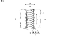
- FIG. 3 is a top view showing a scale-like portion in the semiconductor device according to the first embodiment;
- FIG. 3 is a cross-sectional view illustrating a scale portion in the semiconductor device according to the first embodiment;
- FIG. 3 is a cross-sectional view illustrating a scale portion in the semiconductor device according to the first embodiment;
- FIG. 4 is a diagram by a scanning electron micrograph showing a form of a scale in the semiconductor device according to the first embodiment;
- FIG. 4 is a diagram by a scanning electron micrograph showing a form of a scale in the semiconductor device according to the first embodiment;
- FIG. 4 is a diagram by a scanning electron micrograph showing a form of a scale in the semiconductor device according to the first embodiment;
- FIG. 4 is a diagram by a scanning electron micrograph showing a form
- FIG. 4 is a diagram showing an example of the arrangement of the scales in the semiconductor device according to the first embodiment;
- FIG. 4 is a diagram showing an example of the arrangement of the scales in the semiconductor device according to the first embodiment;
- FIG. 4 is a diagram showing an example of the arrangement of the scales in the semiconductor device according to the first embodiment;
- FIG. 4 is a diagram showing an example of the arrangement of the scales in the semiconductor device according to the first embodiment;
- FIG. 4 is a diagram showing an example of the arrangement of the scales in the semiconductor device according to the first embodiment;
- FIG. 5 is a top view illustrating functions of the scale-like portion in the semiconductor device according to the first embodiment;
- FIG. 4 is a cross-sectional view illustrating a function of a scale-like portion in the semiconductor device according to the first embodiment
- FIG. 5 is a top view illustrating functions of the scale-like portion in the semiconductor device according to the first embodiment
- FIG. 4 is a cross-sectional view illustrating a function of a scale-like portion in the semiconductor device according to the first embodiment
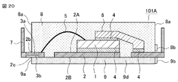
- FIG. 14 is a cross-sectional view showing a semiconductor device according to a second embodiment.
- FIG. 15 is a cross-sectional view showing a first transfer molding step of the semiconductor device according to the second embodiment.
- FIG. 15 is a cross-sectional view showing a second transfer molding step of the semiconductor device according to the second embodiment.
- FIG. 14 is a sectional view showing another semiconductor device according to the second embodiment.
- FIG. 14 is a sectional view showing a semiconductor device according to a third embodiment.
- FIG. 14 is a sectional view showing another semiconductor device according to the third embodiment.
- FIG. 15 is a cross-
- FIG. 1 is a cross-sectional view illustrating the semiconductor device according to the first embodiment
- FIG. 2 is a cross-sectional view illustrating a transfer molding process of the semiconductor device according to the first embodiment.
- the semiconductor device 100 according to the first embodiment includes a semiconductor element 1, a lead frame 2, wires 5 and inner leads 6, which are wiring members, external terminals 7, a molding resin 8, and the like.
- the same or corresponding parts have the same reference characters allotted.
- the semiconductor element 1 is, for example, an insulated gate bipolar transistor (IGBT), a metal oxide film field effect transistor (MOSFET), an IC chip, an LSI chip, or the like. 4 is implemented. Note that components (not shown) other than the semiconductor element 1 are also mounted on the mounting portion of the lead frame 2.
- IGBT insulated gate bipolar transistor
- MOSFET metal oxide film field effect transistor
- the lead frame 2 is made of a copper plate or a copper alloy plate.
- the surface of the lead frame 2 may be coated with a metal plating 2a of gold, silver, nickel, tin, or the like for the purpose of improving corrosion resistance and heat resistance, and nickel is often used.
- the lead frame 2 has a scale portion 3 in which scale-like projections are continuously formed.
- the scaly portions 3 are arranged on both sides of a resin boundary portion 2b, which is a boundary between the inside and the outside of the region sealed by the mold resin 8 of the lead frame 2. The scale 3 will be described later in detail.
- the electrode pads of the semiconductor element 1 are connected to the external terminals 7 via the wires 5 connected by wire bonding or the inner leads 6 made of a copper plate or a copper alloy plate.
- the wire 5 and the inner lead 6 can be replaced with each other.
- the wire 5 is made of gold, silver, aluminum, copper, or the like, and has a wire diameter of about 20 ⁇ m to 500 ⁇ m.
- a mold resin 8 which is a resin such as a thermosetting epoxy resin.
- both surfaces of the lead frame 2 are sealed with one type of mold resin 8.
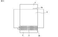
- the molded resin 8 molded into a substantially rectangular parallelepiped has a gate break mark 8b on a part of the side surface 8a, and the scale 3 is disposed on the resin boundary 2b on the side facing the side surface 8a having the gate break mark 8b. Have been.
- the transfer molding process of the semiconductor device 100 according to the first embodiment will be described with reference to FIG.
- the lead frame 2 on which the semiconductor element 1 and the like are mounted is installed inside the molding die 20, and the molten molding resin is injected into the cavity 21 of the molding die 20 through the gate 22.
- the clearance between the external terminal 7 and the molding die 20 is very narrow so that a large amount of the molding resin 8 does not leak from the molding die 20.
- the portion having the longest linear distance from the gate break mark 8b of the semiconductor device 100 (the opposite side of the gate break mark 8b in the case of a rectangular module) is the final filling point of the mold resin. Since the mold resin 8 flows into the final filling place in a state where the viscosity is high and the wettability is deteriorated, voids are easily generated in the final filling place due to the entrainment of air.
- the semiconductor device 100 includes, as void suppression means in the mold resin 8, the scale 3 disposed so as to straddle the resin boundary 2 b of the lead frame 2.
- the scale 3 reaches the mating surface 23 of the upper mold and the lower mold of the molding die 20.
- the mold resin flowing into the scale portion 3 has an air escape path due to the unevenness of the scale portion 3, and the air escapes from the mating surface 23 of the molding die 20.
- the air passage formed in the mold resin disappears when the mold resin is completely cured.
- the mold resin remaining in the gate 22 is called a runner 8c.
- a gate break is performed to separate the semiconductor device 100 from the runner 8c.
- Gate break marks 8b remain on the side surface 8a of the mold resin 8 after the gate break.
- FIG. 3 is a top view showing a scale-like portion partially enlarged
- FIG. 4 is a cross-sectional view taken along a line AA in FIG. 3
- FIG. 5 is a portion taken along a line BB in FIG. It is sectional drawing which cut
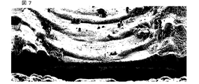
- 6 and 7 are scanning electron micrographs showing the form of the scale.
- the scaly portion 3 is formed by deforming the surface of the lead frame 2 into a scaly shape by continuously irradiating the spot to the lead frame 2 with a laser, and as shown in FIG. W is arranged.
- the arrow indicated by L indicates the longitudinal direction of the scale 3.
- the scale portion 3 has a scale portion 31 on which scale-like protrusions are continuously arranged, and a raised portion 32 arranged on both sides of the scale portion 31 in parallel with the longitudinal direction L of the scale portion 3. As shown in FIG. 7, the raised portion 32 is raised higher than the scale portion 31, and a groove is formed between the two raised portions 32.
- the width W and height of the scale 3 can be adjusted by the output of the laser, the scanning speed, and the like.
- the width W of the scale portion 3 is set, for example, to about 60 ⁇ m to 600 ⁇ m. The larger the width W of the scale 3 is, the higher the void suppressing effect is.
- the scaly portion 3 is formed by laser irradiation, it can be easily formed at an arbitrary position on the lead frame 2 and does not impair the flatness of the lead frame 2 during processing. It is also easy to selectively process only the portion where the scaly portion 3 is to be arranged, and avoid the portion where the scaly portion 3 is not arranged, for example, the wire connection portion.
- the scale 3 may be arranged on a curve. Furthermore, by making the processing pattern of the scale 3 a single stroke, the tact time can be reduced and the productivity is improved.
- the scaly portion 3 is very effective against such a situation, and the scaly portion 3 may be arranged at a location where it is found that voids are likely to occur. This eliminates the need for processing of a molding die, and can be implemented at low cost.
- FIGS. 8, 9 and 11 An example of the arrangement of the scaly portion 3 and its effect will be described with reference to FIGS.
- the longitudinal direction L of the scale 3 and the resin boundary 2b are arranged perpendicularly.
- the longitudinal direction L of the scale 3 and the resin boundary 2b are arranged in parallel.
- the scale portion 3 is placed in the resin boundary portion 2b in consideration of a displacement (about 200 ⁇ m at the maximum) during laser processing.
- the width W of the scale 3 is set large (for example, about 600 ⁇ m) so as to securely straddle.
- a plurality of (four in this case) scale-like portions 3 are arranged so as to straddle the resin boundary portion 2b where the linear distance is the longest from the gate break mark 8b of the lead frame 2.
- a plurality of scales 3 are arranged at intervals on the resin boundary 2b on the side facing the side surface having the gate break mark 8b. 8 to FIG. 10, it is possible to suppress voids near the final filling position of the mold resin.
- a plurality of scales 3 are arranged at intervals over the entire area of the resin boundary 2b on the four sides of the rectangular module.
- the scales 3 are arranged at equal intervals. However, they do not need to be at equal intervals, and may be densely arranged at locations where voids are likely to occur.
- voids in all parts inside the mold resin 8 can be dealt with.
- FIG. 13 is a partially enlarged top view showing a semiconductor device in which the longitudinal direction of the scaly portion and the resin boundary portion are arranged vertically
- FIG. 14 is a cross-sectional view taken along a line CC of FIG. is there.
- FIG. 15 is a partially enlarged top view showing a semiconductor device in which the longitudinal direction of the scaly portion and the resin boundary portion are arranged in parallel
- FIG. 16 is a cross section cut along a line DD in FIG. FIG.
- the surface of the lead frame 2 is covered with the metal plating 2a, and the scale 3 is formed with the metal plating 2a.
- Copper which is a material of the lead frame 2, is easily oxidized, and the cost of managing the degree of oxidation in an exposed state is high. Therefore, by forming the scale portion 3 with the metal plating 2a left on the surface of the lead frame 2, it is easy to control the degree of oxidation of copper. Further, compared with copper having a high laser reflectance, the metal plating 2a such as nickel is easier to laser-process.
- the scale 3 When the scale 3 is formed on the lead frame 2 covered with the metal plating 2a, the scale 3 may be formed on both the metal plating 2a and the lead frame 2 therebelow. That is, in the scale 3, the lead frame 2 may be exposed or deformed. In any case, a void suppression effect according to the width W, the height, and the dimension of the scale portion 3 in the longitudinal direction L can be obtained.
- the upper and lower mating surfaces 23 of the molding die 20 are sealed so that no resin leaks. At this time, if the seal is loose, resin leakage occurs, and unnecessary resin burrs are formed. Unnecessary resin burrs adversely affect tie bar cutting, lead forming, and the like in the subsequent steps, and require an additional step of removing resin burrs, which is not desirable.
- a resin leak 8 d (a region indicated by a dot in the figure) occurs within the range of the scale 3.
- the scale-like portion 3 is disposed at a position where there is no functional problem even if the resin leakage 8d occurs.
- the amount of resin leakage in the scale portion 3 varies depending on the molding pressure, the shape of the scale portion 3, and the like.
- the resin leakage 8d generated in the scale portion 3 remains in the scale portion 3 and spreads to a portion other than the scale portion 3. Therefore, the adverse effects described above are unlikely to occur.
- the resin leakage 8d in a direction perpendicular to the longitudinal direction L (vertical direction in FIG. 15).
- the range of the resin leakage 8d can be suppressed to a short distance from the resin boundary portion 2b to the raised portion 32.
- the range of the resin leakage 8d changes depending on the arrangement of the longitudinal direction L of the scale portion 3 and the resin boundary portion 2b. Therefore, the range of the resin leakage 8d is appropriately selected according to the situation around the place where the scale portion 3 is arranged.
- the transfer molding method is adopted as the resin sealing step, but the method of manufacturing the semiconductor device 100 is not limited to this.
- an injection molding method may be used, and in that case, it is possible to contribute to cost reduction of the resin.
- the scale-like portions 3 As described above, according to the first embodiment, by disposing the scale-like portions 3 on both sides of the resin boundary portion 2b of the lead frame 2, air existing inside the mold resin in the resin sealing step is reduced. It can be pulled out of the mold 20, and the effect of suppressing voids can be obtained. Since the scaly portion 3 is formed by irradiating the lead frame 2 with a laser, the scale portion 3 can be easily arranged at a location where voids are easily generated, and the flatness of the lead frame 2 is not impaired at the time of processing. Further, it is not necessary to provide an air vent in the molding die, and it is possible to cope at a low cost. From these facts, according to the first embodiment, a high-performance, high-reliability, and low-cost semiconductor device 100 can be obtained.
- FIG. 17 is a cross-sectional view illustrating a semiconductor device according to the second embodiment
- FIG. 18 is a cross-sectional view illustrating a first transfer molding step of the semiconductor device according to the second embodiment
- FIG. FIG. 11 is a cross-sectional view showing a second transfer molding step of the semiconductor device.
- the semiconductor device 101 according to the second embodiment includes a first resin (hereinafter, a molding resin 8) and a second resin (hereinafter, a second molding resin 9).
- the lead frame 2 of the semiconductor device 101 has a mounting portion 2A on which the semiconductor element 1 is mounted, and a heat radiating portion 2B opposed to the mounting portion 2A.
- the mounting portion 2A is sealed with a mold resin 8, and the heat radiating portion 2B Are sealed by a second mold resin 9.
- the scaly portions 3b are arranged on both sides of the resin boundary portion 2c of the region of the heat radiation portion 2B sealed by the second mold resin 9.
- a thin molded section 9d having a thickness of about 0.02 mm to about 0.3 mm is molded.
- the thin molded portion 9d is joined to a heat sink made of copper or aluminum via a heat radiating member such as grease.
- Both the mold resin 8 and the second mold resin 9 are thermosetting epoxy resins or the like. However, as the second mold resin 9 on the heat radiating portion 2B side, a high heat radiating resin having a higher thermal conductivity than the mold resin 8 is used. The thermal conductivity of the second mold resin 9 is 3 W / m ⁇ K to 12 W / m ⁇ K. As the molding resin 8 on the mounting portion 2A side, a low-stress resin, which is a molding resin for a general integrated circuit, is used.
- the transfer molding process of the semiconductor device 101 according to the second embodiment will be described with reference to FIGS.
- the semiconductor device 101 is manufactured including two transfer molding steps. As shown in FIG. 18, in the first transfer molding step, the lead frame 2 on which the semiconductor element 1 and the like are mounted is installed inside the first molding die 20A, and the mounting portion 2A side of the lead frame 2 is hollow. It is 21. The molten mold resin is injected into the cavity 21 of the first molding die 20A through the upper gate 22A.
- the mold resin flows toward the mounting portion side of the lead frame 2 and fills the cavity 21.
- a gate break step of separating the runner 8c from the molded article is performed. After the gate break, a gate break mark 8b (see FIG. 17) remains on the side surface 8a of the mold resin 8.
- the second transfer molding step is performed.
- the mold resin 8 may be subjected to a UV treatment or a plasma treatment in order to enhance the adhesion between the mold resin 8 and the second mold resin 9.
- the lead frame 2 in which the mounting portion 2A side is sealed after the first transfer molding step is installed inside the second molding die 20B used in the second transfer molding step.
- the heat radiating portion 2B side of the lead frame 2 is a cavity 21.
- the melted second mold resin is injected into the cavity 21 through the lower gate 22B.
- the second mold resin flows into the cavity 21 to form the thin-walled molded portion 9d and to flow into the scale portion 3b.
- the second mold resin that has flowed into the scale portion 3b has an air escape path due to the unevenness of the scale portion 3b, and the air escapes from the mating surface 23 of the second molding die 20B.
- a gate break process of separating the runner 9c from the molded product is performed. After the gate break, a gate break mark 9b (see FIG. 17) remains on the side surface 9a of the second mold resin 9.
- the thin molded portion 9d covering the heat radiating portion 2B of the lead frame 2 is made of a thin high heat radiating resin and has excellent heat radiating properties. It's easy to do.
- the second embodiment by arranging scale-like portion 3b on the side of heat radiating portion 2B, voids can be effectively suppressed, and a high-performance, high-reliability, and low-cost semiconductor device having excellent heat radiation properties. 101 is obtained.
- the scale portion 3a may be arranged at the resin boundary portion 2b in the region sealed by the mold resin 8 of the mounting portion 2A. The same effect as in the first embodiment can be obtained.
- Embodiment 3 a semiconductor device having an insulating adhesive member on the heat radiating portion 2B side of the lead frame 2 will be described with reference to FIGS.
- the mounting portion 2A of the lead frame 2 is sealed with the mold resin 8, and the heat radiation portion 2B is provided with the insulating adhesive member 10.
- a heat sink 11 is provided on a heat radiating portion 2 ⁇ / b> B of the lead frame 2 via an insulating adhesive member 10.
- the insulating adhesive member 10 is a high heat conductive member having a thermal conductivity of 1 W / m ⁇ K to 15 W / m ⁇ K, mainly containing epoxy resin, ceramic, silicone or the like.
- the insulating adhesive member 10 there are a sheet-like member and a member that is used by curing a liquid insulating adhesive member.
- voids may be generated on the attaching surface of the insulating adhesive member 10 due to the entrainment of air at the time of attachment.
- a void caused by a gas such as a solvent separated from the adhesive during the curing process may be generated inside the insulating adhesive member 10. In any case, it is necessary to suppress voids because electrical insulation, moisture resistance, heat dissipation, and adhesion are reduced, and the scale portion 3b is effective.
- scale parts 3a are arranged on both sides of the resin boundary part 2b of the mounting part 2A of the lead frame 2.
- the function of the scale portion 3a is the same as that of the first embodiment, and the description is omitted.
- scale portions 3b are arranged on both sides of the insulating adhesive member boundary 2d which is a boundary between the inside and the outside of the area covered by the insulating adhesive member 10 of the heat radiating portion 2B of the lead frame 2.
- the thickness of the lead frame 2 is different between a place where the semiconductor element 1 is mounted and a place where the external terminal 7 is provided. For this reason, around the heat radiating portion 2B of the lead frame 2, the mold resin 8 forms the same surface as the heat radiating portion 2B. Further, an insulating adhesive member 10 is provided on the heat radiating portion 2B and the mold resin 8 which is on the same surface as the heat radiating portion 2B. In such a case, the effect of suppressing voids cannot be obtained simply by disposing the scaly portion on the heat radiating portion 2B side of the lead frame 2.
- the scale portions 3c are continuously arranged from the heat radiating portion 2B of the lead frame 2 covered with the insulating adhesive member 10 to the end of the mold resin 8, that is, the side surface 8a. Thereby, the air inside the insulating adhesive member 10 or the bonding surface can be evacuated, and the effect of suppressing voids can be obtained.
- the scale-like portion 3c can be formed by a single process without changing the laser irradiation conditions between the heat radiating portion 2B of the lead frame 2 and the mold resin 8. Alternatively, it is also possible to switch the irradiation program in one process and process the heat radiating section 2B and the mold resin 8 under different irradiation conditions.
- a heat sink 11 may be provided on the heat radiating portion 2B of the semiconductor device 104 shown in FIG. By providing the heat sink 11, a semiconductor device having low interface thermal resistance and excellent heat dissipation can be obtained.
- a glass epoxy substrate or the like is provided on the heat radiating portion 2B of the lead frame 2 via the insulating adhesive member 10.
- the insulating adhesive member 10 is provided on the heat radiating portion 2B side of the lead frame 2, it is possible to suppress voids in the insulating adhesive member 10 by the scale portions 3b and 3c.
- semiconductor devices 102, 103, and 104 having high performance, high reliability, and low cost with excellent heat dissipation can be obtained.
Landscapes
- Encapsulation Of And Coatings For Semiconductor Or Solid State Devices (AREA)
- Structures Or Materials For Encapsulating Or Coating Semiconductor Devices Or Solid State Devices (AREA)
Abstract
L'invention concerne une grille de connexion (2) de ce dispositif à semi-conducteur (101) qui a une partie de moule à paroi mince (9d) d'épaisseur d'environ 0,02 à 0,3 mm formée sur une unité de rayonnement de chaleur (2B) opposée à une unité de montage (2A) sur laquelle est chargé un élément semi-conducteur (1), à l'aide d'une seconde résine de moule (9) qui est une résine à rayonnement thermique élevé. Une partie en forme d'échelle (3b) sur laquelle des saillies en forme d'échelle sont formées de façon continue est placée sur les deux côtés prenant en sandwich une partie de délimitation de résine (2c) de l'unité de rayonnement de chaleur (2B). La partie en forme d'échelle (3b) atteint le moule supérieur et des surfaces d'accouplement de moule inférieures du moule métallique de moulage utilisé dans l'étape de moulage, et le même type d'effet de suppression de vide qu'un évent d'air est ainsi obtenu.
Priority Applications (5)
| Application Number | Priority Date | Filing Date | Title |
|---|---|---|---|
| PCT/JP2018/032965 WO2020049672A1 (fr) | 2018-09-06 | 2018-09-06 | Dispositif à semi-conducteur |
| US17/256,841 US11837516B2 (en) | 2018-09-06 | 2018-09-06 | Semiconductor device |
| EP18932539.2A EP3848961B1 (fr) | 2018-09-06 | 2018-09-06 | Dispositif à semi-conducteur |
| JP2020540933A JP7090716B2 (ja) | 2018-09-06 | 2018-09-06 | 半導体装置 |
| CN201880097013.1A CN112640096A (zh) | 2018-09-06 | 2018-09-06 | 半导体装置 |
Applications Claiming Priority (1)
| Application Number | Priority Date | Filing Date | Title |
|---|---|---|---|
| PCT/JP2018/032965 WO2020049672A1 (fr) | 2018-09-06 | 2018-09-06 | Dispositif à semi-conducteur |
Publications (1)
| Publication Number | Publication Date |
|---|---|
| WO2020049672A1 true WO2020049672A1 (fr) | 2020-03-12 |
Family
ID=69721896
Family Applications (1)
| Application Number | Title | Priority Date | Filing Date |
|---|---|---|---|
| PCT/JP2018/032965 Ceased WO2020049672A1 (fr) | 2018-09-06 | 2018-09-06 | Dispositif à semi-conducteur |
Country Status (5)
| Country | Link |
|---|---|
| US (1) | US11837516B2 (fr) |
| EP (1) | EP3848961B1 (fr) |
| JP (1) | JP7090716B2 (fr) |
| CN (1) | CN112640096A (fr) |
| WO (1) | WO2020049672A1 (fr) |
Families Citing this family (3)
| Publication number | Priority date | Publication date | Assignee | Title |
|---|---|---|---|---|
| JP7626754B2 (ja) * | 2020-03-30 | 2025-02-04 | ローム株式会社 | 半導体装置 |
| US20220102231A1 (en) * | 2020-09-25 | 2022-03-31 | Intel Corporation | Dummy die in a recessed mold structure of a packaged integrated circuit device |
| CN114334674B (zh) * | 2021-08-16 | 2026-03-31 | 华为数字能源技术有限公司 | 功率半导体模块制备方法及功率半导体模块 |
Citations (7)
| Publication number | Priority date | Publication date | Assignee | Title |
|---|---|---|---|---|
| JPS59109155U (ja) * | 1983-01-12 | 1984-07-23 | 日本電気ホームエレクトロニクス株式会社 | 電子部品 |
| JPH09321205A (ja) * | 1996-05-29 | 1997-12-12 | Hitachi Ltd | 半導体装置の製造方法およびその方法で用いるリードフレームならびにリードフレームの製造方法 |
| JP2893085B2 (ja) | 1988-10-18 | 1999-05-17 | トーワ株式会社 | 電子部品の樹脂封止成形方法及び装置 |
| JP2006303215A (ja) * | 2005-04-21 | 2006-11-02 | Denso Corp | 樹脂封止型半導体装置 |
| WO2015151273A1 (fr) * | 2014-04-04 | 2015-10-08 | 三菱電機株式会社 | Dispositif semi-conducteur |
| WO2016166834A1 (fr) * | 2015-04-15 | 2016-10-20 | 三菱電機株式会社 | Dispositif à semi-conducteur |
| JP2017055044A (ja) * | 2015-09-11 | 2017-03-16 | 古河電気工業株式会社 | リードフレーム |
Family Cites Families (10)
| Publication number | Priority date | Publication date | Assignee | Title |
|---|---|---|---|---|
| JP3740116B2 (ja) * | 2002-11-11 | 2006-02-01 | 三菱電機株式会社 | モールド樹脂封止型パワー半導体装置及びその製造方法 |
| JP2006049698A (ja) * | 2004-08-06 | 2006-02-16 | Denso Corp | 樹脂封止型半導体装置 |
| US20090146280A1 (en) * | 2005-11-28 | 2009-06-11 | Dai Nippon Printing Co., Ltd. | Circuit member, manufacturing method of the circuit member, and semiconductor device including the circuit member |
| US8410601B2 (en) * | 2009-11-15 | 2013-04-02 | Microsemi Corporation | RF package |
| JP6345342B2 (ja) * | 2015-04-15 | 2018-06-20 | 三菱電機株式会社 | 半導体装置 |
| WO2017154072A1 (fr) | 2016-03-07 | 2017-09-14 | 三菱電機株式会社 | Dispositif à semi-conducteurs et procédé de fabrication de dispositif à semi-conducteurs |
| DE102016109349A1 (de) * | 2016-05-20 | 2017-11-23 | Infineon Technologies Ag | Chipgehäuse, verfahren zum bilden eines chipgehäuses und verfahren zum bilden eines elektrischen kontakts |
| US11309231B2 (en) * | 2017-02-21 | 2022-04-19 | Mitsubishi Electric Corporation | Semiconductor device |
| JP6877561B2 (ja) * | 2017-09-21 | 2021-05-26 | 三菱電機株式会社 | 半導体装置およびこれを備えた電力変換装置 |
| US10658278B2 (en) * | 2018-08-16 | 2020-05-19 | Texas Instruments Incorporated | Electrical device terminal finishing |
-
2018
- 2018-09-06 CN CN201880097013.1A patent/CN112640096A/zh active Pending
- 2018-09-06 JP JP2020540933A patent/JP7090716B2/ja active Active
- 2018-09-06 US US17/256,841 patent/US11837516B2/en active Active
- 2018-09-06 WO PCT/JP2018/032965 patent/WO2020049672A1/fr not_active Ceased
- 2018-09-06 EP EP18932539.2A patent/EP3848961B1/fr active Active
Patent Citations (7)
| Publication number | Priority date | Publication date | Assignee | Title |
|---|---|---|---|---|
| JPS59109155U (ja) * | 1983-01-12 | 1984-07-23 | 日本電気ホームエレクトロニクス株式会社 | 電子部品 |
| JP2893085B2 (ja) | 1988-10-18 | 1999-05-17 | トーワ株式会社 | 電子部品の樹脂封止成形方法及び装置 |
| JPH09321205A (ja) * | 1996-05-29 | 1997-12-12 | Hitachi Ltd | 半導体装置の製造方法およびその方法で用いるリードフレームならびにリードフレームの製造方法 |
| JP2006303215A (ja) * | 2005-04-21 | 2006-11-02 | Denso Corp | 樹脂封止型半導体装置 |
| WO2015151273A1 (fr) * | 2014-04-04 | 2015-10-08 | 三菱電機株式会社 | Dispositif semi-conducteur |
| WO2016166834A1 (fr) * | 2015-04-15 | 2016-10-20 | 三菱電機株式会社 | Dispositif à semi-conducteur |
| JP2017055044A (ja) * | 2015-09-11 | 2017-03-16 | 古河電気工業株式会社 | リードフレーム |
Also Published As
| Publication number | Publication date |
|---|---|
| CN112640096A (zh) | 2021-04-09 |
| US20210305111A1 (en) | 2021-09-30 |
| EP3848961B1 (fr) | 2024-09-18 |
| JP7090716B2 (ja) | 2022-06-24 |
| JPWO2020049672A1 (ja) | 2021-08-12 |
| EP3848961A4 (fr) | 2021-09-22 |
| US11837516B2 (en) | 2023-12-05 |
| EP3848961A1 (fr) | 2021-07-14 |
Similar Documents
| Publication | Publication Date | Title |
|---|---|---|
| KR101928681B1 (ko) | 전력용 반도체 장치 및 그 제조 방법 | |
| US10312178B2 (en) | Semiconductor device | |
| JP6266168B2 (ja) | 半導体装置 | |
| CN106471617A (zh) | 半导体装置 | |
| JP6472568B2 (ja) | 半導体装置の製造方法 | |
| US20220293434A1 (en) | Semiconductor manufacturing apparatus and method of manufacturing semiconductor device using the same, and semiconductor device | |
| CN104821300A (zh) | 半导体装置及其制造方法 | |
| JP4967701B2 (ja) | 電力半導体装置 | |
| KR101994727B1 (ko) | 전력 모듈 패키지 및 그 제조방법 | |
| JP7090716B2 (ja) | 半導体装置 | |
| EP2804209A1 (fr) | Module électronique moulé | |
| CN104517926B (zh) | 制造半导体器件的方法 | |
| CN104517925B (zh) | 半导体器件引线框架 | |
| KR20150048459A (ko) | 전력 모듈 패키지 | |
| JP2009277959A (ja) | 半導体装置及びその製造方法 | |
| JPH11307559A (ja) | 半導体装置の製造方法 | |
| JP2002373907A (ja) | 混成集積回路装置およびその製造方法 |
Legal Events
| Date | Code | Title | Description |
|---|---|---|---|
| 121 | Ep: the epo has been informed by wipo that ep was designated in this application |
Ref document number: 18932539 Country of ref document: EP Kind code of ref document: A1 |
|
| ENP | Entry into the national phase |
Ref document number: 2020540933 Country of ref document: JP Kind code of ref document: A |
|
| NENP | Non-entry into the national phase |
Ref country code: DE |
|
| ENP | Entry into the national phase |
Ref document number: 2018932539 Country of ref document: EP Effective date: 20210406 |