EP3851290A1 - Élement de sécurité, document de valeur doté d'un tel élément de sécurité, ainsi que procédé de fabrication d'un élément de sécurité - Google Patents
Élement de sécurité, document de valeur doté d'un tel élément de sécurité, ainsi que procédé de fabrication d'un élément de sécurité Download PDFInfo
- Publication number
- EP3851290A1 EP3851290A1 EP21020030.9A EP21020030A EP3851290A1 EP 3851290 A1 EP3851290 A1 EP 3851290A1 EP 21020030 A EP21020030 A EP 21020030A EP 3851290 A1 EP3851290 A1 EP 3851290A1
- Authority
- EP
- European Patent Office
- Prior art keywords
- security element
- facets
- security
- element according
- surface area
- Prior art date
- Legal status (The legal status is an assumption and is not a legal conclusion. Google has not performed a legal analysis and makes no representation as to the accuracy of the status listed.)
- Granted
Links
Images




Classifications
-
- B—PERFORMING OPERATIONS; TRANSPORTING
- B42—BOOKBINDING; ALBUMS; FILES; SPECIAL PRINTED MATTER
- B42D—BOOKS; BOOK COVERS; LOOSE LEAVES; PRINTED MATTER CHARACTERISED BY IDENTIFICATION OR SECURITY FEATURES; PRINTED MATTER OF SPECIAL FORMAT OR STYLE NOT OTHERWISE PROVIDED FOR; DEVICES FOR USE THEREWITH AND NOT OTHERWISE PROVIDED FOR; MOVABLE-STRIP WRITING OR READING APPARATUS
- B42D25/00—Information-bearing cards or sheet-like structures characterised by identification or security features; Manufacture thereof
- B42D25/30—Identification or security features, e.g. for preventing forgery
-
- B—PERFORMING OPERATIONS; TRANSPORTING
- B42—BOOKBINDING; ALBUMS; FILES; SPECIAL PRINTED MATTER
- B42D—BOOKS; BOOK COVERS; LOOSE LEAVES; PRINTED MATTER CHARACTERISED BY IDENTIFICATION OR SECURITY FEATURES; PRINTED MATTER OF SPECIAL FORMAT OR STYLE NOT OTHERWISE PROVIDED FOR; DEVICES FOR USE THEREWITH AND NOT OTHERWISE PROVIDED FOR; MOVABLE-STRIP WRITING OR READING APPARATUS
- B42D25/00—Information-bearing cards or sheet-like structures characterised by identification or security features; Manufacture thereof
- B42D25/20—Information-bearing cards or sheet-like structures characterised by identification or security features; Manufacture thereof characterised by a particular use or purpose
- B42D25/29—Securities; Bank notes
-
- B—PERFORMING OPERATIONS; TRANSPORTING
- B42—BOOKBINDING; ALBUMS; FILES; SPECIAL PRINTED MATTER
- B42D—BOOKS; BOOK COVERS; LOOSE LEAVES; PRINTED MATTER CHARACTERISED BY IDENTIFICATION OR SECURITY FEATURES; PRINTED MATTER OF SPECIAL FORMAT OR STYLE NOT OTHERWISE PROVIDED FOR; DEVICES FOR USE THEREWITH AND NOT OTHERWISE PROVIDED FOR; MOVABLE-STRIP WRITING OR READING APPARATUS
- B42D25/00—Information-bearing cards or sheet-like structures characterised by identification or security features; Manufacture thereof
- B42D25/30—Identification or security features, e.g. for preventing forgery
- B42D25/36—Identification or security features, e.g. for preventing forgery comprising special materials
- B42D25/369—Magnetised or magnetisable materials
-
- B—PERFORMING OPERATIONS; TRANSPORTING
- B42—BOOKBINDING; ALBUMS; FILES; SPECIAL PRINTED MATTER
- B42D—BOOKS; BOOK COVERS; LOOSE LEAVES; PRINTED MATTER CHARACTERISED BY IDENTIFICATION OR SECURITY FEATURES; PRINTED MATTER OF SPECIAL FORMAT OR STYLE NOT OTHERWISE PROVIDED FOR; DEVICES FOR USE THEREWITH AND NOT OTHERWISE PROVIDED FOR; MOVABLE-STRIP WRITING OR READING APPARATUS
- B42D25/00—Information-bearing cards or sheet-like structures characterised by identification or security features; Manufacture thereof
- B42D25/30—Identification or security features, e.g. for preventing forgery
- B42D25/36—Identification or security features, e.g. for preventing forgery comprising special materials
- B42D25/373—Metallic materials
-
- B—PERFORMING OPERATIONS; TRANSPORTING
- B42—BOOKBINDING; ALBUMS; FILES; SPECIAL PRINTED MATTER
- B42D—BOOKS; BOOK COVERS; LOOSE LEAVES; PRINTED MATTER CHARACTERISED BY IDENTIFICATION OR SECURITY FEATURES; PRINTED MATTER OF SPECIAL FORMAT OR STYLE NOT OTHERWISE PROVIDED FOR; DEVICES FOR USE THEREWITH AND NOT OTHERWISE PROVIDED FOR; MOVABLE-STRIP WRITING OR READING APPARATUS
- B42D25/00—Information-bearing cards or sheet-like structures characterised by identification or security features; Manufacture thereof
- B42D25/40—Manufacture
- B42D25/405—Marking
- B42D25/425—Marking by deformation, e.g. embossing
-
- G—PHYSICS
- G02—OPTICS
- G02B—OPTICAL ELEMENTS, SYSTEMS OR APPARATUS
- G02B5/00—Optical elements other than lenses
- G02B5/18—Diffraction gratings
- G02B5/1842—Gratings for image generation
-
- G—PHYSICS
- G02—OPTICS
- G02B—OPTICAL ELEMENTS, SYSTEMS OR APPARATUS
- G02B5/00—Optical elements other than lenses
- G02B5/18—Diffraction gratings
- G02B5/1861—Reflection gratings characterised by their structure, e.g. step profile, contours of substrate or grooves, pitch variations, materials
-
- B42D2033/24—
-
- B42D2035/20—
-
- B—PERFORMING OPERATIONS; TRANSPORTING
- B42—BOOKBINDING; ALBUMS; FILES; SPECIAL PRINTED MATTER
- B42D—BOOKS; BOOK COVERS; LOOSE LEAVES; PRINTED MATTER CHARACTERISED BY IDENTIFICATION OR SECURITY FEATURES; PRINTED MATTER OF SPECIAL FORMAT OR STYLE NOT OTHERWISE PROVIDED FOR; DEVICES FOR USE THEREWITH AND NOT OTHERWISE PROVIDED FOR; MOVABLE-STRIP WRITING OR READING APPARATUS
- B42D25/00—Information-bearing cards or sheet-like structures characterised by identification or security features; Manufacture thereof
- B42D25/30—Identification or security features, e.g. for preventing forgery
- B42D25/324—Reliefs
-
- B—PERFORMING OPERATIONS; TRANSPORTING
- B42—BOOKBINDING; ALBUMS; FILES; SPECIAL PRINTED MATTER
- B42D—BOOKS; BOOK COVERS; LOOSE LEAVES; PRINTED MATTER CHARACTERISED BY IDENTIFICATION OR SECURITY FEATURES; PRINTED MATTER OF SPECIAL FORMAT OR STYLE NOT OTHERWISE PROVIDED FOR; DEVICES FOR USE THEREWITH AND NOT OTHERWISE PROVIDED FOR; MOVABLE-STRIP WRITING OR READING APPARATUS
- B42D25/00—Information-bearing cards or sheet-like structures characterised by identification or security features; Manufacture thereof
- B42D25/30—Identification or security features, e.g. for preventing forgery
- B42D25/328—Diffraction gratings; Holograms
Definitions
- the present invention relates to a security element for a security paper, document of value or the like, a document of value with such a security element and a method for producing such a security element.
- Objects to be protected are often equipped with a security element that allows the authenticity of the object to be checked and at the same time serves as protection against unauthorized reproduction.
- Objects to be protected are, for example, security papers, ID and value documents (such as banknotes, chip cards, passports, identification cards, ID cards, stocks, attachments, certificates, vouchers, checks, admission tickets, credit cards, health cards, etc.) as well as product security elements such as labels, Seals, packaging, etc.
- ID and value documents such as banknotes, chip cards, passports, identification cards, ID cards, stocks, attachments, certificates, vouchers, checks, admission tickets, credit cards, health cards, etc.
- product security elements such as labels, Seals, packaging, etc.
- optically variable security colors such as those used in, for example EP 0 227 423 A2 are described.
- Such security inks contain platelet-shaped pigments with a thin-film interference coating, so that for a viewer the color of the individual pigments depends on the viewing angle.
- the security inks with the platelet-shaped pigments described can be printed on a banknote in such a way that the pigments align themselves approximately parallel to the surface of the banknote and the printed area changes its color when the banknote is tilted according to the thin-film coating of the pigments.
- optically variable security colors described are on the one hand relatively expensive.
- the alignment of the pigments via magnets is of course limited, since the magnetic fields required for alignment cannot be shaped as desired.
- security elements cannot be resolved particularly finely, which is due, on the one hand, to the most commonly used screen printing processes and, on the other hand, to the not arbitrarily sharp transitions of the necessary magnetic fields.
- the invention is based on the object of avoiding the disadvantages of the prior art and, in particular, of providing a security element with which at least one of the described effects (such as the glitter effect) of the security colors can be achieved without the use of security colors .
- the object is achieved by a security element for a security paper, document of value or the like, with a carrier that has a reflective surface area that is divided into a plurality of reflective pixels, the area of each pixel being at least one order of magnitude smaller than the area of the reflective surface area, each pixel having at least one reflective facet which is formed in a surface of the carrier, the at least one reflective facet reflecting light incident on the surface area along a predetermined direction in a direction of reflection predetermined by its orientation, the orientations of the facets of different pixels have an essentially random variation over the reflective surface area.
- Pigels are understood here to mean small subregions of the reflective surface area which not only can have any contour shape, but in particular also do not have to be arranged on a regular grid.
- the chosen formulation takes into account the fact that a random variation can also be implemented, for example, with the aid of computer-generated "random numbers" which, strictly speaking, are deterministic.
- the essentially random variation of the orientations of the facets is preferably implemented in such a way that the pixels z. B.
- a certain preferred orientation is initially assigned in certain areas, starting from which the orientation of the facets of the individual pixels is then varied, for example on the basis of computer-generated random numbers or pseudo-random numbers.
- the orientations of the facets of individual pixels fluctuate around a mean orientation that is predetermined in certain areas.
- the random fluctuation in the orientation can only be present within predetermined limits and / or in accordance with a predetermined distribution, for example normally or uniformly distributed.
- the security element With such a security element it is possible to precisely set the orientation and thus also the direction in which incident light is reflected for each pixel, so that a glitter effect can be achieved in a simple manner.
- the reflective surface which can be a flat or a curved surface, for example, can still be perceived as a flat or curved surface, but it shows the desired glitter effect.
- the essentially random variation of the orientations of the facets over the reflective surface area is understood here in particular to mean that for the majority of the pairs of directly adjacent pixels or the reflection directions are also different for all pairs of immediately adjacent pixels.
- the surface area is preferably perceptible in its actual spatial shape for a viewer.
- the security element according to the invention can in particular have an optical appearance which is practically the same as that of magnetically aligned pigments of optically variable security colors.
- a pixel size is selected which corresponds approximately to the size of the pigments used in such colors, for example 30 ⁇ m, and the mean orientation of the facets of different pixels is chosen analogously to the mean orientation of the pigments.
- the glitter effect of such colors is based on the fact that the individual pigments do not reflect exactly in a given direction, but that there is a certain random variation in the reflection directions.
- the orientations of the facets of different pixels in the security element according to the invention also have such a variation, which results in a comparable glitter effect.
- the area of the surface area and the area of the pixels are understood here in particular to mean the area when projecting in the direction of the macroscopic surface normal of the surface area onto a plane.
- the area of each pixel is preferably at least two orders of magnitude smaller than the area of the reflective surface area.
- the orientations of the facets of different pixels advantageously have an essentially random variation by different mean orientations that are predetermined in certain areas.
- pixels preferably each have several reflective facets of the same orientation, which form a periodic or aperiodic sawtooth grid. It is also possible for all pixels to each have a plurality, preferably the same number, of reflective facets with the same orientation.
- the facets are preferably designed as essentially flat surface pieces, which simplifies production.
- the chosen formulation, according to which the facets are designed as essentially flat surface pieces takes into account the fact that in practice, due to production, it is usually never possible to produce perfectly flat surface pieces.
- the facets can alternatively also be designed as curved (for example concave, convex or undulating) surface pieces. The curvature of the surface pieces is expediently small.
- Orientation is understood here to mean, in particular, the inclination of the reflective facets and / or the azimuth angle of the reflective facets.
- orientation of the facets can also be determined by other parameters.
- the random variation of the orientations can take place in one or two dimensions or spatial directions.
- the security element according to the invention can in particular be designed in such a way that the orientations of the facets of different pixels exhibit an essentially random variation in only one of the parameters determining the orientation of the facets.
- the random variation can also relate only to the slope or only to the azimuth angle, or the variation in the orientations of the facets can be selected in such a way that a corresponding Partial area of incident reflected light beam "fanned out" around a specified direction of rotation.
- the variation in the reflection directions predetermined by the variation in the orientations of the facets of different pixels is preferably at least approximately 1 °, preferably at least approximately 3 °, particularly preferably at least approximately 10 °.
- the reflective facets can have a reflection-increasing, in particular a reflective, coating.
- Reflection-increasing coatings within the meaning of the invention are also coatings that increase the degree of reflection, for example, only from about 20% to about 50%, such as semitransparent layers, whereas reflective coatings have a very high degree of reflection.
- the reflection-increasing coating can be a metallic coating that is vapor-deposited, for example. In particular, aluminum, gold, silver, copper, palladium, chromium, nickel and / or tungsten and their alloys can be used as the coating material.
- the reflection-increasing coating can be formed by a coating with a material with a high refractive index.
- a color-shifting layer can be formed on the facets, at least in some areas. This means that the desired color-shifting effect can be set to the pixel size and thus with high resolution. According to an advantageous embodiment, different color-shifting layers can also be formed on the facets in regions.
- Both the reflection-increasing coating and the color-shifting layer can be in the form of patterns, characters or codes and / or have gaps in the form of patterns, characters or codes.
- the maximum dimension of a pixel is preferably between approximately 5 ⁇ m and 5 mm, preferably between 10 ⁇ m and 300 ⁇ m, particularly preferably between 20 ⁇ m and 100 ⁇ m.
- the width of the saw teeth or, in the case of periodic saw tooth grids, the grating period per pixel is preferably between 1 ⁇ m and 300 ⁇ m, preferably between 3 ⁇ m and 100 ⁇ m, particularly preferably between 5 ⁇ m and 30 ⁇ m.
- the width of the saw teeth or the grating period is selected so that at least two facets of the same orientation are contained per pixel and that diffraction effects are practically no longer relevant for incident light (e.g. from the wavelength range from 380 nm to 750 nm). Since no or no practically relevant diffraction effects occur, the facets can be referred to as achromatic facets or the pixels as achromatic pixels which bring about a directionally achromatic reflection.
- the security element thus has an achromatic reflectivity with respect to the grating structure provided by the facets of the pixels, the security element having an increasingly more brilliant appearance as the grating period increases. H. shows a more pronounced glitter effect. Any visibility of a diffraction image going back to the sawtooth grating can - should this be desired - be minimized in particular by varying the grating period.
- the color-shifting layer can in particular be designed as a thin-layer system or thin-film interference coating.
- ZnS, SiO 2 , TiO 2 , MgF 2 for example, can be used as the dielectric material.
- the color-shifting layer can also be designed as an interference filter, thin, semitransparent metal layer with selective transmission through plasma resonance effects, nanoparticles, etc.
- the color-shifting layer can in particular also be implemented as a liquid crystal layer, a diffractive relief structure or a sub-wavelength grating.
- a thin-film system with a structure of reflector, dielectric, absorber (formed on the facets in this order or in the reverse order when the security element is viewed through the carrier) is also possible. If the security element can be viewed from both sides, the layer sequence absorber / dielectric / reflector / dielectric / absorber is appropriate.
- At least two facets can preferably be provided per pixel. It can also be three, four, five or more facets.
- the security element can in particular be designed such that the azimuth angles of the facets of the individual pixels are randomly distributed values between 0 ° and 360 ° (but each facet has the same azimuth angle per pixel). It is also possible that the gradients of the facets per pixel are randomly distributed according to a normal distribution (here too, each facet has the same gradient per pixel).
- the reflective surface area of the security element can be divided into at least two partial areas or sections in which the pixels have different mean orientations or different mean reflection directions predetermined by the different mean orientations. For example, all facets can have the same azimuth angle. In the first of the two partial areas, the inclinations of the facets are then chosen randomly between 10 ° and 20 °, for example, while the inclinations of the facets in the second partial area of the two partial areas are selected between -20 ° and -10 °. When the security element is tilted, depending on the lighting, sometimes the first and sometimes the second partial area appears bright, i.e. the display "flips" from a positive to a negative display.
- the azimuth angles can also be evenly distributed over all possible angles and the inclinations in the two sub-areas can be different, but each fixed, for example 10 ° in the first sub-area and 30 ° in the second sub-area.
- Such a representation has the special property that it "flips" from a positive to a negative representation when the security element is tilted, but surprisingly no such "flip" effect occurs when the security element is rotated within its plane.
- the colors of the various partial areas can be different, since the color-shifting coating is viewed from different angles.
- the two partial areas can also be distributed over different partial areas nested one inside the other. In this way, for example, a so-called tilt image can be generated.
- the impression can be created that a “noisy” surface (preferably in a reflective surface) is present.
- the facets of the pixels can be oriented in such a way that many pixels are simultaneously brightly lit at certain viewing angles.
- the reflective surface area on the carrier is divided into at least two sub-areas, so that the pixels in the first sub-area have a random orientation, while the pixels of the second or further sub-areas all have the same or at least almost the same orientation per sub-area.
- the light from a light source is then scattered in the first sub-area at many angles in all directions, while the light in the further sub-area is reflected in a narrow angular range in each case. At most angles, a viewer only sees a noisy display with randomly lit pixels (glitter effect), while the other sub-areas light up very brightly at certain angles.
- the security element according to the invention basically provides the possibility of reproducing practically all optical effects that can be achieved with magnetically oriented pigments.
- the orientation of the facets is expediently selected in such a way that the reflective surface area has a continuous course of the mean reflection directions of the pixels.
- a suitable combination of the security element according to the invention with magnetic materials for example the introduction of magnetic layers or a combination with magnetic colors, can of course also provide magnetic properties that can in particular be machine-readable.
- optical effects that can be achieved are preferably continued periodically on the security element. So z. B. for a security element designed as a security thread a plurality of such effects are periodically repeated, so that the corresponding effect can be perceived several times when arranged in a window.
- the pixels preferably have a rectangular or square outline shape. However, they can also have other special outlines that are visible under a microscope, for example. In particular, the pixels can also have different outline shapes. For example, some of the pixels can have outlines in the form of a symbol or a number.
- the pixels are preferably arranged in a regular grid.
- a motif e.g. B a microtext, a logo or a code can be inscribed.
- the motif can either be written in the facets or a small part of the pixels has no facets, but is associated with the motif, e.g. B. a microtext filled.
- the security element according to the invention can be combined with other known security features.
- a nested combination with a hologram in particular a true color hologram or a kinegram, is possible.
- the security element according to the invention can be combined with a micro-optical display arrangement to form an overall display.
- the inventive Security element with a micro-optical display arrangement with microstructures and micro-imaging elements for enlarged imaging of the microstructures e.g. B. micro-lens or micro-concave mirror arrays or micro-lens or micro-concave mirror images can be combined.
- the facets of the pixels can be designed as a periodic or aperiodic sawtooth structure.
- the reflective surface area of the security element can in particular have the shape of a motif (e.g. letter, number, symbol, etc.).
- the security element according to the invention can furthermore be equipped with one or more functional layers for use as a security element for security papers, documents of value and the like, in particular with a heat seal finish, with protective layers, e.g. a transparent protective lacquer, cover layers, adhesive layers or layers with visually and / or machine-detectable security features.
- protective layers e.g. a transparent protective lacquer, cover layers, adhesive layers or layers with visually and / or machine-detectable security features.
- a document of value with the security element according to the invention is also provided, wherein the security element can be designed in accordance with the further developments according to the invention.
- the value document can also have, in addition to the security element according to the invention, a security feature that has magnetically aligned, preferably platelet-shaped pigments of optically variable security colors and which has an optical appearance that is essentially comparable to the appearance of the security element.
- a security feature that has magnetically aligned, preferably platelet-shaped pigments of optically variable security colors and which has an optical appearance that is essentially comparable to the appearance of the security element.
- security features can in particular the US 7,517,578 B2 are taken, the disclosure of which is incorporated into the present description for the production and properties of such security features.
- the magnetic pigments are generally in the form of a motif which contains an area in which the magnetic pigments are oriented relative to the surface of the color layer.
- Such an essentially comparable optical appearance can in particular consist in the fact that a color-shifting layer is formed at least in some areas on the facets of the security element and the color-shifting effect of the color-shifting layer is set in such a way that the color-shifting effects of the security element and the security feature based on magnetically aligned pigments are relative to one another correspond, d. H. have the same color depending on the tilt angle.
- the security element according to the invention and the security feature based on magnetically aligned pigments can each have a further optical effect, the further optical effects generated corresponding to one another.
- the further optical effect is preferably formed by a movement effect.
- a movement effect In particular, those in the US 7,517,578 B2 to name the effects called “Rolling Bar” or “Double Rolling Bar”.
- the movement effects of the security element and the security feature based on magnetically aligned pigments expediently take place when the Document of value in a parallel direction, in the opposite direction (180 °) or in a perpendicular direction to one another.
- the security element and the security feature based on magnetically aligned pigments "flip” with so-called flip effects when tilting from a positive to a negative representation (parallel movement) or only the security element "flips” in this way, while the security feature based on magnetically aligned pigments from a negative representation "flips" into a positive one (movement in the opposite direction).
- the security element according to the invention and the security feature based on magnetically aligned pigments can also show a corresponding three-dimensional effect, such as, for example US 7,517,578 B2 can be taken.
- the security element according to the invention and the security feature based on magnetically aligned pigments can either be on the same side of the document of value or on opposite sides of the document of value be arranged.
- An arrangement on opposite sides of the document of value has the advantage that any minimal color deviations that may be present between the security element according to the invention and the security feature based on magnetically aligned pigments are not or hardly perceived.
- both the reflective surface area of the security element and the security feature based on magnetically aligned pigments can have the form of a matching motif (e.g. letter, number, symbol, etc.).
- the motifs are preferably formed in different sizes on the value document.
- the dimensions of the motif of the magnetically aligned pigments based security feature are about 15 mm and the dimensions of the motif of the z. B. designed as a security thread security element according to the invention about 4 mm.
- the invention also comprises a method for producing a security element for security papers, documents of value or the like, in which the surface of a carrier is height-modulated in a surface area so that the surface area is divided into a plurality of pixels each with at least one facet, and the facets with A coating can be provided in such a way that reflective facets are formed which reflect light incident on the surface area along a predetermined direction per pixel in a direction of reflection predetermined by their orientation, the area of each pixel being selected to be at least one order of magnitude smaller than the area of the surface area and wherein the orientation of the facets of different pixels over the reflective surface area have an essentially random variation.
- the production method according to the invention can in particular be developed in such a way that the security element according to the invention and the developments of the security element according to the invention can be produced.
- Known microstructuring processes such as, for example, embossing processes, can be used to produce the height-modulated surface of the carrier.
- suitable structures in resist materials can be exposed, possibly refined, shaped and used for the production of embossing tools.
- Known processes can be used for embossing in thermoplastic films or in films coated with radiation-curing lacquers.
- the carrier can have several layers that are applied successively and optionally structured and / or can be composed of several parts.
- the security element according to the invention can in particular be produced in such a way that a further, embossed security feature is produced in the same work step.
- This can in particular be an optically variable security feature, such as a hologram, a non-noisy sawtooth structure (tilting images, kinematic effects, 3D representations, etc.), micro lens or micro concave mirror arrays or micro lens or micro concave mirror images.
- the at least one further security feature can be metallized or provided with a metallic coating in the same work step as the facets.
- the security element can in particular be designed as a security thread, tear-open thread, security tape, security strip, patch or label for application to a security paper, document of value or the like.
- the security element can span transparent areas or recesses.
- security paper is understood here in particular as the not yet fit for circulation preliminary stage to a document of value which, in addition to the security element according to the invention, can also have, for example, further authenticity features (such as luminescent substances provided in the volume).
- documents of value are understood on the one hand to be documents produced from security papers.
- value documents can also be other documents and objects that can be provided with the security element according to the invention so that the value documents have authenticity features that cannot be copied, whereby an authenticity check is possible and at the same time undesired copying is prevented.
- an embossing tool is provided with an embossing surface with which the shape of the facets of a security element according to the invention (including its developments) can be embossed in the carrier or in the surface of the carrier.
- the embossing surface preferably has the inverted shape of the surface contour to be embossed, this inverted shape preferably being produced by the formation of corresponding depressions.
- the security element according to the invention can be used as a master for exposing volume holograms or for purely decorative purposes.
- a photosensitive layer in which the volume hologram is to be formed can be brought into contact with the front side of the master and thus with the front side of the security element directly or with the interposition of a transparent optical medium.
- the procedure can be the same or similar to that in the DE 10 1006 016139 A1 described procedure for generating a volume hologram.
- the basic procedure is, for example, in sections 70 to 79 on pages 7 and 8 of the cited publication in connection with Figures 1a, 1b, 2a and 2b described. This will use the entire content of the DE 10 2006 016 139 A1 incorporated into the present application with regard to the production of volume holograms.
- the security element 1 according to the invention is integrated in a bank note 2 in such a way that the security element 1 differs from the one shown in Figure 1
- the face of the banknote shown is visible.
- the security element 1 which is designed as a reflective security element with a rectangular outer contour, comprises a first surface area 3 (here the digits of the number 50) and a second surface area 4 adjoining the first surface area 3, both surface areas 3 and 4 fill together the entire area that is delimited by the rectangular outer contour.
- the first surface area 3 is divided into a multiplicity of reflective pixels 5, of which a small part is enlarged in Figure 2 are shown as a top view.
- the pixels 5 are square here and have an edge length in the range from 10 to several 100 ⁇ m.
- the edge length is preferably not greater than 300 ⁇ m. In particular, it can be in the range between 20 and 100 ⁇ m.
- the edge length of the pixels 5 is chosen so that the area of each pixel 5 is at least two orders of magnitude smaller than the area of the first surface area 3 (digits of the number 50).
- each pixel 5 has a plurality of reflective facets 6 with the same orientation.
- the facets 6 are the inclined surfaces of a reflective sawtooth grid. In a modification that is not shown, however, it is also possible for several or all of the pixels 5 to each have only a single facet 6.
- FIG Figure 3 the sectional view along the line 7 for three adjacent pixels 5 1 , 5 2 and 5 3 is shown, the illustration in FIG Figure 3 as well as in the other figures is not true to scale, but is in part greatly exaggerated for better illustration. Furthermore, to simplify the representation in Figure 3 as well as in Figures 4 and 5 the reflective coating on the facets 6 is not shown.
- the sawtooth grid of pixels 5 1 , 5 2 and 5 3 is formed in a top side 8 of a carrier 9, the top side structured in this way preferably having a reflective coating is coated.
- the carrier 9 can be, for example, a radiation-curing plastic (UV resin) which is applied to a carrier film (not shown) (for example a PET film).
- UV resin radiation-curing plastic
- the inclination ⁇ of the facets 6 in each individual pixel 5 1 , 5 2 and 5 3 is the same. However, the inclination of facets 6 of neighboring pixels 5 1 , 5 2 , 5 3 is different.
- the grating period d 3 of the sawtooth structure of the pixel 5 3 is also different from the grating periods d 1 and d 2 of the sawtooth structures of the pixels 5 1 and 5 2 .
- the different orientation of the facets 6 can be set not only by choosing the angle of inclination ⁇ of the facets 6, but also by different azimuth angles ⁇ .
- the azimuth angle ⁇ 1 of the facets 6 of the pixels 5 1 , 5 2 and 5 3 is 90 ° each.
- the azimuth angle ⁇ 2 of the facets 6 of the pixel 5 4 is approx. 120 ° (based on the direction of the arrow P2) and the azimuth angle ⁇ 3 of the facets of the pixel 5 5 is approx. 280 ° (based on the Direction of arrow P3).
- the sectional views along lines 10, 11 of pixels 5 4 and 5 5 are shown in FIGS. 4 and 5.
- the second surface area 4 can be designed as a normally reflecting flat surface, so that the digits of the number 50 (first surface area 3) stand out clearly from the second surface area 4 due to the described effect.
- the azimuth angles can be selected randomly for the individual pixels 5, for example. In particular, random values between 0 and 360 ° can be selected.
- the randomly chosen slope ⁇ corresponds to a normal distribution.
- the randomly chosen azimuth angles ⁇ can in particular be evenly distributed.
- the grid period or width of the saw teeth d is preferably above 1 ⁇ m and in particular above 3 ⁇ m.
- the grating period d can also be above 5 ⁇ m. However, it is preferably always selected such that at least two facets 6 are present per pixel 5. In particular, at least three, four or more facets 6 can be contained per pixel 5.
- the facets 6 are preferably designed as flat surface pieces. However, it is also possible that the facets 6 are curved (for example concave or convex). The facets 6 can extend in a straight line, as in the case of the facets 6 of the pixels 5 1 - 5 5 in Figure 2 is shown. However, a non-straight course (eg slightly curved) is also possible, as shown schematically for the pixel 5 6 in FIG Figure 2 is shown.
- a color shift thin film system 18 or a thin film system 18 can be vapor-deposited on the top side 8 or on the reflective coating 12 on the top side 8, as in FIG Figure 6 is indicated.
- the reflective coating 12 can be designed as a metal film on which a dielectric layer 13 and an upper metal layer 14, which is partially transparent, are provided.
- a dielectric thin film system of first, second and third layers 15, 16, 17 on the metal film 12 the first and third layers 15, 17 having a higher refractive index than the second layer 16 ( Figure 7 ).
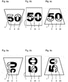
- FIG 8b a development of the security element 1 according to the invention is shown.
- the orientation of the facets 6 is selected in such a way that they each have only a relatively small angle of inclination in the area of the central strip shown in white.
- angles of inclination can be selected from the range of ⁇ 5 °.
- the limits of the area from which the angles of inclination can be selected shift with increasing distance from the center to larger angles of inclination.
- the azimuth angles are each selected from a range such that the mean reflection angle is up in the upper area and down in the lower area.
- the security element 1 is designed as a security thread 19 ( Figure 1 ) there are arrangements in which not only individual at Tilting wandering strips 20 are present, but the effect is continued periodically.
- a security thread 19 that emerges at certain window areas on the surface of the bank note 2 a large number of such effects can be applied to e.g. B. 5 mm repeat periodically.
- the effect can therefore always be perceived at least twice, ie there are always at least two light stripes 20 to be seen.
- the mean inclination in the area of the strip 20 is relatively small in the position of FIG. 9b and increases continuously to the right and left.
- the azimuth angles are selected in such a way that the facets in the left area are oriented upwards, for example, and downwards in the right area, for example.
- the described effect can thus be achieved, the glittering impression again being achieved here due to the random variation in the orientation of the facets of different pixels if only a certain narrow range of variation is given for each area.
- the security element 1 can be arranged on a bank note 2 which also contains a security feature based on preferably platelet-shaped magnetic pigments which are oriented relative to the surface of the bank note in such a way that they form a so-called "rolling bar". Show effect.
- Such alignments can in particular US 7,517,578 B2 can be removed.
- the security element 1 and the magnetic security feature are arranged with respect to one another in such a way that the light stripe of the security element 1 and the light stripe of the magnetic security feature migrate in directions perpendicular to one another when the bank note 2 is tilted.
- the security element according to the invention can be produced in that first the first surface area 3 is computationally divided into the pixels 5. A desired orientation is then calculated for each pixel 5. This can correspond, for example, to the mean expected orientation of a pigment of known security colors. In particular, a grid period or the width of the saw teeth d can be specified.
- the essentially random variation in the orientations of the facets 6 becomes then preferably implemented in such a way that, proceeding from such a preferred orientation, the orientation of the facets 6 of the individual pixels 5 is then varied, for example on the basis of computer-generated random numbers or pseudo-random numbers. It can thus be achieved in particular that the orientations of the facets 6 of individual pixels 5 fluctuate around a predetermined mean orientation.
- the random variations in orientation can take place in one or two dimensions or spatial directions.
- the variation can also relate only to the slope ⁇ or only to the azimuth angle ⁇ , or the variation of the orientations of the facets 6 can be selected so that a reflected light beam incident in a corresponding sub-area fans out around a predetermined direction of rotation.
- the sawtooth structures of the individual pixels 5 can then be generated by means of gray-scale lithography, for example. This structure can then be electroplated and embossed in UV varnish 9 in mass production on foil. The metal film 12 is then vapor-deposited and then the thin-film interference coating 18, if necessary.
- the orientations of the facets 6 of the pixels 5 can be produced with high accuracy, so that a very fine resolution can be achieved on the small length scale of the pixels 5.
- any sharp or soft transitions can be generated by the individual pixels 5.
- the orientation can be established for each facet 6 in the manner described and after this determination the security element 1 can then be produced.
- the security element 1 according to the invention can also be used as a security thread 19 ( Figure 1 ) be trained. Furthermore, the security element 1 can not only as described, are formed on a carrier film from which it can be transferred to the value document in a known manner. It is also possible to form the security element 1 directly on the value document. For example, direct printing with subsequent embossing of the security element on a polymer substrate can be carried out in order to form a security element according to the invention, for example in the case of plastic banknotes.
- the security element according to the invention can be formed in a wide variety of substrates.
- a paper with synthetic fibers ie paper with a proportion of x polymeric material in the range of 0 ⁇ x ⁇ 100% by weight
- a plastic film e.g. B. a film made of polyethylene (PE), polyethylene terephthalate (PET), polybutylene terephthalate (PBT), polyethylene naphthalate (PEN), polypropylene (PP) or polyamide (PA), or a multilayer composite, in particular a composite of several different films (composite) or a paper-film composite (film / paper / film or paper / film / paper), wherein the security element can be provided in or on or between each of the layers of such a multilayer composite.
- PE polyethylene
- PET polyethylene terephthalate
- PBT polybutylene terephthalate
- PEN polyethylene naphthalate
- PA polyamide
- a multilayer composite in particular a composite of several different films (composite) or a paper-film composite (film / paper
- FIG. 10 Another embodiment of the security element 1 according to the invention is shown in plan view, in which the first surface area 3 is again formed by the digits of the number 50 and the second surface area 4 adjoins the first surface area 3 in such a way that both surface areas 3 and 4 together cover the entire area fill in, which is limited by the rectangular outer contour of the optically variable surface pattern 1.
- the first area 3 can be in connection with Figures 1 to 9 described types, so that, for example, the glittering effect according to the invention and / or the described noisy representation is achieved can be.
- Figures 8a-8c Rolling bar effect
- the second surface area 4 is designed here as a moiré magnification arrangement, which will be described in detail below, which represents the letter “M” for the viewer with absolute depth information. This results in an overall representation for the viewer in which the two surface areas 3, 4 or the individual representations presented by the surface areas 3 and 4 result in an overall picture, the two surface areas 3, 4 preferably directly adjoining one another.
- the two surface areas can be combined on the same carrier 9 (which can, for example, be designed as a film strip) and in particular can be embossed in the same work steps.
- FIG. 11 is a schematic sectional view of the security element 1 according to FIG Figure 10 shown, the sectional view showing a portion of the first surface area 3, to which the second surface area 4 adjoins on both sides.
- the sectional view according to Figure 11 is purely schematic and not true to scale and mainly serves to explain the structure.
- the carrier 9 has a carrier film 21 (which can be a PET film, for example) and an upper and lower embossing lacquer layer 22, 23.
- facets 6 of the pixels 5 2 and 5 3 are shown schematically.
- the desired reflection of the individual pixels 5 2 , 5 3 is achieved by means of the facets 6.
- microstructures 24, which can in particular be filled with color, are formed in the lower embossing lacquer layer 23.
- the microstructures 24 are in a plane perpendicular to the plane of the drawing Figure 11 arranged in a grid with a fixed geometry (here, for example, a hexagonal grid) and thus flat in a first microstructure pattern.
- the upper embossing lacquer layer 22 is designed in such a way that it has a multiplicity of microlenses 25 in the second surface area 4.
- the microlenses 25 are in a plane perpendicular to the plane of the drawing Figure 11 Arranged in a grid with a fixed geometry (here, for example, a hexagonal grid) and thus flat in a first pattern, the first pattern being adapted to the first microstructure pattern and both patterns being aligned with one another in such a way that when the security element 1 is viewed, the microlenses 25 come together form a moiré magnification arrangement with the microstructures 24.
- the basic principle of a moiré magnification arrangement is, for example, in WO 2006/087138 A1 the entire content of which is hereby incorporated.
- the moiré magnification arrangement in the second surface part 4 forms a micro-optical display arrangement 26 with which, as will be described in detail below, the letter “M” is repeatedly displayed to the viewer so that it appears behind the security element 1.
- the left and right eyes LA and RA of the viewer are presented with different views of the object to be displayed (here the letter "M"), each of which shows the object viewed from the corresponding direction.
- the object is drawn in as a point to simplify the representation, with the right
- the observer's eye RA sees the object at position 27 and the observer's left eye LA sees the object at position 28.
- the observer thus sees the object with his two eyes in the different directions 29, 30, which intersect at position 31, so that for the observer the object is located at position 31 and therefore at distance t1 behind security element 1. For the observer, this results in absolute depth information for the object.
- the moiré magnification arrangement in the second surface area 4 achieves an absolute depth effect in which the periodically recurring letter "M" located in the depth t1 is displayed for the viewer.
- the microstructures 24 can preferably be filled with color, so that the letters “M” on the one hand and the remaining area of the second surface area 4 on the other hand appear matt but differently colored.
- the micro-optical display arrangement 26 can be designed not only as a moiré magnification arrangement, but also, for example, as a modulo magnification arrangement, as it is, for example, in FIG WO 2009/000528 A1 is described.
- the content relating to the formation of a modulo magnification arrangement of WO 2009/000528 A1 is hereby incorporated into the present application.
- a modulo magnification arrangement in contrast to a moiré magnification arrangement, the image to be displayed does not necessarily have to emerge periodically from a grid assemble repeating individual motifs. A complex single image can be displayed with high resolution.
- the image to be displayed generally consists of individual motifs (here microstructures 24) which are periodically arranged in a grid and which are enlarged by the lenses 25, with the area assigned to each individual motif at most approximately the area of the corresponding lens cell is equivalent to.
- the microlenses 25 and the sawtooth structures for the reflective facets 6 can be produced simultaneously next to one another by means of only a single embossing of the embossing layer 22. Then only the facets 6 need to be metallized so that they have a reflective effect.
- the structure according to Figure 11 is therefore quick to manufacture.
- FIG 13 a modification of the security element 1 according to the invention is shown in which the micro-optical display arrangement 26 has, instead of the microlenses 25, concave mirrors 32 which are formed by embossing the lower embossing lacquer layer 23 and applying a reflective coating.
- the facets 6 of the pixels 5 2 , 5 3 are also formed on the lower embossing lacquer layer 23. They can be formed in the same way as the micro-concave mirror 32 by embossing and mirroring.
- the concave micro mirrors 32 and the facets are preferably embossed in the same step and mirrored in the same step.
- the microstructures 24 can be provided not only in the second surface area 4, but also in the first surface area 3 and thus above the facets 6. This simplifies the production of the security element 1. However, they can also be omitted.
- the first surface area 3 can (but does not have to) also appear slightly colored.
- FIG 14 A structure of the security element 1 is shown in which the micro-concave mirror 32, the microstructures 24 and the facets 6 are each embossed in their own embossing lacquer layer 23, 22 and 33.
- a first carrier film 21 is provided between the embossing lacquer layers 23 and 22 and a second carrier film 34 is provided between the embossing lacquer layers 22 and 33.
- micro-concave mirror 32 and the facets 6 can be metallized differently, for example with different metals or coatings with color-shifting effects (for example thin-film systems in which the color varies depending on the viewing angle).
- a further protective lacquer layer (not shown) can also advantageously be provided on the upper side or lower side of the security element 1, so that the resistance and the protection against impressions by counterfeiters can be increased.
- the micro-optical display arrangement 26 can also only have a perforated grid 35 instead of a microfocusing element grid (grid from the microlenses 25 or grid from the micro-concave mirrors 32), as in FIG Figure 15 is shown.
- a perforated grid 35 can be implemented, for example, by means of periodically arranged holes or slits in an opaque, for example mirror-metallized, layer.
- the holes can be small recesses. In this case, the holes can be called positive holes. So-called negative holes can also be provided, in which the holes are small, non-transparent or non-reflective areas.
- the perforated grid also extends into the first surface area 3, so that the representations are superimposed in the first surface area 3.
- the security element 1 can also be designed in such a way that there is no hole pattern in the first surface area 3.
- the micro-optical display arrangement 26 can be implemented by means of diffractive structures.
- a hologram with a stereographic 3D representation can be provided, which is made up of microscopic sinusoidal gratings.
- the object displayed by means of the micro-optical display arrangement 26 can also appear to lie or float in front of the security element 1.
- the micro-optical display arrangement 26 and / or the facets 6 can be provided entirely or partially with a color-changing coating, in particular a thin film with a reflector / dielectric / absorber. In this way, the visual attractiveness can be further increased and the protection against forgery can be further increased.
- the micro-optical display arrangement 26 in the second surface area 4 was designed in such a way that a stereographic display with depth information is achieved.
- This is understood here to mean representations in which a three-dimensional effect is generated in that the security element 1 provides the left and right eyes of the observer with different views of an object, each of which shows the object viewed from the corresponding direction. From these different views, absolute depth information is then obtained for a viewer, resulting in a three-dimensional impression overall.
- the representations used in this class can often have more than just two different views, which usually results in parallax (i.e. when rotating, the image components in the foreground move relative to the image components in the background). Under certain circumstances, for example, you can look behind an object in the foreground by rotating it.
- holograms for example directly exposed holograms or computer-generated stereograms.
- microlens tilt images and moiré magnification arrangements with a depth effect or a movement effect as is the case, for example, in FIG WO 2007/076952 A2 or WO 2009/000527 A1 is described.
- the micro-optical display arrangement 26 can now be designed in such a way that the parallax does not exactly correspond to the parallax of an object lying in the depth. This can be achieved, for example, by means of moiré magnification arrangements or modulo magnification arrangements. It can thereby be achieved that when the security element 1 is tilted or rotated, an additional movement effect occurs in the second surface area 4. This can be an orthoparallactic movement, as it is, for. B. in the WO 2007/076952 A2 is described, wherein the representations for the left and right eye of the observer do not, strictly speaking, allow an assignment of a depth, since the viewing directions under which the observer sees the object with the left and right eyes do not intersect.
- a representation with correct parallax corresponds to a representation with an A matrix that is only occupied on the diagonal.
- the A-matrix is only occupied in the places that are not on the diagonal. There is a small error in parallax when the A-matrix is occupied both on the diagonal and next to it.
- the display by means of the micro-optical display arrangement 26 can change from a first image to a second image when the security element 1 is tilted or rotated.
- the micro-optical display arrangement 26 can also realize additional effects, for example tilt images or kinematic effects (movements, pumping effect, etc.).
- additional effects for example tilt images or kinematic effects (movements, pumping effect, etc.).
- the three-dimensional representation in the second surface area 4 can move when the security element 1 is tilted.
- the display could also tilt into the display of a completely different object that does not necessarily also appear three-dimensional (for example, a number lying in the depth can change to another display, for example a symbol that then moves when tilted further).
- micro-optical display arrangement 26 and the facets 6 in the same embossing lacquer layer 22 ( Figures 11 and 14th ) so that a micro-optical display arrangement 26 can be upgraded to the security element 1 according to the invention with extremely little effort. It is only necessary to write the facets 6 additionally between or next to the microlenses 25 or micro-concave mirrors 32 during the origination.
- the security element 1 according to the invention can also be referred to as an optically variable surface pattern and z. B. can be used for purely decorative purposes.
- an embossing tool 36 is shown schematically with which the facets 6 and the microlenses 25 in the upper embossing lacquer layer 22 of the security element 1 according to Fig. 11 can be embossed.
- the embossing tool 36 has an embossing surface 37 in which the inverted shape of the surface structure to be embossed is formed.
- embossing tool can also be made available in the same way for the other described embodiments.
Landscapes
- Physics & Mathematics (AREA)
- General Physics & Mathematics (AREA)
- Optics & Photonics (AREA)
- Business, Economics & Management (AREA)
- Accounting & Taxation (AREA)
- Finance (AREA)
- Engineering & Computer Science (AREA)
- Manufacturing & Machinery (AREA)
- Credit Cards Or The Like (AREA)
- Printing Methods (AREA)
Priority Applications (2)
| Application Number | Priority Date | Filing Date | Title |
|---|---|---|---|
| EP25151219.0A EP4512631A3 (fr) | 2009-12-04 | 2010-12-03 | Élément de sécurité, document de valeur doté d'un tel élément de sécurité et procédé de fabrication d'un élément de sécurité |
| EP26152915.0A EP4714668A3 (fr) | 2009-12-04 | 2010-12-03 | Élément de sécurité, document de valeur doté d'un tel élément de sécurité et procédé de fabrication d'un élément de sécurité |
Applications Claiming Priority (5)
| Application Number | Priority Date | Filing Date | Title |
|---|---|---|---|
| DE102009056932 | 2009-12-04 | ||
| DE102010047250A DE102010047250A1 (de) | 2009-12-04 | 2010-10-04 | Sicherheitselement, Wertdokument mit einem solchen Sicherheitselement sowie Herstellungsverfahren eines Sicherheitselementes |
| EP10790524.2A EP2507068B1 (fr) | 2009-12-04 | 2010-12-03 | Élément de sécurité, document de valeur présentant un tel élément de sécurité, et procédé de production d'un élément de sécurité |
| PCT/EP2010/007369 WO2011066991A2 (fr) | 2009-12-04 | 2010-12-03 | Élément de sécurité, document de valeur présentant un tel élément de sécurité, et procédé de production d'un élément de sécurité |
| EP17000520.1A EP3216620B1 (fr) | 2009-12-04 | 2010-12-03 | Élement de securite, document de valeur dote d'un tel element de securite ainsi que procede de fabrication d'un element de securite |
Related Parent Applications (3)
| Application Number | Title | Priority Date | Filing Date |
|---|---|---|---|
| EP10790524.2A Division EP2507068B1 (fr) | 2009-12-04 | 2010-12-03 | Élément de sécurité, document de valeur présentant un tel élément de sécurité, et procédé de production d'un élément de sécurité |
| EP17000520.1A Division-Into EP3216620B1 (fr) | 2009-12-04 | 2010-12-03 | Élement de securite, document de valeur dote d'un tel element de securite ainsi que procede de fabrication d'un element de securite |
| EP17000520.1A Division EP3216620B1 (fr) | 2009-12-04 | 2010-12-03 | Élement de securite, document de valeur dote d'un tel element de securite ainsi que procede de fabrication d'un element de securite |
Related Child Applications (3)
| Application Number | Title | Priority Date | Filing Date |
|---|---|---|---|
| EP26152915.0A Division EP4714668A3 (fr) | 2009-12-04 | 2010-12-03 | Élément de sécurité, document de valeur doté d'un tel élément de sécurité et procédé de fabrication d'un élément de sécurité |
| EP25151219.0A Division-Into EP4512631A3 (fr) | 2009-12-04 | 2010-12-03 | Élément de sécurité, document de valeur doté d'un tel élément de sécurité et procédé de fabrication d'un élément de sécurité |
| EP25151219.0A Division EP4512631A3 (fr) | 2009-12-04 | 2010-12-03 | Élément de sécurité, document de valeur doté d'un tel élément de sécurité et procédé de fabrication d'un élément de sécurité |
Publications (2)
| Publication Number | Publication Date |
|---|---|
| EP3851290A1 true EP3851290A1 (fr) | 2021-07-21 |
| EP3851290B1 EP3851290B1 (fr) | 2025-02-19 |
Family
ID=43972572
Family Applications (5)
| Application Number | Title | Priority Date | Filing Date |
|---|---|---|---|
| EP21020030.9A Active EP3851290B1 (fr) | 2009-12-04 | 2010-12-03 | Élement de sécurité, document de valeur doté d'un tel élément de sécurité, ainsi que procédé de fabrication d'un élément de sécurité |
| EP25151219.0A Pending EP4512631A3 (fr) | 2009-12-04 | 2010-12-03 | Élément de sécurité, document de valeur doté d'un tel élément de sécurité et procédé de fabrication d'un élément de sécurité |
| EP17000520.1A Active EP3216620B1 (fr) | 2009-12-04 | 2010-12-03 | Élement de securite, document de valeur dote d'un tel element de securite ainsi que procede de fabrication d'un element de securite |
| EP10790524.2A Active EP2507068B1 (fr) | 2009-12-04 | 2010-12-03 | Élément de sécurité, document de valeur présentant un tel élément de sécurité, et procédé de production d'un élément de sécurité |
| EP26152915.0A Pending EP4714668A3 (fr) | 2009-12-04 | 2010-12-03 | Élément de sécurité, document de valeur doté d'un tel élément de sécurité et procédé de fabrication d'un élément de sécurité |
Family Applications After (4)
| Application Number | Title | Priority Date | Filing Date |
|---|---|---|---|
| EP25151219.0A Pending EP4512631A3 (fr) | 2009-12-04 | 2010-12-03 | Élément de sécurité, document de valeur doté d'un tel élément de sécurité et procédé de fabrication d'un élément de sécurité |
| EP17000520.1A Active EP3216620B1 (fr) | 2009-12-04 | 2010-12-03 | Élement de securite, document de valeur dote d'un tel element de securite ainsi que procede de fabrication d'un element de securite |
| EP10790524.2A Active EP2507068B1 (fr) | 2009-12-04 | 2010-12-03 | Élément de sécurité, document de valeur présentant un tel élément de sécurité, et procédé de production d'un élément de sécurité |
| EP26152915.0A Pending EP4714668A3 (fr) | 2009-12-04 | 2010-12-03 | Élément de sécurité, document de valeur doté d'un tel élément de sécurité et procédé de fabrication d'un élément de sécurité |
Country Status (10)
| Country | Link |
|---|---|
| US (1) | US9176266B2 (fr) |
| EP (5) | EP3851290B1 (fr) |
| CN (1) | CN102712207B (fr) |
| AU (1) | AU2010327032C1 (fr) |
| BR (1) | BR112012013450B1 (fr) |
| CA (1) | CA2780458C (fr) |
| DE (1) | DE102010047250A1 (fr) |
| PH (1) | PH12012501077A1 (fr) |
| RU (1) | RU2564581C2 (fr) |
| WO (1) | WO2011066991A2 (fr) |
Families Citing this family (119)
| Publication number | Priority date | Publication date | Assignee | Title |
|---|---|---|---|---|
| EP2228234A1 (fr) * | 2007-11-16 | 2010-09-15 | Semco Corporation | Carte d'image, dispositif et procédé de gravure d'image |
| DE102009033221A1 (de) * | 2009-07-14 | 2011-01-27 | Human Bios Gmbh | Sicherheitselement zur Kennzeichnung oder Identifikation von Gegenständen und Lebewesen |
| DE102010019766A1 (de) | 2010-05-07 | 2011-11-10 | Giesecke & Devrient Gmbh | Verfahren zur Erzeugung einer Mikrostruktur auf einem Träger |
| DE102010025775A1 (de) * | 2010-07-01 | 2012-01-05 | Giesecke & Devrient Gmbh | Sicherheitselement sowie Wertdokument mit einem solchen Sicherheitselement |
| DE102011014114B3 (de) | 2011-03-15 | 2012-05-10 | Ovd Kinegram Ag | Mehrschichtkörper und Verfahren zur Herstellung eines Mehrschichtkörpers |
| DE102011112554A1 (de) * | 2011-09-06 | 2013-03-07 | Giesecke & Devrient Gmbh | Verfahren zur Herstellung eines Sicherheitspapiers und Mikrolinsenfaden |
| DE102011119598A1 (de) | 2011-11-29 | 2013-05-29 | Ovd Kinegram Ag | Optisch variables Element |
| DE102011120063A1 (de) | 2011-12-02 | 2013-06-06 | Giesecke & Devrient Gmbh | Sicherheitspapier und daraus erhältliches Wertdokument |
| DE102011120850A1 (de) | 2011-12-09 | 2013-06-13 | Giesecke & Devrient Gmbh | Sicherheitspapier, daraus erhältliches Wertdokument und Verfahren zum Herstellen derselben |
| DE102011121653A1 (de) | 2011-12-19 | 2013-06-20 | Giesecke & Devrient Gmbh | Optisch variables Flächenmuster |
| DE102012004195A1 (de) | 2012-03-01 | 2013-09-05 | Giesecke & Devrient Gmbh | Verfahren zum Herstellen eines Wertdokuments und daraus erhältliches Wertdokument |
| WO2013143089A1 (fr) * | 2012-03-28 | 2013-10-03 | 中钞特种防伪科技有限公司 | Élément d'anti-contrefaçon optique et produit utilisant élément d'anti-contrefaçon optique |
| DE102012006623A1 (de) | 2012-03-30 | 2013-10-02 | Giesecke & Devrient Gmbh | Verfahren zum Herstellen eines Datenträgers und daraus erhältlicher Datenträger |
| GB201208137D0 (en) * | 2012-05-10 | 2012-06-20 | Rue De Int Ltd | Security devices and methods of manufacture therefor |
| MX353329B (es) * | 2012-06-01 | 2018-01-08 | Toppan Printing Co Ltd | Pantalla de reflexion unisometrica, portador de informacion que utiliza la pantalla de reflexion unisometrica. |
| DE102012220392B4 (de) * | 2012-11-08 | 2025-04-24 | Bundesdruckerei Gmbh | Wert- und/oder Sicherheitsprodukt mit einem Schutzelement für einen Halbleiter-Chip |
| CN103832114B (zh) * | 2012-11-27 | 2017-10-24 | 中钞特种防伪科技有限公司 | 一种光学防伪元件及使用该光学防伪元件的产品 |
| CN103847289B (zh) * | 2012-11-29 | 2016-03-23 | 中钞特种防伪科技有限公司 | 具有再现隐藏图像的光学防伪元件及用其制成的产品 |
| CN103087555B (zh) * | 2012-12-11 | 2014-12-03 | 中钞油墨有限公司 | 具有防伪功能的微结构金属颜料及其制备方法 |
| DE102013002137A1 (de) | 2013-02-07 | 2014-08-07 | Giesecke & Devrient Gmbh | Optisch variables Flächenmuster |
| FR3005068B1 (fr) * | 2013-04-26 | 2017-05-26 | Arjowiggins Security | Element de securite comportant un hologramme en volume. |
| CN104223620A (zh) * | 2013-06-20 | 2014-12-24 | 中钞特种防伪科技有限公司 | 一种币章 |
| DE102013016041A1 (de) * | 2013-09-26 | 2015-03-26 | Giesecke & Devrient Gmbh | Sicherheitselement mit Linsenrasterbild |
| DE102013019585A1 (de) | 2013-11-21 | 2015-05-21 | Giesecke & Devrient Gmbh | Verfahren zum Herstellen eines Wertdokuments und eines Sicherheitselements, daraus erhältliches Wertdokument und Sicherheitselement und Vorrichtung zur Durchführung des Verfahrens |
| DE102013019943A1 (de) * | 2013-11-27 | 2015-05-28 | Giesecke & Devrient Gmbh | Sicherheitselement mit magnetisch ausrichtbaren Magnetpigmenten und Verfahren zu dessen Herstellung |
| GB201400910D0 (en) | 2014-01-20 | 2014-03-05 | Rue De Int Ltd | Security elements and methods of their manufacture |
| FR3019496A1 (fr) * | 2014-04-07 | 2015-10-09 | Hologram Ind | Composant optique de securite a effet reflectif, fabrication d'un tel composant et document securise equipe d'un tel composant |
| AT515845B1 (de) * | 2014-06-10 | 2017-05-15 | Hueck Folien Gmbh | Sicherheitselement und Verfahren zur Herstellung eines Sicherheitselements mit lichtstreuenden Strukturen |
| EP3166798B1 (fr) | 2014-07-07 | 2020-08-19 | Security Fibres UK Limited | Améliorations de documents de sécurité |
| CN104237988A (zh) * | 2014-09-04 | 2014-12-24 | 兰州空间技术物理研究所 | 一种高衍射效率闪耀光栅结构 |
| CN104385800B (zh) | 2014-10-16 | 2017-10-24 | 中钞特种防伪科技有限公司 | 光学防伪元件及光学防伪产品 |
| WO2016065331A2 (fr) | 2014-10-24 | 2016-04-28 | Wavefront Technology, Inc. | Produits optiques, gabarits pour la fabrication de produits optiques, et procédés de fabrication de gabarits et de produits optiques |
| EP3220171B1 (fr) * | 2014-11-10 | 2022-04-27 | Toppan Printing Co., Ltd. | Élément optique anti-contrefaçon |
| DE102014018890A1 (de) | 2014-12-17 | 2016-06-23 | Giesecke & Devrient Gmbh | Sicherheitselement, Verfahren zum Herstellen desselben und mit dem Sicherheitselement ausgestatteter Datenträger |
| DE102014019088A1 (de) * | 2014-12-18 | 2016-06-23 | Giesecke & Devrient Gmbh | Optisch variables Durchsichtssicherheitselement |
| DE102015005911A1 (de) * | 2015-05-07 | 2016-11-10 | Giesecke & Devrient Gmbh | Optisch variables Sicherheitselement |
| DE102015005969A1 (de) * | 2015-05-08 | 2016-11-10 | Giesecke & Devrient Gmbh | Optisch variables Sicherheitselement |
| AT517320B1 (de) | 2015-05-29 | 2020-04-15 | Hueck Folien Gmbh | Sicherheitselement mit Farbkippeffekt |
| WO2017011476A1 (fr) | 2015-07-13 | 2017-01-19 | Wavefront Technology, Inc. | Produits optiques, gabarits pour la fabrication de produits optiques, et procédés de fabrication de gabarits et de produits optiques |
| CN107850708B (zh) * | 2015-07-15 | 2022-03-22 | 凸版印刷株式会社 | 显示体 |
| US10281626B2 (en) * | 2015-07-25 | 2019-05-07 | NanoMedia Solutions Inc. | Color image display devices comprising structural color pixels that are selectively activated and/or deactivated by material deposition |
| DE102015009786A1 (de) | 2015-07-27 | 2017-02-02 | Giesecke & Devrient Gmbh | Prägewerkzeug zur Herstellung eines Sicherheitselements mit einer optisch variablen Struktur |
| US20180231697A1 (en) | 2015-08-07 | 2018-08-16 | Rolic Technologies AG | Azimuthally modulated scattering device |
| DE102015010945A1 (de) * | 2015-08-19 | 2017-02-23 | Giesecke & Devrient Gmbh | Wertdokument |
| US10317691B2 (en) | 2015-12-03 | 2019-06-11 | Lumenco, Llc | Arrays of individually oriented micro mirrors providing infinite axis activation imaging for imaging security devices |
| US10189294B2 (en) | 2015-12-03 | 2019-01-29 | Lumenco, Llc | Arrays of individually oriented micro mirrors for use in imaging security devices for currency and brand authentication |
| US11167582B2 (en) | 2016-02-09 | 2021-11-09 | Toppan Printing Co., Ltd. | Optical element and information recording medium for counterfeit prevention |
| MX383837B (es) | 2016-03-30 | 2025-03-14 | Toppan Printing Co Ltd | Elemento optico preventivo de falsificacion y medio de informacion. |
| CA3015684C (fr) | 2016-04-22 | 2025-09-09 | Hueck Folien Gesellschaft M.B.H. | Dispositifs de commutation optique |
| US12589611B2 (en) | 2016-04-22 | 2026-03-31 | Hueck Folien Gesellschaft M.B.H. | Optical switch devices |
| EP3970984A1 (fr) | 2016-07-25 | 2022-03-23 | Toppan Printing Co., Ltd. | Corps d'affichage |
| DE102016009024A1 (de) | 2016-07-25 | 2018-01-25 | Giesecke+Devrient Currency Technology Gmbh | Sicherheitspapier, Sicherheitselement und Wertdokument |
| JPWO2018025999A1 (ja) * | 2016-08-05 | 2019-06-27 | 凸版印刷株式会社 | 表示体 |
| AU2017364824B2 (en) * | 2016-11-28 | 2022-12-01 | Toppan Printing Co., Ltd. | Display element and method of determining authenticity thereof, and printed material |
| JP6879002B2 (ja) | 2017-03-29 | 2021-06-02 | 凸版印刷株式会社 | 表示体 |
| DE102017003281A1 (de) | 2017-04-04 | 2018-10-04 | Giesecke+Devrient Currency Technology Gmbh | Sicherheitselement mit Reliefstruktur und Herstellungsverfahren hierfür |
| DE102017003532A1 (de) | 2017-04-11 | 2018-10-11 | Giesecke+Devrient Currency Technology Gmbh | Sicherheitselement und Herstellungsverfahren hierfür |
| FR3066142B1 (fr) | 2017-05-12 | 2022-03-11 | Ccl Secure Pty Ltd | Dispositif de securite optique et procede de fabrication |
| FR3066954B1 (fr) * | 2017-06-06 | 2019-11-01 | Surys | Composant optique de securite visible en reflexion, fabrication d'un tel composant et document securise equipe d'un tel composant |
| EP3637172B1 (fr) | 2017-06-06 | 2025-09-10 | Toppan Printing Co., Ltd. | Structure optique |
| DE102017006421A1 (de) * | 2017-07-07 | 2019-01-10 | Giesecke+Devrient Currency Technology Gmbh | Optisch variable Sicherheitsanordnung |
| DE102017008918A1 (de) | 2017-09-22 | 2019-03-28 | Giesecke+Devrient Currency Technology Gmbh | Plättchenförmiges Pigment, Druckfarbe, Sicherheitselement und Herstellungsverfahren |
| DE102017009226A1 (de) | 2017-10-04 | 2019-04-04 | Giesecke+Devrient Currency Technology Gmbh | Optisch variables Durchsichtssicherheitselement und Datenträger |
| WO2019070335A1 (fr) | 2017-10-05 | 2019-04-11 | Wavefront Technology, Inc. | Structures optiques fournissant des effets dichroïques |
| US10747985B2 (en) * | 2017-10-06 | 2020-08-18 | Bo Xiao | Nanostructure pixel sensor and method |
| WO2019077419A1 (fr) | 2017-10-20 | 2019-04-25 | Wavefront Technology, Inc. | Dispositifs commutateurs optiques |
| JP7196859B2 (ja) * | 2017-12-18 | 2022-12-27 | 凸版印刷株式会社 | 表示体及び表示体の製造方法 |
| DE102017011916A1 (de) | 2017-12-21 | 2019-06-27 | Giesecke+Devrient Currency Technology Gmbh | Foliensicherheitselement und Herstellungsverfahren |
| GB2572746B (en) | 2018-03-22 | 2021-10-27 | De La Rue Int Ltd | Security elements and method of manufacture thereof |
| GB2572745B (en) * | 2018-03-22 | 2021-06-09 | De La Rue Int Ltd | Security elements and methods of manufacture thereof |
| GB2572552B (en) * | 2018-03-29 | 2020-08-26 | De La Rue Int Ltd | Optical device and method of manufacture thereof |
| DE102018003602A1 (de) | 2018-05-03 | 2019-11-07 | Giesecke+Devrient Currency Technology Gmbh | Retroreflektierende Folie, Folie, Datenträger und Verwendung |
| DE102018003603A1 (de) | 2018-05-03 | 2019-11-07 | Giesecke+Devrient Currency Technology Gmbh | Sicherheitselement, Datenträger und Verwendung |
| CN110450560B (zh) * | 2018-05-08 | 2020-12-25 | 中钞特种防伪科技有限公司 | 光学防伪元件及其制备方法和光学防伪产品 |
| DE102018004062A1 (de) * | 2018-05-18 | 2019-11-21 | Giesecke+Devrient Currency Technology Gmbh | Sicherheitselement mit Mikroreflektoren |
| DE102018005474A1 (de) * | 2018-07-09 | 2020-01-09 | Giesecke+Devrient Currency Technology Gmbh | Optisch variables Sicherheitselement mit reflektivem Flächenbereich |
| CN110857003B (zh) * | 2018-08-23 | 2020-12-25 | 中钞特种防伪科技有限公司 | 光学防伪元件及其设计方法、防伪产品 |
| CN110936750A (zh) * | 2018-09-21 | 2020-03-31 | 中钞特种防伪科技有限公司 | 光学防伪元件及防伪产品 |
| DE102018008041A1 (de) | 2018-10-11 | 2020-04-16 | Giesecke+Devrient Currency Technology Gmbh | Ziffernblatt für eine Uhr |
| DE102018009912A1 (de) * | 2018-12-17 | 2020-06-18 | Giesecke+Devrient Currency Technology Gmbh | Verfahren zum Herstellen eines optisch variablen Sicherheitselements |
| DE102018010078A1 (de) * | 2018-12-20 | 2020-06-25 | Giesecke+Devrient Currency Technology Gmbh | Optisch variables Sicherheitselement |
| PL3899605T3 (pl) | 2018-12-21 | 2024-09-09 | Karmic Sàrl | Rozwiązanie do wyświetlania co najmniej jednego obrazu przejściowego z wykorzystaniem trójwymiarowych mikrostruktur i zastosowania takiego rozwiązania |
| AU2020218988B2 (en) * | 2019-02-07 | 2025-07-03 | Toppan Printing Co., Ltd. | Optical structure and artifact reduction method |
| CA3132715A1 (fr) | 2019-04-04 | 2020-10-08 | Wavefront Technology, Inc. | Structures optiques fournissant des effets dichroiques |
| CA3134512A1 (fr) | 2019-04-19 | 2020-10-22 | Wavefront Technology, Inc. | Dispositifs commutateurs optiques |
| CN111845148B (zh) | 2019-04-24 | 2022-04-05 | 中钞特种防伪科技有限公司 | 光学防伪元件及其制作方法 |
| DE102019003214A1 (de) | 2019-05-07 | 2020-11-12 | Giesecke+Devrient Currency Technology Gmbh | Dekorelement mit Mehrschichtaufbau und Dekoreinrichtung |
| DE102019003945A1 (de) * | 2019-06-06 | 2020-12-10 | Giesecke+Devrient Currency Technology Gmbh | Optisch variables Sicherheitselement mit mehrfarbigem reflektivem Flächenbereich |
| GB2585703B (en) | 2019-07-12 | 2023-02-22 | De La Rue Int Ltd | Security devices and methods of manufacture |
| EP3766702A1 (fr) * | 2019-07-15 | 2021-01-20 | Giesecke+Devrient Currency Technology GmbH | Élément de sécurité et son procédé de fabrication |
| WO2021016028A1 (fr) | 2019-07-19 | 2021-01-28 | Magic Leap, Inc. | Procédé de fabrication de réseaux de diffraction |
| DE102020000030A1 (de) | 2020-01-03 | 2021-07-08 | Giesecke+Devrient Currency Technology Gmbh | Optisch variables Sicherheitselement |
| DE102020000031A1 (de) * | 2020-01-03 | 2021-07-08 | Giesecke+Devrient Currency Technology Gmbh | Optisch variables Sicherheitselement |
| DE102020000027A1 (de) * | 2020-01-03 | 2021-07-08 | Giesecke+Devrient Currency Technology Gmbh | Optisch variables Sicherheitselement |
| DE102020000389A1 (de) | 2020-01-22 | 2021-07-22 | Giesecke+Devrient Currency Technology Gmbh | Darstellungselement für Lichtfleckenbild |
| DE102020000732A1 (de) * | 2020-02-04 | 2021-08-05 | Giesecke+Devrient Currency Technology Gmbh | Optisch variables Sicherheitselement |
| JP7468213B2 (ja) * | 2020-07-17 | 2024-04-16 | Toppanホールディングス株式会社 | カラーシフトデバイス |
| DE102020005912A1 (de) * | 2020-09-28 | 2022-03-31 | Giesecke+Devrient Currency Technology Gmbh | Verfahren zum Herstellen eines optisch variablen Sicherheitselements |
| WO2022077011A1 (fr) * | 2020-10-07 | 2022-04-14 | Wavefront Technology, Inc. | Produits optiques, gabarits pour la fabrication de produits optiques et procédés de fabrication de gabarits et de produits optiques |
| WO2022077012A1 (fr) | 2020-10-07 | 2022-04-14 | Wavefront Technology, Inc. | Produits optiques, maîtres de fabrication de produits optiques, et procédés de fabrication de maîtres et de produits optiques |
| DE102020006902A1 (de) | 2020-11-10 | 2022-05-12 | Giesecke+Devrient Currency Technology Gmbh | Optisch variables Sicherheitselement und Verfahren zum Erzeugen eines optisch variablen Sicherheitselementes |
| DE102021001588A1 (de) * | 2021-03-25 | 2022-09-29 | Giesecke+Devrient Currency Technology Gmbh | Herstellungsverfahren für ein optisch variables Sicherheitselement |
| CN115230364B (zh) * | 2021-04-25 | 2024-03-29 | 中钞特种防伪科技有限公司 | 光学防伪元件及其设计方法、防伪产品、数据载体 |
| CN115230363B (zh) * | 2021-04-25 | 2024-03-29 | 中钞特种防伪科技有限公司 | 光学防伪元件及其设计方法、防伪产品 |
| DE102021002335A1 (de) * | 2021-05-03 | 2022-12-01 | Giesecke+Devrient Currency Technology Gmbh | Optisch variables sicherheitselement und wertdokument mit dem optisch variablen sicherheitselement |
| DE102021002599A1 (de) | 2021-05-18 | 2022-11-24 | Giesecke+Devrient Currency Technology Gmbh | Optisch variables Darstellungselement |
| EP4129709B1 (fr) | 2021-08-04 | 2025-10-01 | Giesecke+Devrient Currency Technology GmbH | Procédé de fabrication d'un produit semi-fini, un produit semi-fini, un élément de sécurité et un document de valeur |
| DE102021004910A1 (de) * | 2021-09-29 | 2023-03-30 | Giesecke+Devrient Currency Technology Gmbh | Darstellungselement mit einem oberhalb und unterhalb des Substrats schwebenden Bild |
| CN116259128B (zh) * | 2021-12-01 | 2026-02-10 | 中钞特种防伪科技有限公司 | 防伪元件和防伪产品 |
| DE102022000212A1 (de) | 2022-01-20 | 2023-07-20 | Giesecke+Devrient Currency Technology Gmbh | Sicherheitsmerkmal für ein Verifikationssystem, System, Verfahren und Computerprogrammprodukt zur Verifikation eines mit dem Sicherheitsmerkmal versehenen Gegenstands und Verfahren zum Herstellen eines Sicherheitsmerkmal |
| DE102022002470A1 (de) | 2022-07-06 | 2024-01-11 | Giesecke+Devrient Currency Technology Gmbh | Optisch variables Flächenmuster, Wertdokument mit optisch variablem Flächenmuster und Verfahren zur Herstellung eines optisch variablen Flächenmusters |
| DE102022002840A1 (de) | 2022-08-04 | 2024-02-15 | Giesecke+Devrient Currency Technology Gmbh | Sicherheitselement für ein Wertdokument mit lumineszierendem Sicherheitsmerkmal und Verfahren zu dessen Herstellung |
| DE102022002839A1 (de) | 2022-08-04 | 2024-02-15 | Giesecke+Devrient Currency Technology Gmbh | Sicherheitselement für ein Wertdokument mit optisch variablem Primärflächenmuster und verstecktem Sekundärflächenmuster und Verfahren zu dessen Herstellung |
| DE102023125662A1 (de) | 2023-09-21 | 2025-03-27 | Giesecke+Devrient Currency Technology Gmbh | Optisch variables Sicherheitselement mit farbkippendem Interferenzschichtelement, Wertgegenstand und Herstellungsverfahren |
| DE102023125600A1 (de) | 2023-09-21 | 2025-03-27 | Giesecke+Devrient Currency Technology Gmbh | Verfahren zum Herstellen eines Sicherheitselementes mit Reliefstruktur und Sicherheitselement mit Reliefstruktur |
| US12623480B2 (en) | 2024-03-14 | 2026-05-12 | Viavi Solutions Inc. | Optical security element |
| DE102024109646A1 (de) | 2024-04-05 | 2025-10-09 | Giesecke+Devrient Currency Technology Gmbh | Optisch variables Darstellungselement |
| WO2025223838A1 (fr) | 2024-04-22 | 2025-10-30 | Giesecke+Devrient Currency Technology Gmbh | Élément de sécurité optiquement variable, article de valeur et procédé de fabrication |
| GB202406668D0 (en) * | 2024-05-10 | 2024-06-26 | Iqs Group A S | Security elements comprising microrelief structures |
Citations (12)
| Publication number | Priority date | Publication date | Assignee | Title |
|---|---|---|---|---|
| EP0227423A2 (fr) | 1985-12-23 | 1987-07-01 | Flex Products, Inc. | Lamelles optiques en film mince, revêtement optique par réplique, revêtements et encres contenant ces lamelles et procédé |
| US4838648A (en) | 1988-05-03 | 1989-06-13 | Optical Coating Laboratory, Inc. | Thin film structure having magnetic and color shifting properties |
| WO1998053999A1 (fr) * | 1997-05-27 | 1998-12-03 | Fryco Limited | Dispositifs a couleur changeante |
| WO2006087138A1 (fr) | 2005-02-18 | 2006-08-24 | Giesecke & Devrient Gmbh | Element de securite et procede de production de cet element |
| DE102005061749A1 (de) * | 2005-12-21 | 2007-07-05 | Giesecke & Devrient Gmbh | Optisch variables Sicherheitselement und Verfahren zu seiner Herstellung |
| WO2007076952A2 (fr) | 2005-12-23 | 2007-07-12 | Giesecke & Devrient Gmbh | Element de securite |
| DE102006016139A1 (de) | 2006-04-06 | 2007-10-18 | Ovd Kinegram Ag | Mehrschichtkörper mit Volumen-Hologramm |
| JP2008080609A (ja) | 2006-09-27 | 2008-04-10 | Toppan Printing Co Ltd | 偽造防止媒体および偽造防止ステッカー |
| WO2009000528A1 (fr) | 2007-06-25 | 2008-12-31 | Giesecke & Devrient Gmbh | Système de représentation |
| WO2009000527A1 (fr) | 2007-06-25 | 2008-12-31 | Giesecke & Devrient Gmbh | Système de représentation |
| US7517578B2 (en) | 2002-07-15 | 2009-04-14 | Jds Uniphase Corporation | Method and apparatus for orienting magnetic flakes |
| CA2708526A1 (fr) * | 2008-04-18 | 2009-10-22 | Toppan Printing Co., Ltd. | Materiau d'etiquetage et article etiquete |
Family Cites Families (69)
| Publication number | Priority date | Publication date | Assignee | Title |
|---|---|---|---|---|
| US4012843A (en) | 1973-04-25 | 1977-03-22 | Hitachi, Ltd. | Concave diffraction grating and a manufacturing method thereof |
| US4184700A (en) | 1975-11-17 | 1980-01-22 | Lgz Landis & Gyr Zug Ag | Documents embossed with optical markings representing genuineness information |
| CH594936A5 (fr) | 1975-11-17 | 1978-01-31 | Landis & Gyr Ag | |
| US4243618A (en) | 1978-10-23 | 1981-01-06 | Avery International Corporation | Method for forming retroreflective sheeting |
| US4892385A (en) | 1981-02-19 | 1990-01-09 | General Electric Company | Sheet-material authenticated item with reflective-diffractive authenticating device |
| JPS57208514A (en) | 1981-06-19 | 1982-12-21 | Toshiba Corp | Manufacture of diffraction grating |
| US4484797A (en) | 1981-07-20 | 1984-11-27 | Rca Corporation | Diffractive subtractive color filter responsive to angle of incidence of polychromatic illuminating light |
| JPS5912403A (ja) | 1982-07-12 | 1984-01-23 | Matsushita Electric Ind Co Ltd | 局所的グレ−テイング作製方法 |
| CH659433A5 (de) | 1982-10-04 | 1987-01-30 | Landis & Gyr Ag | Dokument mit einem beugungsoptischen sicherheitselement. |
| JPS608802A (ja) | 1983-06-29 | 1985-01-17 | Agency Of Ind Science & Technol | ブレ−ズド格子の製造方法 |
| ATE69407T1 (de) | 1988-03-03 | 1991-11-15 | Landis & Gyr Betriebs Ag | Dokument. |
| DE58906429D1 (de) * | 1988-09-30 | 1994-01-27 | Landis & Gyr Business Support | Beugungselement. |
| EP0375833B1 (fr) | 1988-12-12 | 1993-02-10 | Landis & Gyr Technology Innovation AG | Modèle horizontal optiquement variable |
| KR0163018B1 (ko) | 1988-12-19 | 1999-05-01 | 그림 스티븐 길란 | 회절 격자 |
| US5105306A (en) | 1989-01-18 | 1992-04-14 | Ohala John J | Visual effect created by an array of reflective facets with controlled slopes |
| ES2130124T3 (es) | 1989-09-04 | 1999-07-01 | Commw Scient Ind Res Org | Rejilla de difraccion y metodo de fabricacion. |
| US5428479A (en) | 1989-09-04 | 1995-06-27 | Commonwealth Scientific And Industrial Research Organisation | Diffraction grating and method of manufacture |
| DE59005737D1 (de) | 1989-12-01 | 1994-06-23 | Landis & Gyr Business Support | Anordnung zur Verbesserung der Fälschungssicherheit eines Wertdokumentes. |
| CA2060057C (fr) | 1991-01-29 | 1997-12-16 | Susumu Takahashi | Afficheur a reseau de diffraction |
| WO1993018419A1 (fr) | 1992-03-12 | 1993-09-16 | Commonwealth Scientific And Industrial Research Organisation | Reseau de diffraction de securite a effets optiques speciaux |
| EP0704066B1 (fr) | 1993-05-25 | 2001-10-17 | Commonwealth Scientific And Industrial Research Organisation | Dispositif diffracteur a images multiples |
| EP0766103B1 (fr) | 1993-08-06 | 2001-05-23 | Commonwealth Scientific And Industrial Research Organisation | Dispositif diffractif |
| US6088161A (en) | 1993-08-06 | 2000-07-11 | The Commonwealth Of Australia Commonwealth Scientific And Industrial Research Organization | Diffractive device having a surface relief structure which generates two or more diffraction images and includes a series of tracks |
| US5770120A (en) | 1994-12-09 | 1998-06-23 | Olympus Optical Co., Ltd. | Method of manufacturing die and optical element performed by using the die |
| DE19506880A1 (de) | 1995-02-17 | 1996-08-22 | Hertz Inst Heinrich | Verfahren zur Herstellung von optischen Übergitterstrukturen mittels Elektronenstrahllithographie |
| PL177897B1 (pl) | 1995-10-31 | 2000-01-31 | Remigiusz Gajda | Element optycznie zmienny oraz sposób zapisu elementu optycznie zmiennego i urządzenie do zapisu elementu optycznie zmiennego |
| EP0868313B1 (fr) * | 1995-11-28 | 2000-04-19 | OVD Kinegram AG | Modele de surface variable sur le plan optique |
| CN1193299A (zh) * | 1996-02-29 | 1998-09-16 | 厄纳斯特·祝 | 含有可写的透明全息图的仿伪文件 |
| US5814355A (en) | 1996-04-30 | 1998-09-29 | Minnesota Mining And Manufacturing Company | Mold for producing glittering cube-corner retroreflective sheeting |
| US5840405A (en) | 1996-04-30 | 1998-11-24 | Minnesota Mining And Manufacturing Company | Glittering cube-corner retroreflective sheeting |
| US5770124A (en) | 1996-04-30 | 1998-06-23 | Minnesota Mining And Manufacturing Company | Method of making glittering cube-corner retroreflective sheeting |
| GB9623214D0 (en) | 1996-11-07 | 1997-01-08 | Fryco Ltd | Optical images |
| AUPO384796A0 (en) | 1996-11-26 | 1996-12-19 | Commonwealth Scientific And Industrial Research Organisation | Colour image diffractive device |
| AU738289B2 (en) | 1997-12-09 | 2001-09-13 | Commonwealth Scientific And Industrial Research Organisation | A diffractive device with three-dimensional effects |
| GB9813205D0 (en) | 1998-06-18 | 1998-08-19 | Rue De Int Ltd | Methods of providing images on substrates |
| EP1123215A1 (fr) | 1998-09-08 | 2001-08-16 | Commonwealth Scientific And Industrial Research Organisation | Microstructure en trois dimensions |
| US6987590B2 (en) | 2003-09-18 | 2006-01-17 | Jds Uniphase Corporation | Patterned reflective optical structures |
| US7009789B1 (en) | 2000-02-22 | 2006-03-07 | Mems Optical, Inc. | Optical device, system and method |
| AU2001231674C1 (en) | 2000-04-15 | 2006-07-27 | Ovd Kinegram Ag | Pattern |
| WO2002006858A2 (fr) | 2000-07-18 | 2002-01-24 | Optaglio Limited | Diffracteur |
| AUPR483301A0 (en) | 2001-05-08 | 2001-05-31 | Commonwealth Scientific And Industrial Research Organisation | An optical device and methods of manufacture |
| DE10129939B4 (de) | 2001-06-20 | 2006-06-22 | Ovd Kinegram Ag | Optisch variables Flächenmuster |
| US7106516B2 (en) | 2002-02-04 | 2006-09-12 | Applied Films Gmbh & Co. Kg | Material with spectrally selective reflection |
| DE10206357A1 (de) * | 2002-02-14 | 2003-08-28 | Giesecke & Devrient Gmbh | Sicherheitselement und Sicherheitsdokument mit einem solchen Sicherheitselement |
| DE10214330A1 (de) | 2002-03-28 | 2003-10-16 | Giesecke & Devrient Gmbh | Sicherheitselement und Verfahren zu seiner Herstellung |
| DE10243863A1 (de) * | 2002-08-13 | 2004-02-26 | Giesecke & Devrient Gmbh | Datenträger mit einem optisch variablen Element |
| DE10254500B4 (de) | 2002-11-22 | 2006-03-16 | Ovd Kinegram Ag | Optisch variables Element und dessen Verwendung |
| DE10351129B4 (de) * | 2003-11-03 | 2008-12-24 | Ovd Kinegram Ag | Diffraktives Sicherheitselement mit einem Halbtonbild |
| DE10356146A1 (de) * | 2003-12-02 | 2005-06-30 | Giesecke & Devrient Gmbh | Datenträger und Verfahren zu seiner Herstellung |
| DE10361130A1 (de) | 2003-12-22 | 2005-07-28 | Giesecke & Devrient Gmbh | Sicherheitselement mit Beugungsstruktur und Verfahren zu seiner Herstellung |
| EP1580020A1 (fr) * | 2004-03-24 | 2005-09-28 | Kba-Giori S.A. | Plaque d'impression en creux |
| DE102004017094A1 (de) | 2004-04-07 | 2005-11-03 | Leonhard Kurz Gmbh & Co. Kg | Verfahren zur Herstellung eines Kraftfahrzeug-Nummernschildes sowie ein Kraftfahrzeug-Nummernschild |
| CZ2004869A3 (cs) | 2004-08-06 | 2006-03-15 | Optaglio S. R .O. | Zpusob vytvorení trojrozmerného obrazu, difraktivní prvek a zpusob jeho vytvorení |
| US20070246933A1 (en) | 2004-08-12 | 2007-10-25 | Giesecke & Devrient Gmbh | Security Element Comprising a Support |
| EP1658992A1 (fr) | 2004-11-23 | 2006-05-24 | European Central Bank | Méthode de production les caractéristiques tactiles de sécurité sur des documents de sécurité |
| GB0504959D0 (en) | 2005-03-10 | 2005-04-20 | Rue International De La Ltd | Security device based on customised microprism film |
| ES2563755T3 (es) | 2005-05-18 | 2016-03-16 | Visual Physics, Llc | Presentación de imágenes y sistema de seguridad micro-óptico |
| DE102005025095A1 (de) | 2005-06-01 | 2006-12-07 | Giesecke & Devrient Gmbh | Datenträger und Verfahren zu seiner Herstellung |
| DE102005027380B4 (de) | 2005-06-14 | 2009-04-30 | Ovd Kinegram Ag | Sicherheitsdokument |
| DE102006012732A1 (de) | 2006-03-17 | 2007-09-20 | Giesecke & Devrient Gmbh | Gitterbild |
| US8488242B2 (en) | 2006-06-20 | 2013-07-16 | Opsec Security Group, Inc. | Optically variable device with diffraction-based micro-optics, method of creating the same, and article employing the same |
| DE102007039996B4 (de) * | 2007-02-07 | 2020-09-24 | Leonhard Kurz Stiftung & Co. Kg | Sicherheitselement für ein Sicherheitsdokument und Verfahren zu seiner Herstellung |
| DE102007005884B4 (de) | 2007-02-07 | 2022-02-03 | Leonhard Kurz Stiftung & Co. Kg | Sicherheitsdokument |
| DE102007009646A1 (de) * | 2007-02-26 | 2008-08-28 | Giesecke & Devrient Gmbh | Gitterbild |
| DE102008013167A1 (de) | 2008-03-07 | 2009-09-10 | Giesecke & Devrient Gmbh | Sicherheitselement und Verfahren zu seiner Herstellung |
| DE102008046128B4 (de) | 2008-09-05 | 2024-03-07 | Giesecke+Devrient Currency Technology Gmbh | Optisch variables Sicherheitselement mit Mattbereich |
| FR2942811B1 (fr) | 2009-03-04 | 2011-05-06 | Oberthur Technologies | Element de securite pour document-valeur. |
| DE102009056934A1 (de) | 2009-12-04 | 2011-06-09 | Giesecke & Devrient Gmbh | Sicherheitselement, Wertdokument mit einem solchen Sicherheitselement sowie Herstellungsverfahren eines Sicherheitselementes |
| DE102011014114B3 (de) * | 2011-03-15 | 2012-05-10 | Ovd Kinegram Ag | Mehrschichtkörper und Verfahren zur Herstellung eines Mehrschichtkörpers |
-
2010
- 2010-10-04 DE DE102010047250A patent/DE102010047250A1/de active Pending
- 2010-12-03 EP EP21020030.9A patent/EP3851290B1/fr active Active
- 2010-12-03 RU RU2012127689/12A patent/RU2564581C2/ru active
- 2010-12-03 US US13/513,301 patent/US9176266B2/en active Active
- 2010-12-03 CA CA2780458A patent/CA2780458C/fr active Active
- 2010-12-03 EP EP25151219.0A patent/EP4512631A3/fr active Pending
- 2010-12-03 BR BR112012013450-7A patent/BR112012013450B1/pt active IP Right Grant
- 2010-12-03 AU AU2010327032A patent/AU2010327032C1/en active Active
- 2010-12-03 EP EP17000520.1A patent/EP3216620B1/fr active Active
- 2010-12-03 CN CN201080062188.2A patent/CN102712207B/zh active Active
- 2010-12-03 WO PCT/EP2010/007369 patent/WO2011066991A2/fr not_active Ceased
- 2010-12-03 PH PH1/2012/501077A patent/PH12012501077A1/en unknown
- 2010-12-03 EP EP10790524.2A patent/EP2507068B1/fr active Active
- 2010-12-03 EP EP26152915.0A patent/EP4714668A3/fr active Pending
Patent Citations (12)
| Publication number | Priority date | Publication date | Assignee | Title |
|---|---|---|---|---|
| EP0227423A2 (fr) | 1985-12-23 | 1987-07-01 | Flex Products, Inc. | Lamelles optiques en film mince, revêtement optique par réplique, revêtements et encres contenant ces lamelles et procédé |
| US4838648A (en) | 1988-05-03 | 1989-06-13 | Optical Coating Laboratory, Inc. | Thin film structure having magnetic and color shifting properties |
| WO1998053999A1 (fr) * | 1997-05-27 | 1998-12-03 | Fryco Limited | Dispositifs a couleur changeante |
| US7517578B2 (en) | 2002-07-15 | 2009-04-14 | Jds Uniphase Corporation | Method and apparatus for orienting magnetic flakes |
| WO2006087138A1 (fr) | 2005-02-18 | 2006-08-24 | Giesecke & Devrient Gmbh | Element de securite et procede de production de cet element |
| DE102005061749A1 (de) * | 2005-12-21 | 2007-07-05 | Giesecke & Devrient Gmbh | Optisch variables Sicherheitselement und Verfahren zu seiner Herstellung |
| WO2007076952A2 (fr) | 2005-12-23 | 2007-07-12 | Giesecke & Devrient Gmbh | Element de securite |
| DE102006016139A1 (de) | 2006-04-06 | 2007-10-18 | Ovd Kinegram Ag | Mehrschichtkörper mit Volumen-Hologramm |
| JP2008080609A (ja) | 2006-09-27 | 2008-04-10 | Toppan Printing Co Ltd | 偽造防止媒体および偽造防止ステッカー |
| WO2009000528A1 (fr) | 2007-06-25 | 2008-12-31 | Giesecke & Devrient Gmbh | Système de représentation |
| WO2009000527A1 (fr) | 2007-06-25 | 2008-12-31 | Giesecke & Devrient Gmbh | Système de représentation |
| CA2708526A1 (fr) * | 2008-04-18 | 2009-10-22 | Toppan Printing Co., Ltd. | Materiau d'etiquetage et article etiquete |
Also Published As
| Publication number | Publication date |
|---|---|
| US20120319395A1 (en) | 2012-12-20 |
| BR112012013450A2 (pt) | 2016-04-12 |
| EP2507068A2 (fr) | 2012-10-10 |
| EP3216620B1 (fr) | 2021-03-10 |
| CN102712207A (zh) | 2012-10-03 |
| BR112012013450B1 (pt) | 2019-12-17 |
| EP3216620A1 (fr) | 2017-09-13 |
| WO2011066991A3 (fr) | 2011-07-28 |
| AU2010327032B2 (en) | 2014-07-24 |
| EP4714668A3 (fr) | 2026-04-22 |
| WO2011066991A2 (fr) | 2011-06-09 |
| RU2564581C2 (ru) | 2015-10-10 |
| AU2010327032C1 (en) | 2015-12-03 |
| US9176266B2 (en) | 2015-11-03 |
| EP2507068B1 (fr) | 2017-05-17 |
| EP4714668A2 (fr) | 2026-03-25 |
| PH12012501077A1 (en) | 2013-02-04 |
| CA2780458C (fr) | 2017-10-31 |
| CN102712207B (zh) | 2015-06-17 |
| EP3851290B1 (fr) | 2025-02-19 |
| EP4512631A2 (fr) | 2025-02-26 |
| AU2010327032A1 (en) | 2012-06-21 |
| RU2012127689A (ru) | 2014-01-20 |
| DE102010047250A1 (de) | 2011-06-09 |
| CA2780458A1 (fr) | 2011-06-09 |
| EP4512631A3 (fr) | 2025-04-16 |
Similar Documents
| Publication | Publication Date | Title |
|---|---|---|
| EP3216620B1 (fr) | Élement de securite, document de valeur dote d'un tel element de securite ainsi que procede de fabrication d'un element de securite | |
| EP3339048B1 (fr) | Élément de sécurité ayant une zone de surface réfléchissante | |
| EP1853763B2 (fr) | Element de securite et procede de production de cet element | |
| EP1966769B1 (fr) | Elément de sécurité à variation d'aspect et son procédé de fabrication | |
| EP2853411B1 (fr) | Élément de sécurité avec image lenticulaire | |
| EP3401117B1 (fr) | Élément de sécurité ainsi que document de valeur pourvu d'un tel élément de sécurité | |
| EP2451650B2 (fr) | Corps multicouche | |
| EP4234261B1 (fr) | Élément optiquement variable | |
| EP3291997B1 (fr) | Élément de sécurité optiquement variable | |
| EP2934904B1 (fr) | Élément de sécurité avec une image lenticulaire | |
| EP2385902B1 (fr) | Élément de sécurité et papier de sécurité | |
| DE102009056934A1 (de) | Sicherheitselement, Wertdokument mit einem solchen Sicherheitselement sowie Herstellungsverfahren eines Sicherheitselementes | |
| EP1878584A2 (fr) | Corps multicouche à micro-optique | |
| EP3750717B1 (fr) | Procédé de fabrication d'un élément de sécurité ainsi qu'un élément de sécurité | |
| EP3606765B1 (fr) | Elément de sécurité avec structure en relief et son procédé de fabrication | |
| EP3034315B1 (fr) | Élement de securite, son procede de fabrication et support de donnees dote d'un element de securite | |
| EP3184318A1 (fr) | Élément de sécurité optique variable ayant une zone de surface réfléchissante | |
| EP3600903B1 (fr) | Élément de sécurité | |
| EP4384401A1 (fr) | Procédé de production d'un élément de sécurité, élément de sécurité pour un support de données, support de données et feuille de stratification | |
| DE102005063701B4 (de) | Optisch variables Sicherheitselement und Verfahren zu seiner Herstellung | |
| DE102023121166A1 (de) | Optisch variables Durchsichtssicherheitselement, Datenträger und Herstellungsverfahren | |
| DE102005063700B4 (de) | Optisch variables Sicherheitselement und Verfahren zu seiner Herstellung |
Legal Events
| Date | Code | Title | Description |
|---|---|---|---|
| PUAI | Public reference made under article 153(3) epc to a published international application that has entered the european phase |
Free format text: ORIGINAL CODE: 0009012 |
|
| STAA | Information on the status of an ep patent application or granted ep patent |
Free format text: STATUS: THE APPLICATION HAS BEEN PUBLISHED |
|
| AC | Divisional application: reference to earlier application |
Ref document number: 3216620 Country of ref document: EP Kind code of ref document: P Ref document number: 2507068 Country of ref document: EP Kind code of ref document: P |
|
| AK | Designated contracting states |
Kind code of ref document: A1 Designated state(s): AL AT BE BG CH CY CZ DE DK EE ES FI FR GB GR HR HU IE IS IT LI LT LU LV MC MK MT NL NO PL PT RO RS SE SI SK SM TR |
|
| STAA | Information on the status of an ep patent application or granted ep patent |
Free format text: STATUS: REQUEST FOR EXAMINATION WAS MADE |
|
| 17P | Request for examination filed |
Effective date: 20220121 |
|
| RBV | Designated contracting states (corrected) |
Designated state(s): AL AT BE BG CH CY CZ DE DK EE ES FI FR GB GR HR HU IE IS IT LI LT LU LV MC MK MT NL NO PL PT RO RS SE SI SK SM TR |
|
| STAA | Information on the status of an ep patent application or granted ep patent |
Free format text: STATUS: EXAMINATION IS IN PROGRESS |
|
| 17Q | First examination report despatched |
Effective date: 20220906 |
|
| RAP3 | Party data changed (applicant data changed or rights of an application transferred) |
Owner name: GIESECKE+DEVRIENT CURRENCY TECHNOLOGY GMBH |
|
| P01 | Opt-out of the competence of the unified patent court (upc) registered |
Effective date: 20230519 |
|
| GRAP | Despatch of communication of intention to grant a patent |
Free format text: ORIGINAL CODE: EPIDOSNIGR1 |
|
| STAA | Information on the status of an ep patent application or granted ep patent |
Free format text: STATUS: GRANT OF PATENT IS INTENDED |
|
| INTG | Intention to grant announced |
Effective date: 20240522 |
|
| GRAJ | Information related to disapproval of communication of intention to grant by the applicant or resumption of examination proceedings by the epo deleted |
Free format text: ORIGINAL CODE: EPIDOSDIGR1 |
|
| STAA | Information on the status of an ep patent application or granted ep patent |
Free format text: STATUS: EXAMINATION IS IN PROGRESS |
|
| GRAP | Despatch of communication of intention to grant a patent |
Free format text: ORIGINAL CODE: EPIDOSNIGR1 |
|
| STAA | Information on the status of an ep patent application or granted ep patent |
Free format text: STATUS: GRANT OF PATENT IS INTENDED |
|
| GRAJ | Information related to disapproval of communication of intention to grant by the applicant or resumption of examination proceedings by the epo deleted |
Free format text: ORIGINAL CODE: EPIDOSDIGR1 |
|
| STAA | Information on the status of an ep patent application or granted ep patent |
Free format text: STATUS: EXAMINATION IS IN PROGRESS |
|
| INTC | Intention to grant announced (deleted) | ||
| GRAP | Despatch of communication of intention to grant a patent |
Free format text: ORIGINAL CODE: EPIDOSNIGR1 |
|
| STAA | Information on the status of an ep patent application or granted ep patent |
Free format text: STATUS: GRANT OF PATENT IS INTENDED |
|
| INTG | Intention to grant announced |
Effective date: 20240816 |
|
| INTC | Intention to grant announced (deleted) | ||
| INTG | Intention to grant announced |
Effective date: 20240913 |
|
| GRAS | Grant fee paid |
Free format text: ORIGINAL CODE: EPIDOSNIGR3 |
|
| GRAA | (expected) grant |
Free format text: ORIGINAL CODE: 0009210 |
|
| STAA | Information on the status of an ep patent application or granted ep patent |
Free format text: STATUS: THE PATENT HAS BEEN GRANTED |
|
| AC | Divisional application: reference to earlier application |
Ref document number: 2507068 Country of ref document: EP Kind code of ref document: P Ref document number: 3216620 Country of ref document: EP Kind code of ref document: P |
|
| AK | Designated contracting states |
Kind code of ref document: B1 Designated state(s): AL AT BE BG CH CY CZ DE DK EE ES FI FR GB GR HR HU IE IS IT LI LT LU LV MC MK MT NL NO PL PT RO RS SE SI SK SM TR |
|
| REG | Reference to a national code |
Ref country code: GB Ref legal event code: FG4D Free format text: NOT ENGLISH |
|
| REG | Reference to a national code |
Ref country code: CH Ref legal event code: EP |
|
| REG | Reference to a national code |
Ref country code: DE Ref legal event code: R096 Ref document number: 502010017108 Country of ref document: DE |
|
| REG | Reference to a national code |
Ref country code: IE Ref legal event code: FG4D Free format text: LANGUAGE OF EP DOCUMENT: GERMAN |
|
| REG | Reference to a national code |
Ref country code: NL Ref legal event code: MP Effective date: 20250219 |
|
| PG25 | Lapsed in a contracting state [announced via postgrant information from national office to epo] |
Ref country code: RS Free format text: LAPSE BECAUSE OF FAILURE TO SUBMIT A TRANSLATION OF THE DESCRIPTION OR TO PAY THE FEE WITHIN THE PRESCRIBED TIME-LIMIT Effective date: 20250519 |
|
| PG25 | Lapsed in a contracting state [announced via postgrant information from national office to epo] |
Ref country code: FI Free format text: LAPSE BECAUSE OF FAILURE TO SUBMIT A TRANSLATION OF THE DESCRIPTION OR TO PAY THE FEE WITHIN THE PRESCRIBED TIME-LIMIT Effective date: 20250219 |
|
| PG25 | Lapsed in a contracting state [announced via postgrant information from national office to epo] |
Ref country code: PL Free format text: LAPSE BECAUSE OF FAILURE TO SUBMIT A TRANSLATION OF THE DESCRIPTION OR TO PAY THE FEE WITHIN THE PRESCRIBED TIME-LIMIT Effective date: 20250219 |
|
| PG25 | Lapsed in a contracting state [announced via postgrant information from national office to epo] |
Ref country code: ES Free format text: LAPSE BECAUSE OF FAILURE TO SUBMIT A TRANSLATION OF THE DESCRIPTION OR TO PAY THE FEE WITHIN THE PRESCRIBED TIME-LIMIT Effective date: 20250219 |
|
| REG | Reference to a national code |
Ref country code: LT Ref legal event code: MG9D |
|
| PG25 | Lapsed in a contracting state [announced via postgrant information from national office to epo] |
Ref country code: IS Free format text: LAPSE BECAUSE OF FAILURE TO SUBMIT A TRANSLATION OF THE DESCRIPTION OR TO PAY THE FEE WITHIN THE PRESCRIBED TIME-LIMIT Effective date: 20250619 Ref country code: NO Free format text: LAPSE BECAUSE OF FAILURE TO SUBMIT A TRANSLATION OF THE DESCRIPTION OR TO PAY THE FEE WITHIN THE PRESCRIBED TIME-LIMIT Effective date: 20250519 |
|
| PG25 | Lapsed in a contracting state [announced via postgrant information from national office to epo] |
Ref country code: NL Free format text: LAPSE BECAUSE OF FAILURE TO SUBMIT A TRANSLATION OF THE DESCRIPTION OR TO PAY THE FEE WITHIN THE PRESCRIBED TIME-LIMIT Effective date: 20250219 |
|
| PG25 | Lapsed in a contracting state [announced via postgrant information from national office to epo] |
Ref country code: HR Free format text: LAPSE BECAUSE OF FAILURE TO SUBMIT A TRANSLATION OF THE DESCRIPTION OR TO PAY THE FEE WITHIN THE PRESCRIBED TIME-LIMIT Effective date: 20250219 |
|
| PG25 | Lapsed in a contracting state [announced via postgrant information from national office to epo] |
Ref country code: PT Free format text: LAPSE BECAUSE OF FAILURE TO SUBMIT A TRANSLATION OF THE DESCRIPTION OR TO PAY THE FEE WITHIN THE PRESCRIBED TIME-LIMIT Effective date: 20250620 Ref country code: LV Free format text: LAPSE BECAUSE OF FAILURE TO SUBMIT A TRANSLATION OF THE DESCRIPTION OR TO PAY THE FEE WITHIN THE PRESCRIBED TIME-LIMIT Effective date: 20250219 |
|
| PG25 | Lapsed in a contracting state [announced via postgrant information from national office to epo] |
Ref country code: BG Free format text: LAPSE BECAUSE OF FAILURE TO SUBMIT A TRANSLATION OF THE DESCRIPTION OR TO PAY THE FEE WITHIN THE PRESCRIBED TIME-LIMIT Effective date: 20250219 Ref country code: GR Free format text: LAPSE BECAUSE OF FAILURE TO SUBMIT A TRANSLATION OF THE DESCRIPTION OR TO PAY THE FEE WITHIN THE PRESCRIBED TIME-LIMIT Effective date: 20250520 |
|
| PG25 | Lapsed in a contracting state [announced via postgrant information from national office to epo] |
Ref country code: SE Free format text: LAPSE BECAUSE OF FAILURE TO SUBMIT A TRANSLATION OF THE DESCRIPTION OR TO PAY THE FEE WITHIN THE PRESCRIBED TIME-LIMIT Effective date: 20250219 |
|
| PG25 | Lapsed in a contracting state [announced via postgrant information from national office to epo] |
Ref country code: SM Free format text: LAPSE BECAUSE OF FAILURE TO SUBMIT A TRANSLATION OF THE DESCRIPTION OR TO PAY THE FEE WITHIN THE PRESCRIBED TIME-LIMIT Effective date: 20250219 |
|
| PG25 | Lapsed in a contracting state [announced via postgrant information from national office to epo] |
Ref country code: DK Free format text: LAPSE BECAUSE OF FAILURE TO SUBMIT A TRANSLATION OF THE DESCRIPTION OR TO PAY THE FEE WITHIN THE PRESCRIBED TIME-LIMIT Effective date: 20250219 |
|
| PG25 | Lapsed in a contracting state [announced via postgrant information from national office to epo] |
Ref country code: IT Free format text: LAPSE BECAUSE OF FAILURE TO SUBMIT A TRANSLATION OF THE DESCRIPTION OR TO PAY THE FEE WITHIN THE PRESCRIBED TIME-LIMIT Effective date: 20250219 |
|
| PG25 | Lapsed in a contracting state [announced via postgrant information from national office to epo] |
Ref country code: EE Free format text: LAPSE BECAUSE OF FAILURE TO SUBMIT A TRANSLATION OF THE DESCRIPTION OR TO PAY THE FEE WITHIN THE PRESCRIBED TIME-LIMIT Effective date: 20250219 Ref country code: CZ Free format text: LAPSE BECAUSE OF FAILURE TO SUBMIT A TRANSLATION OF THE DESCRIPTION OR TO PAY THE FEE WITHIN THE PRESCRIBED TIME-LIMIT Effective date: 20250219 |
|
| PG25 | Lapsed in a contracting state [announced via postgrant information from national office to epo] |
Ref country code: RO Free format text: LAPSE BECAUSE OF FAILURE TO SUBMIT A TRANSLATION OF THE DESCRIPTION OR TO PAY THE FEE WITHIN THE PRESCRIBED TIME-LIMIT Effective date: 20250219 |
|
| PG25 | Lapsed in a contracting state [announced via postgrant information from national office to epo] |
Ref country code: SK Free format text: LAPSE BECAUSE OF FAILURE TO SUBMIT A TRANSLATION OF THE DESCRIPTION OR TO PAY THE FEE WITHIN THE PRESCRIBED TIME-LIMIT Effective date: 20250219 |
|
| REG | Reference to a national code |
Ref country code: DE Ref legal event code: R097 Ref document number: 502010017108 Country of ref document: DE |
|
| PLBE | No opposition filed within time limit |
Free format text: ORIGINAL CODE: 0009261 |
|
| STAA | Information on the status of an ep patent application or granted ep patent |
Free format text: STATUS: NO OPPOSITION FILED WITHIN TIME LIMIT |
|
| PGFP | Annual fee paid to national office [announced via postgrant information from national office to epo] |
Ref country code: GB Payment date: 20251218 Year of fee payment: 16 |
|
| PGFP | Annual fee paid to national office [announced via postgrant information from national office to epo] |
Ref country code: AT Payment date: 20251215 Year of fee payment: 16 |
|
| PGFP | Annual fee paid to national office [announced via postgrant information from national office to epo] |
Ref country code: FR Payment date: 20251218 Year of fee payment: 16 |
|
| 26N | No opposition filed |
Effective date: 20251120 |
|
| PGFP | Annual fee paid to national office [announced via postgrant information from national office to epo] |
Ref country code: DE Payment date: 20251222 Year of fee payment: 16 |