EP3863113B1 - Erdungsstruktur für eine hochfrequenz-leiterplatte - Google Patents
Erdungsstruktur für eine hochfrequenz-leiterplatte Download PDFInfo
- Publication number
- EP3863113B1 EP3863113B1 EP19853252.5A EP19853252A EP3863113B1 EP 3863113 B1 EP3863113 B1 EP 3863113B1 EP 19853252 A EP19853252 A EP 19853252A EP 3863113 B1 EP3863113 B1 EP 3863113B1
- Authority
- EP
- European Patent Office
- Prior art keywords
- high frequency
- circuit board
- hole
- frequency circuit
- conductor layer
- Prior art date
- Legal status (The legal status is an assumption and is not a legal conclusion. Google has not performed a legal analysis and makes no representation as to the accuracy of the status listed.)
- Active
Links
Images


Classifications
-
- H—ELECTRICITY
- H05—ELECTRIC TECHNIQUES NOT OTHERWISE PROVIDED FOR
- H05K—PRINTED CIRCUITS; CASINGS OR CONSTRUCTIONAL DETAILS OF ELECTRIC APPARATUS; MANUFACTURE OF ASSEMBLAGES OF ELECTRICAL COMPONENTS
- H05K1/00—Printed circuits
- H05K1/02—Details
- H05K1/0213—Electrical arrangements not otherwise provided for
- H05K1/0237—High frequency adaptations
-
- H—ELECTRICITY
- H01—ELECTRIC ELEMENTS
- H01P—WAVEGUIDES; RESONATORS, LINES, OR OTHER DEVICES OF THE WAVEGUIDE TYPE
- H01P5/00—Coupling devices of the waveguide type
- H01P5/02—Coupling devices of the waveguide type with invariable factor of coupling
- H01P5/022—Transitions between lines of the same kind and shape, but with different dimensions
- H01P5/028—Transitions between lines of the same kind and shape, but with different dimensions between strip lines
-
- H—ELECTRICITY
- H01—ELECTRIC ELEMENTS
- H01P—WAVEGUIDES; RESONATORS, LINES, OR OTHER DEVICES OF THE WAVEGUIDE TYPE
- H01P3/00—Waveguides; Transmission lines of the waveguide type
- H01P3/003—Coplanar lines
- H01P3/006—Conductor backed coplanar waveguides
-
- H—ELECTRICITY
- H01—ELECTRIC ELEMENTS
- H01P—WAVEGUIDES; RESONATORS, LINES, OR OTHER DEVICES OF THE WAVEGUIDE TYPE
- H01P3/00—Waveguides; Transmission lines of the waveguide type
- H01P3/02—Waveguides; Transmission lines of the waveguide type with two longitudinal conductors
- H01P3/08—Microstrips; Strip lines
- H01P3/081—Microstriplines
-
- H—ELECTRICITY
- H05—ELECTRIC TECHNIQUES NOT OTHERWISE PROVIDED FOR
- H05K—PRINTED CIRCUITS; CASINGS OR CONSTRUCTIONAL DETAILS OF ELECTRIC APPARATUS; MANUFACTURE OF ASSEMBLAGES OF ELECTRICAL COMPONENTS
- H05K1/00—Printed circuits
- H05K1/02—Details
- H05K1/0213—Electrical arrangements not otherwise provided for
- H05K1/0237—High frequency adaptations
- H05K1/0243—Printed circuits associated with mounted high frequency components
-
- H—ELECTRICITY
- H05—ELECTRIC TECHNIQUES NOT OTHERWISE PROVIDED FOR
- H05K—PRINTED CIRCUITS; CASINGS OR CONSTRUCTIONAL DETAILS OF ELECTRIC APPARATUS; MANUFACTURE OF ASSEMBLAGES OF ELECTRICAL COMPONENTS
- H05K1/00—Printed circuits
- H05K1/02—Details
- H05K1/0213—Electrical arrangements not otherwise provided for
- H05K1/0237—High frequency adaptations
- H05K1/0246—Termination of transmission lines
-
- H—ELECTRICITY
- H05—ELECTRIC TECHNIQUES NOT OTHERWISE PROVIDED FOR
- H05K—PRINTED CIRCUITS; CASINGS OR CONSTRUCTIONAL DETAILS OF ELECTRIC APPARATUS; MANUFACTURE OF ASSEMBLAGES OF ELECTRICAL COMPONENTS
- H05K1/00—Printed circuits
- H05K1/02—Details
- H05K1/0213—Electrical arrangements not otherwise provided for
- H05K1/0237—High frequency adaptations
- H05K1/025—Impedance arrangements, e.g. impedance matching, reduction of parasitic impedance
- H05K1/0251—Impedance arrangements, e.g. impedance matching, reduction of parasitic impedance related to vias or transitions between vias and transmission lines
-
- H—ELECTRICITY
- H05—ELECTRIC TECHNIQUES NOT OTHERWISE PROVIDED FOR
- H05K—PRINTED CIRCUITS; CASINGS OR CONSTRUCTIONAL DETAILS OF ELECTRIC APPARATUS; MANUFACTURE OF ASSEMBLAGES OF ELECTRICAL COMPONENTS
- H05K1/00—Printed circuits
- H05K1/02—Details
- H05K1/0213—Electrical arrangements not otherwise provided for
- H05K1/0237—High frequency adaptations
- H05K1/025—Impedance arrangements, e.g. impedance matching, reduction of parasitic impedance
- H05K1/0253—Impedance adaptations of transmission lines by special lay-out of power planes, e.g. providing openings
-
- H—ELECTRICITY
- H05—ELECTRIC TECHNIQUES NOT OTHERWISE PROVIDED FOR
- H05K—PRINTED CIRCUITS; CASINGS OR CONSTRUCTIONAL DETAILS OF ELECTRIC APPARATUS; MANUFACTURE OF ASSEMBLAGES OF ELECTRICAL COMPONENTS
- H05K1/00—Printed circuits
- H05K1/02—Details
- H05K1/11—Printed elements for providing electric connections to or between printed circuits
- H05K1/115—Via connections; Lands around holes or via connections
-
- H—ELECTRICITY
- H10—SEMICONDUCTOR DEVICES; ELECTRIC SOLID-STATE DEVICES NOT OTHERWISE PROVIDED FOR
- H10W—GENERIC PACKAGES, INTERCONNECTIONS, CONNECTORS OR OTHER CONSTRUCTIONAL DETAILS OF DEVICES COVERED BY CLASS H10
- H10W44/00—Electrical arrangements for controlling or matching impedance
- H10W44/20—Electrical arrangements for controlling or matching impedance at high-frequency [HF] or radio frequency [RF]
-
- H—ELECTRICITY
- H10—SEMICONDUCTOR DEVICES; ELECTRIC SOLID-STATE DEVICES NOT OTHERWISE PROVIDED FOR
- H10W—GENERIC PACKAGES, INTERCONNECTIONS, CONNECTORS OR OTHER CONSTRUCTIONAL DETAILS OF DEVICES COVERED BY CLASS H10
- H10W70/00—Package substrates; Interposers; Redistribution layers [RDL]
- H10W70/60—Insulating or insulated package substrates; Interposers; Redistribution layers
- H10W70/62—Insulating or insulated package substrates; Interposers; Redistribution layers characterised by their interconnections
- H10W70/65—Shapes or dispositions of interconnections
-
- H—ELECTRICITY
- H05—ELECTRIC TECHNIQUES NOT OTHERWISE PROVIDED FOR
- H05K—PRINTED CIRCUITS; CASINGS OR CONSTRUCTIONAL DETAILS OF ELECTRIC APPARATUS; MANUFACTURE OF ASSEMBLAGES OF ELECTRICAL COMPONENTS
- H05K2201/00—Indexing scheme relating to printed circuits covered by H05K1/00
- H05K2201/09—Shape and layout
- H05K2201/09009—Substrate related
- H05K2201/09036—Recesses or grooves in insulating substrate
-
- H—ELECTRICITY
- H10—SEMICONDUCTOR DEVICES; ELECTRIC SOLID-STATE DEVICES NOT OTHERWISE PROVIDED FOR
- H10W—GENERIC PACKAGES, INTERCONNECTIONS, CONNECTORS OR OTHER CONSTRUCTIONAL DETAILS OF DEVICES COVERED BY CLASS H10
- H10W44/00—Electrical arrangements for controlling or matching impedance
- H10W44/20—Electrical arrangements for controlling or matching impedance at high-frequency [HF] or radio frequency [RF]
- H10W44/251—Electrical arrangements for controlling or matching impedance at high-frequency [HF] or radio frequency [RF] for monolithic microwave integrated circuits [MMIC]
-
- H—ELECTRICITY
- H10—SEMICONDUCTOR DEVICES; ELECTRIC SOLID-STATE DEVICES NOT OTHERWISE PROVIDED FOR
- H10W—GENERIC PACKAGES, INTERCONNECTIONS, CONNECTORS OR OTHER CONSTRUCTIONAL DETAILS OF DEVICES COVERED BY CLASS H10
- H10W90/00—Package configurations
- H10W90/701—Package configurations characterised by the relative positions of pads or connectors relative to package parts
- H10W90/721—Package configurations characterised by the relative positions of pads or connectors relative to package parts of bump connectors
- H10W90/724—Package configurations characterised by the relative positions of pads or connectors relative to package parts of bump connectors between a chip and a stacked insulating package substrate, interposer or RDL
Definitions
- Embodiments of the invention relates to a grounding structure of high frequency circuit board.
- a MMIC (Monolithic Microwave Integrated Circuit) chip often is contained in a surface-mount package such as a QFN (Quad Flat Non-leaded Package).
- This package can be surface-mounted to a high frequency circuit board by using reflow soldering. In such a case, it is desirable to increase the dielectric thickness to reduce the warp of the high frequency circuit board.
- the high frequency characteristics degrade due to an increase of the ground inductance if the grounding is performed via a through-hole provided in a thick dielectric substrate.
- Patent Literature 1 a microwave integrated circuit is disclosed.
- Patent Literature 2 a surface mountable microwave IC package is disclosed.
- Patent Literature 3 a hybrid integrated circuit comprising a dielectric substrate with a through-hole is disclosed.
- a grounding structure of a high frequency circuit board of an embodiment includes a dielectric substrate, a back surface ground electrode, an upper ground electrode, and a microstripline upper electrode.
- the dielectric substrate has a first surface, a second surface provided at a side opposite to the first surface, and a first through-hole provided in the dielectric substrate. A first opening of the first through-hole at the first surface is smaller than a second opening of the first through-hole at the second surface.
- the first grounding conductor layer is provided in the first through-hole.
- the back surface ground electrode is provided at the second surface and connected with the first grounding conductor layer.
- the upper ground electrode is provided at the first surface and connected with at least the first grounding conductor layer.
- the microstripline upper electrode is provided at the first surface.
- the microstripline upper electrode includes at least a first region having a first line width; the microstripline upper electrode has one end portion provided to oppose the first opening and overlap the second opening; and a second line width of the one end portion is narrower than the first line width.
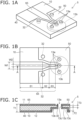
- FIG. 1A is a schematic perspective view of a grounding structure of a high frequency circuit board according to a first embodiment
- FIG. 1B is a schematic top view of the grounding structure
- FIG. 1C is a schematic cross-sectional view along line A-A.
- the grounding structure of the high frequency circuit board 5 includes a dielectric substrate 10, a first grounding conductor layer 30, a back surface ground electrode 40, an upper ground electrode 50, and a microstripline upper electrode 65.
- the dielectric substrate 10 has a first surface 11, and a second surface 12 provided at a side opposite to the first surface 11.
- a first through-hole 13 is provided in the dielectric substrate 10.
- a first opening 13a of the first through-hole 13 at the first surface 11 is smaller than a second opening 13b of the first through-hole 13 at the second surface 12.
- the thickness T1 of the dielectric substrate 10 is set to 0.4 mm, etc.
- the dielectric substrate 10 of the first embodiment has a cross section such as that of FIG. 1C .
- the dielectric substrate 10 is machined from the second surface 12 side.
- the diameter of the second opening 13b is set to 1.7 mm, etc.; and the diameter of the first opening 13a is set to 0.4 mm, etc.
- a depth T2 of the second opening 13b from the second surface 12 is set to 0.3 mm, etc.
- a depth T3 of the first opening 13a from the first surface 11 is set to 0.1 mm, etc.
- the machined surface is metalized.
- the first opening 13a includes three regions.
- the first grounding conductor layer 30 is provided at a sidewall 13c of the first through-hole 13.
- the back surface ground electrode 40 is provided at the second surface 12 and connected with the first grounding conductor layer 30.
- the upper ground electrode 50 is provided at the first surface 11 and connected with the first grounding conductor layer 30.
- the microstripline upper electrode 65 is provided at the first surface 11.
- the microstripline upper electrode 65 includes at least a first region 61. In the drawing, a second region 63 is further provided.
- One end portion of the microstripline upper electrode 65 (in the drawing, the end portion of the second region) is provided to oppose the first opening 13a and overlap the second opening 13b when viewed in plan.
- a line width W2 of the one end portion is narrower than a line width W1 of the first region 61.
- the microstripline upper electrode 65 may include a third region 62 which is provided between the first region 61 and the second region 63, and of which the line width changes continuously.
- FIG. 2A is a schematic plan view of the high frequency circuit board to which a QFN (Quad Flat Non-leaded Package) including a MMIC is mounted using the grounding structure according to the first embodiment; and FIG. 2B is a schematic cross-sectional view along line B-B.
- QFN Quad Flat Non-leaded Package
- a microstripline upper electrode 65a for inputting a signal to the QFN is provided; and a microstripline upper electrode 65b for outputting a signal from the QFN is provided. Also, the two grounding structures are provided respectively at the input terminal side and the output terminal side of the QFN.
- FIG. 3A is a schematic bottom view of the QFN; FIG. 3B is a schematic side view; and FIG. 3C is a schematic top view.
- a pitch P1 between the RF signal input electrode 91 and the ground electrodes (GND) at two sides of the RF signal input electrode 91 is set to 0.5 mm, etc.
- an electrode pattern or the like may not be provided at the upper surface.
- FIG. 4A is a schematic plan view of the QFN surface-mounted to the high frequency circuit board according to the first embodiment; and FIG. 4B is a schematic cross-sectional view along line B-B.
- a high frequency device 90 is surface-mounted to the high frequency circuit board 7 by a reflow soldering process, etc.
- the ground electrode 95 which is provided at the center is connected to the upper ground electrode 50 of the high frequency circuit board 7.
- the high frequency device 90 can be an amplifier, an RF switch, a phase shifter, an attenuator, etc.
- Applications of the high frequency device 90 include millimeter-wave wireless devices, small satellite communication stations, etc.
- the line width W1 of the first region 61 can be set to 0.8 mm; and a width W2 of the second region 63 can be set to 0.25 mm, etc. Therefore, the signal terminal and the ground electrodes next to the signal terminal are not shorted by the microstripline upper electrode 65.
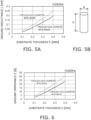
- the reduction of the ground inductance of the first grounding conductor layer 30 provided at the sidewall of the first through-hole 13 and the improvement of the high frequency characteristics at several GHz or more will now be described.
- FIG. 5A is a graph illustrating the ground inductance of the through-hole with respect to the thickness of the dielectric substrate; and FIG. 5B is a schematic perspective view of an example of the through-hole.
- the through-hole has a circular columnar configuration in which the diameter is taken as d , and the height is taken as h .
- the diameter d is 0.2 mm
- the inductance is 0.25 nH when the dielectric substrate thickness is 0.4 mm.
- the inductance is small and is 0.04 nH when the dielectric substrate thickness is 0.1 mm.
- FIG. 6 is a graph illustrating the ground impedance of the through-hole with respect to the dielectric substrate thickness.
- the impedance (@ 20 GHz) due to the ground inductance is about 30 ⁇ .
- impedance (@ 20 GHz) due to the ground inductance is reduced to about 5 ⁇ .
- FIG. 7A is a schematic plan view in which a terminating resistance of 50 S2 is connected between the ground and the microstripline upper electrode of the high frequency circuit board; and FIG. 7B is a graph illustrating the frequency characteristics of the voltage standing wave ratio from an electromagnetic field simulation.
- a terminating resistance R1 is provided between the microstripline upper electrode 65 and the upper ground electrode 50.
- the vertical axis is the VSWR (Voltage Standing Wave Ratio) determined by the electromagnetic field simulation; and the horizontal axis is the frequency.
- VSWR Voltage Standing Wave Ratio
- the horizontal axis is the frequency.
- FIG. 8A is a schematic perspective view of a grounding structure of a high frequency circuit board according to a first comparative example
- FIG. 8B is a schematic plan view of the grounding structure
- FIG. 8C is a schematic cross-sectional view along line D-D.
- the grounding structure of the high frequency circuit board 107 includes a dielectric substrate 110, a first grounding conductor layer 130, a back surface ground electrode 140, an upper ground electrode 150, and a microstripline upper electrode 165.
- a first through-hole 113 is provided in the dielectric substrate 110.
- a thickness T11 of the dielectric substrate 110 can be set to 0.4 mm, etc.
- the back surface ground electrode 140 is connected with the first grounding conductor layer 130.
- the upper ground electrode 150 is connected with the first grounding conductor layer 130 and further connected to the back surface ground electrode 140.
- the length of the grounding conductor layer 130 in the first through-hole 113 is the same as the thickness T11 of the dielectric substrate 110. Therefore, the ground inductance is large.
- the microstripline upper electrode 165 includes a first region 161 and a second region 163. One end portion of the second region 163 is provided to oppose the first through-hole 113. A line width W12 of the second region 163 is narrower than a line width W11 of the first region 161.
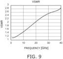
- FIG. 9 is a graph illustrating results of an electromagnetic field simulation when a terminal of 50 S2 is connected to the high frequency circuit board of the first comparative example.
- the vertical axis is the VSWR; and the horizontal axis is the frequency.
- the VSWR starts to degrade at several GHz or more due to the discontinuity of the line impedance of the second region 163 having the line width which becomes narrow and/or because the unnecessary inductance of the ground through-hole (height being 0.4 mm) is large.
- the VSWR is about 2.8 at 40 GHz; and the high frequency characteristics degrade.
- FIG. 10A is a schematic perspective view of a grounding structure of a high frequency circuit board according to a second embodiment
- FIG. 10B is a schematic plan view of the grounding structure
- FIG. 10C is a schematic cross-sectional view of the dielectric substrate along line A-A
- FIG. 10D is a schematic cross-sectional view in which first and second conductor layers are filled into the first through-hole.
- the first through-hole 13 includes a sidewall widening toward the second surface 12 from the boundary between the first opening 13a and the second opening 13b. Therefore, the thickness of the dielectric substrate 10 thins from the end portion of the second opening 13b (the thickness T1) toward the first opening 13a. Also, the line width of the taper region 62 of the microstripline upper electrode 65 becomes narrow toward the first opening 13a of the first through-hole 13. The characteristic impedance of the microstripline is dependent on the ratio of the line width and the dielectric substrate thickness.
- the inductance of a first grounding conductor layer 38 can be reduced while maintaining the ratio of the line width and the dielectric substrate thickness at a prescribed value toward the first opening 13a of the first through-hole 13 and while maintaining the impedance value at a prescribed value (e.g., 50 ⁇ ) by reducing these together.
- the thickness T1 of the dielectric substrate 10 is set to 0.4 mm, etc.
- the depth T3 of the first opening 13a can be set to 0.1 mm, etc.
- the line width W1 of the first region 61 of the microstripline 65 is set to 0.8 mm; and, for example, the line width W2 of the one end portion of the microstripline 65 is set to 0.2 mm, etc.
- the thermal resistance is reduced by filling a first conductor layer 80 inward of a first grounding conductor layer 38a provided at the sidewall of the first opening 13a because the first conductor layer 80 becomes a heat dissipation path.
- a second conductor layer 82 inward of a first grounding conductor layer 38b provided at the sidewall of the second opening 13b, the heat dissipation path widens further in a radial configuration downward; therefore, the generated heat is dissipated easily externally via a heat dissipation plate, etc.
- the second conductor layer 82 is a solder material, it is easy to closely adhere to the heat dissipation plate, etc.
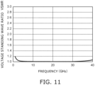
- FIG. 11 is a graph illustrating the frequency characteristics of the voltage standing wave ratio from an electromagnetic field simulation when a terminal of 50 S2 is connected to the high frequency substrate of the second embodiment.
- the voltage standing wave ratio is 1.03 or less in the bandwidth of 3 to 40 GHz, and is reduced compared to that of the first embodiment of FIG. 7B which is 1.2 or less at 3 to 40 GHz.
- the high frequency characteristics are improved because the ground inductance is reduced while setting the ratio of the thickness of the dielectric substrate to the microstripline width to the prescribed value.
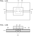
- FIG. 12A is a schematic plan view of a grounding structure of a high frequency circuit board according to a second comparative example; and FIG. 12B is a schematic cross-sectional view along line E-E.
- a grounding structure of a high frequency circuit board is provided in which the ground inductance is reduced, and the high frequency characteristics are improved in a high frequency band of several GHz or more. Therefore, the embodiments are widely applicable to microwave to millimeter-wave communication devices.
Landscapes
- Engineering & Computer Science (AREA)
- Microelectronics & Electronic Packaging (AREA)
- Structure Of Printed Boards (AREA)
- Physics & Mathematics (AREA)
- Geometry (AREA)
- Waveguides (AREA)
Claims (6)
- Erdungsstruktur einer Hochfrequenz-Leiterplatte (5, 7), umfassend:ein dielektrisches Substrat (10) mit einer ersten Oberfläche (11), einer zweiten Oberfläche (12) und einer ersten Durchgangsbohrung (13), wobei die zweite Oberfläche (12) an einer der ersten Oberfläche (11) gegenüberliegenden Seite vorgesehen ist, wobei eine erste Öffnung (13a) der ersten Durchgangsbohrung (13) an der ersten Oberfläche (11) kleiner ist als eine zweite Öffnung (13b) der ersten Durchgangsbohrung (13) an der zweiten Oberfläche (12);eine erste Erdungsleiterschicht (30, 38), die in der ersten Durchgangsbohrung (13) vorgesehen ist;eine Rückfläche-Erdungselektrode (40), die an der zweiten Oberfläche (12) vorgesehen und mit der ersten Erdungsleiterschicht (30) verbunden ist;eine obere Erdungselektrode (50), die an der ersten Oberfläche (11) vorgesehen und mindestens mit der ersten Erdungsleiterschicht (30) verbunden ist; undeine obere Mikrostreifenline-Elektrode (65), die an der ersten Oberfläche (11) vorgesehen ist, wobei die obere Mikrostripline-Elektrode (65) mindestens einen ersten Bereich (61) mit einer ersten Linienbreite (W1) enthält, wobei die obere Mikrostreifenline -Elektrode (65) einen Endabschnitt (63) aufweist, der der ersten Öffnung (13a) gegenübersteht und die zweite Öffnung (13b) überlappt, wobei eine zweite Linienbreite (W2) des einen Endabschnitts (63) schmaler ist als die erste Linienbreite (W1).
- Erdungsstruktur der Hochfrequenz-Leiterplatte (5, 7) nach Anspruch 1, wobei die erste Erdungsleiterschicht (30) eine Seitenwand (13c) der ersten Durchgangsbohrung (13) abdeckt.
- Erdungsstruktur der Hochfrequenz-Leiterplatte (5) nach Anspruch 1 oder 2, wobeidie obere Mikrostreifen-Elektrode (65) einen Verjüngungsbereich (62) zwischen dem ersten Bereich (61) und dem einen Endabschnitt enthält, undzwischen einem Endabschnitt der zweiten Öffnung (13b) und der ersten Öffnung (13a) ein Verhältnis zwischen einer Linienbreite des Verjüngungsbereichs (62) und einer Dicke des dielektrischen Substrats (10) auf einen vorgeschriebenen Wert eingestellt wird.
- Erdungsstruktur der Hochfrequenz-Leiterplatte (5) nach Anspruch 2, wobei eine erste Leiterschicht (80) nach innen von der ersten Erdungsleiterschicht (38a) an der Seitenwand (13c) der ersten Durchgangsbohrung (13) gefüllt ist.
- Erdungsstruktur der Hochfrequenz-Leiterplatte (5) nach Anspruch 4, wobei eine zweite Leiterschicht (82) in die zweite Öffnung (13b) der ersten Durchgangsbohrung (13) gefüllt ist.
- Erdungsstruktur der Hochfrequenz-Leiterplatte (5) nach Anspruch 5, wobei die zweite Leiterschicht (82) ein Lötmaterial enthält.
Applications Claiming Priority (2)
| Application Number | Priority Date | Filing Date | Title |
|---|---|---|---|
| JP2018190092 | 2018-10-05 | ||
| PCT/JP2019/020861 WO2020070919A1 (ja) | 2018-10-05 | 2019-05-27 | 高周波回路基板の接地構造 |
Publications (3)
| Publication Number | Publication Date |
|---|---|
| EP3863113A1 EP3863113A1 (de) | 2021-08-11 |
| EP3863113A4 EP3863113A4 (de) | 2022-07-27 |
| EP3863113B1 true EP3863113B1 (de) | 2024-10-09 |
Family
ID=70055437
Family Applications (1)
| Application Number | Title | Priority Date | Filing Date |
|---|---|---|---|
| EP19853252.5A Active EP3863113B1 (de) | 2018-10-05 | 2019-05-27 | Erdungsstruktur für eine hochfrequenz-leiterplatte |
Country Status (4)
| Country | Link |
|---|---|
| US (1) | US11252814B2 (de) |
| EP (1) | EP3863113B1 (de) |
| JP (1) | JP7171618B2 (de) |
| WO (1) | WO2020070919A1 (de) |
Families Citing this family (4)
| Publication number | Priority date | Publication date | Assignee | Title |
|---|---|---|---|---|
| US10950562B1 (en) * | 2018-11-30 | 2021-03-16 | Hrl Laboratories, Llc | Impedance-matched through-wafer transition using integrated heat-spreader technology |
| JP7644588B2 (ja) | 2020-11-27 | 2025-03-12 | 株式会社東芝 | 高周波基板 |
| US11300587B1 (en) * | 2020-12-21 | 2022-04-12 | Wanshih Electronic Co., Ltd. | High-frequency measurement line structure |
| EP4287253A1 (de) * | 2022-06-01 | 2023-12-06 | Aselsan Elektronik Sanayi ve Ticaret Anonim Sirketi | Qfn-kunststoffpackungssystem in chipgrösse für integrierte hochfrequenzschaltungen |
Family Cites Families (18)
| Publication number | Priority date | Publication date | Assignee | Title |
|---|---|---|---|---|
| JPS5846571Y2 (ja) | 1979-12-04 | 1983-10-24 | 富士通株式会社 | 高周波回路装置 |
| JPS59112701A (ja) | 1982-12-20 | 1984-06-29 | Matsushita Electric Ind Co Ltd | マイクロ波集積回路 |
| JPS6159764A (ja) | 1984-08-30 | 1986-03-27 | Fujitsu Ltd | マイクロ波リ−ドレスパツケ−ジの縦続接続構造 |
| JPH0236202U (de) | 1988-09-01 | 1990-03-08 | ||
| JPH03131102A (ja) | 1989-10-17 | 1991-06-04 | Mitsubishi Materials Corp | 半導体素子と回路基板又はキャリヤとの接続方法 |
| JPH04297085A (ja) * | 1991-03-13 | 1992-10-21 | Mitsubishi Electric Corp | 混成集積回路装置 |
| JPH05327323A (ja) | 1992-05-20 | 1993-12-10 | Matsushita Electric Ind Co Ltd | 共振器 |
| EP0718905A1 (de) * | 1994-12-21 | 1996-06-26 | Industrial Technology Research Institute | Überflächenmontierbare Mikrowellen-IC-Gehäuse |
| JPH0951209A (ja) * | 1995-08-08 | 1997-02-18 | Nippon Telegr & Teleph Corp <Ntt> | 誘電体基板および配線基板 |
| JP3897401B2 (ja) | 1997-06-12 | 2007-03-22 | 沖電気工業株式会社 | 高周波用チップキャリアおよびそれを用いた半導体光制御素子の実装構造 |
| JPH11145335A (ja) * | 1997-11-11 | 1999-05-28 | Toyota Central Res & Dev Lab Inc | 半導体装置及び半導体装置の製造方法 |
| JP2002313982A (ja) * | 2001-04-18 | 2002-10-25 | Matsushita Electric Ind Co Ltd | 半導体装置 |
| JP2010199392A (ja) * | 2009-02-26 | 2010-09-09 | Toshiba Corp | 高周波モジュール |
| JP2011172173A (ja) * | 2010-02-22 | 2011-09-01 | Hitachi Metals Ltd | ミリ波回路モジュール及びそれを用いたミリ波送受信機 |
| US9526184B2 (en) * | 2012-06-29 | 2016-12-20 | Viasystems, Inc. | Circuit board multi-functional hole system and method |
| US20160195432A1 (en) * | 2013-02-27 | 2016-07-07 | Electronics And Telecommunications Research Institute | Optical transceiver module |
| US20170318673A1 (en) * | 2016-04-29 | 2017-11-02 | Arista Networks, Inc. | Connector for printed circuit board |
| KR102390322B1 (ko) * | 2017-12-19 | 2022-04-26 | 삼성전자주식회사 | 안테나 장치를 포함하는 전자 장치 |
-
2019
- 2019-05-27 US US16/645,956 patent/US11252814B2/en active Active
- 2019-05-27 JP JP2019564121A patent/JP7171618B2/ja active Active
- 2019-05-27 EP EP19853252.5A patent/EP3863113B1/de active Active
- 2019-05-27 WO PCT/JP2019/020861 patent/WO2020070919A1/ja not_active Ceased
Also Published As
| Publication number | Publication date |
|---|---|
| JP7171618B2 (ja) | 2022-11-15 |
| US11252814B2 (en) | 2022-02-15 |
| WO2020070919A1 (ja) | 2020-04-09 |
| JPWO2020070919A1 (ja) | 2021-09-16 |
| US20200344874A1 (en) | 2020-10-29 |
| EP3863113A4 (de) | 2022-07-27 |
| EP3863113A1 (de) | 2021-08-11 |
Similar Documents
| Publication | Publication Date | Title |
|---|---|---|
| EP3863113B1 (de) | Erdungsstruktur für eine hochfrequenz-leiterplatte | |
| US7964937B2 (en) | Multilayer dielectric substrate and semiconductor package | |
| US12113293B2 (en) | Antenna-on-package including multiple types of antenna | |
| JP5323167B2 (ja) | パッケージ | |
| US10959358B2 (en) | Electronic component module | |
| JPWO2004051746A1 (ja) | 高周波回路および高周波パッケージ | |
| JPH10276113A (ja) | 超高周波帯無線通信装置 | |
| JP3829839B2 (ja) | 高周波パッケージ | |
| US6396342B1 (en) | Microwave amplifier generating distortion-reduced high output microwave power | |
| WO2015030093A1 (ja) | 素子収納用パッケージおよび実装構造体 | |
| US6507110B1 (en) | Microwave device and method for making same | |
| JP2018129596A (ja) | 無線装置 | |
| JP6001539B2 (ja) | 配線基板及びこれを用いた高周波モジュール | |
| US10637405B2 (en) | Wideband biasing of high power amplifiers | |
| US9805995B2 (en) | Element-accommodating package and mounting structure | |
| JP4137059B2 (ja) | 電子装置および半導体装置 | |
| CN107039356B (zh) | 微米波段及毫米波段封装体 | |
| US10110185B2 (en) | Microwave semiconductor device | |
| EP4579743A1 (de) | Mehrweg-leistungsverstärker mit kondensator zur kompensation einer kopplung zwischen verstärkerpfaden | |
| US12580288B2 (en) | Dielectric filter and dielectric resonator | |
| US20260066543A1 (en) | Multilayer substrate and antenna device | |
| US11874515B2 (en) | Electronic device | |
| JP6208618B2 (ja) | 素子実装基板および実装構造体 | |
| US20250175203A1 (en) | High frequency module and communication device | |
| JPH11214834A (ja) | 電子回路基板 |
Legal Events
| Date | Code | Title | Description |
|---|---|---|---|
| STAA | Information on the status of an ep patent application or granted ep patent |
Free format text: STATUS: UNKNOWN |
|
| STAA | Information on the status of an ep patent application or granted ep patent |
Free format text: STATUS: THE INTERNATIONAL PUBLICATION HAS BEEN MADE |
|
| PUAI | Public reference made under article 153(3) epc to a published international application that has entered the european phase |
Free format text: ORIGINAL CODE: 0009012 |
|
| STAA | Information on the status of an ep patent application or granted ep patent |
Free format text: STATUS: REQUEST FOR EXAMINATION WAS MADE |
|
| 17P | Request for examination filed |
Effective date: 20200409 |
|
| AK | Designated contracting states |
Kind code of ref document: A1 Designated state(s): AL AT BE BG CH CY CZ DE DK EE ES FI FR GB GR HR HU IE IS IT LI LT LU LV MC MK MT NL NO PL PT RO RS SE SI SK SM TR |
|
| DAV | Request for validation of the european patent (deleted) | ||
| DAX | Request for extension of the european patent (deleted) | ||
| A4 | Supplementary search report drawn up and despatched |
Effective date: 20220629 |
|
| RIC1 | Information provided on ipc code assigned before grant |
Ipc: H01L 23/498 20060101ALN20220623BHEP Ipc: H05K 3/34 20060101ALI20220623BHEP Ipc: H05K 1/02 20060101ALI20220623BHEP Ipc: H01P 5/02 20060101ALI20220623BHEP Ipc: H01P 3/08 20060101ALI20220623BHEP Ipc: H01P 3/00 20060101ALI20220623BHEP Ipc: H01L 23/12 20060101ALI20220623BHEP Ipc: H01L 23/66 20060101ALI20220623BHEP Ipc: H01P 5/08 20060101AFI20220623BHEP |
|
| GRAP | Despatch of communication of intention to grant a patent |
Free format text: ORIGINAL CODE: EPIDOSNIGR1 |
|
| STAA | Information on the status of an ep patent application or granted ep patent |
Free format text: STATUS: GRANT OF PATENT IS INTENDED |
|
| RIC1 | Information provided on ipc code assigned before grant |
Ipc: H01L 23/498 20060101ALN20240411BHEP Ipc: H05K 3/34 20060101ALI20240411BHEP Ipc: H05K 1/02 20060101ALI20240411BHEP Ipc: H01P 5/02 20060101ALI20240411BHEP Ipc: H01P 3/08 20060101ALI20240411BHEP Ipc: H01P 3/00 20060101ALI20240411BHEP Ipc: H01L 23/12 20060101ALI20240411BHEP Ipc: H01L 23/66 20060101ALI20240411BHEP Ipc: H01P 5/08 20060101AFI20240411BHEP |
|
| RIC1 | Information provided on ipc code assigned before grant |
Ipc: H01L 23/498 20060101ALN20240412BHEP Ipc: H05K 3/34 20060101ALI20240412BHEP Ipc: H05K 1/02 20060101ALI20240412BHEP Ipc: H01P 5/02 20060101ALI20240412BHEP Ipc: H01P 3/08 20060101ALI20240412BHEP Ipc: H01P 3/00 20060101ALI20240412BHEP Ipc: H01L 23/12 20060101ALI20240412BHEP Ipc: H01L 23/66 20060101ALI20240412BHEP Ipc: H01P 5/08 20060101AFI20240412BHEP |
|
| INTG | Intention to grant announced |
Effective date: 20240430 |
|
| GRAS | Grant fee paid |
Free format text: ORIGINAL CODE: EPIDOSNIGR3 |
|
| GRAA | (expected) grant |
Free format text: ORIGINAL CODE: 0009210 |
|
| STAA | Information on the status of an ep patent application or granted ep patent |
Free format text: STATUS: THE PATENT HAS BEEN GRANTED |
|
| AK | Designated contracting states |
Kind code of ref document: B1 Designated state(s): AL AT BE BG CH CY CZ DE DK EE ES FI FR GB GR HR HU IE IS IT LI LT LU LV MC MK MT NL NO PL PT RO RS SE SI SK SM TR |
|
| REG | Reference to a national code |
Ref country code: CH Ref legal event code: EP |
|
| REG | Reference to a national code |
Ref country code: DE Ref legal event code: R096 Ref document number: 602019060238 Country of ref document: DE |
|
| REG | Reference to a national code |
Ref country code: IE Ref legal event code: FG4D |
|
| REG | Reference to a national code |
Ref country code: LT Ref legal event code: MG9D |
|
| REG | Reference to a national code |
Ref country code: NL Ref legal event code: MP Effective date: 20241009 |
|
| REG | Reference to a national code |
Ref country code: AT Ref legal event code: MK05 Ref document number: 1731619 Country of ref document: AT Kind code of ref document: T Effective date: 20241009 |
|
| PG25 | Lapsed in a contracting state [announced via postgrant information from national office to epo] |
Ref country code: NL Free format text: LAPSE BECAUSE OF FAILURE TO SUBMIT A TRANSLATION OF THE DESCRIPTION OR TO PAY THE FEE WITHIN THE PRESCRIBED TIME-LIMIT Effective date: 20241009 |
|
| PG25 | Lapsed in a contracting state [announced via postgrant information from national office to epo] |
Ref country code: NL Free format text: LAPSE BECAUSE OF FAILURE TO SUBMIT A TRANSLATION OF THE DESCRIPTION OR TO PAY THE FEE WITHIN THE PRESCRIBED TIME-LIMIT Effective date: 20241009 |
|
| PG25 | Lapsed in a contracting state [announced via postgrant information from national office to epo] |
Ref country code: HR Free format text: LAPSE BECAUSE OF FAILURE TO SUBMIT A TRANSLATION OF THE DESCRIPTION OR TO PAY THE FEE WITHIN THE PRESCRIBED TIME-LIMIT Effective date: 20241009 Ref country code: IS Free format text: LAPSE BECAUSE OF FAILURE TO SUBMIT A TRANSLATION OF THE DESCRIPTION OR TO PAY THE FEE WITHIN THE PRESCRIBED TIME-LIMIT Effective date: 20250209 Ref country code: PT Free format text: LAPSE BECAUSE OF FAILURE TO SUBMIT A TRANSLATION OF THE DESCRIPTION OR TO PAY THE FEE WITHIN THE PRESCRIBED TIME-LIMIT Effective date: 20250210 |
|
| PG25 | Lapsed in a contracting state [announced via postgrant information from national office to epo] |
Ref country code: FI Free format text: LAPSE BECAUSE OF FAILURE TO SUBMIT A TRANSLATION OF THE DESCRIPTION OR TO PAY THE FEE WITHIN THE PRESCRIBED TIME-LIMIT Effective date: 20241009 |
|
| PG25 | Lapsed in a contracting state [announced via postgrant information from national office to epo] |
Ref country code: BG Free format text: LAPSE BECAUSE OF FAILURE TO SUBMIT A TRANSLATION OF THE DESCRIPTION OR TO PAY THE FEE WITHIN THE PRESCRIBED TIME-LIMIT Effective date: 20241009 |
|
| PG25 | Lapsed in a contracting state [announced via postgrant information from national office to epo] |
Ref country code: ES Free format text: LAPSE BECAUSE OF FAILURE TO SUBMIT A TRANSLATION OF THE DESCRIPTION OR TO PAY THE FEE WITHIN THE PRESCRIBED TIME-LIMIT Effective date: 20241009 |
|
| PG25 | Lapsed in a contracting state [announced via postgrant information from national office to epo] |
Ref country code: NO Free format text: LAPSE BECAUSE OF FAILURE TO SUBMIT A TRANSLATION OF THE DESCRIPTION OR TO PAY THE FEE WITHIN THE PRESCRIBED TIME-LIMIT Effective date: 20250109 |
|
| PG25 | Lapsed in a contracting state [announced via postgrant information from national office to epo] |
Ref country code: AT Free format text: LAPSE BECAUSE OF FAILURE TO SUBMIT A TRANSLATION OF THE DESCRIPTION OR TO PAY THE FEE WITHIN THE PRESCRIBED TIME-LIMIT Effective date: 20241009 Ref country code: LV Free format text: LAPSE BECAUSE OF FAILURE TO SUBMIT A TRANSLATION OF THE DESCRIPTION OR TO PAY THE FEE WITHIN THE PRESCRIBED TIME-LIMIT Effective date: 20241009 Ref country code: GR Free format text: LAPSE BECAUSE OF FAILURE TO SUBMIT A TRANSLATION OF THE DESCRIPTION OR TO PAY THE FEE WITHIN THE PRESCRIBED TIME-LIMIT Effective date: 20250110 |
|
| PG25 | Lapsed in a contracting state [announced via postgrant information from national office to epo] |
Ref country code: PL Free format text: LAPSE BECAUSE OF FAILURE TO SUBMIT A TRANSLATION OF THE DESCRIPTION OR TO PAY THE FEE WITHIN THE PRESCRIBED TIME-LIMIT Effective date: 20241009 |
|
| PG25 | Lapsed in a contracting state [announced via postgrant information from national office to epo] |
Ref country code: RS Free format text: LAPSE BECAUSE OF FAILURE TO SUBMIT A TRANSLATION OF THE DESCRIPTION OR TO PAY THE FEE WITHIN THE PRESCRIBED TIME-LIMIT Effective date: 20250109 |
|
| PG25 | Lapsed in a contracting state [announced via postgrant information from national office to epo] |
Ref country code: SM Free format text: LAPSE BECAUSE OF FAILURE TO SUBMIT A TRANSLATION OF THE DESCRIPTION OR TO PAY THE FEE WITHIN THE PRESCRIBED TIME-LIMIT Effective date: 20241009 |
|
| PG25 | Lapsed in a contracting state [announced via postgrant information from national office to epo] |
Ref country code: DK Free format text: LAPSE BECAUSE OF FAILURE TO SUBMIT A TRANSLATION OF THE DESCRIPTION OR TO PAY THE FEE WITHIN THE PRESCRIBED TIME-LIMIT Effective date: 20241009 |
|
| REG | Reference to a national code |
Ref country code: DE Ref legal event code: R097 Ref document number: 602019060238 Country of ref document: DE |
|
| PG25 | Lapsed in a contracting state [announced via postgrant information from national office to epo] |
Ref country code: EE Free format text: LAPSE BECAUSE OF FAILURE TO SUBMIT A TRANSLATION OF THE DESCRIPTION OR TO PAY THE FEE WITHIN THE PRESCRIBED TIME-LIMIT Effective date: 20241009 |
|
| PGFP | Annual fee paid to national office [announced via postgrant information from national office to epo] |
Ref country code: FR Payment date: 20250401 Year of fee payment: 7 |
|
| PG25 | Lapsed in a contracting state [announced via postgrant information from national office to epo] |
Ref country code: RO Free format text: LAPSE BECAUSE OF FAILURE TO SUBMIT A TRANSLATION OF THE DESCRIPTION OR TO PAY THE FEE WITHIN THE PRESCRIBED TIME-LIMIT Effective date: 20241009 |
|
| PG25 | Lapsed in a contracting state [announced via postgrant information from national office to epo] |
Ref country code: SK Free format text: LAPSE BECAUSE OF FAILURE TO SUBMIT A TRANSLATION OF THE DESCRIPTION OR TO PAY THE FEE WITHIN THE PRESCRIBED TIME-LIMIT Effective date: 20241009 |
|
| PG25 | Lapsed in a contracting state [announced via postgrant information from national office to epo] |
Ref country code: CZ Free format text: LAPSE BECAUSE OF FAILURE TO SUBMIT A TRANSLATION OF THE DESCRIPTION OR TO PAY THE FEE WITHIN THE PRESCRIBED TIME-LIMIT Effective date: 20241009 |
|
| PG25 | Lapsed in a contracting state [announced via postgrant information from national office to epo] |
Ref country code: IT Free format text: LAPSE BECAUSE OF FAILURE TO SUBMIT A TRANSLATION OF THE DESCRIPTION OR TO PAY THE FEE WITHIN THE PRESCRIBED TIME-LIMIT Effective date: 20241009 |
|
| PLBE | No opposition filed within time limit |
Free format text: ORIGINAL CODE: 0009261 |
|
| STAA | Information on the status of an ep patent application or granted ep patent |
Free format text: STATUS: NO OPPOSITION FILED WITHIN TIME LIMIT |
|
| PG25 | Lapsed in a contracting state [announced via postgrant information from national office to epo] |
Ref country code: SE Free format text: LAPSE BECAUSE OF FAILURE TO SUBMIT A TRANSLATION OF THE DESCRIPTION OR TO PAY THE FEE WITHIN THE PRESCRIBED TIME-LIMIT Effective date: 20241009 |
|
| 26N | No opposition filed |
Effective date: 20250710 |
|
| REG | Reference to a national code |
Ref country code: GB Ref legal event code: 732E Free format text: REGISTERED BETWEEN 20250911 AND 20250917 |
|
| REG | Reference to a national code |
Ref country code: DE Ref legal event code: R119 Ref document number: 602019060238 Country of ref document: DE |
|
| REG | Reference to a national code |
Ref country code: CH Ref legal event code: H13 Free format text: ST27 STATUS EVENT CODE: U-0-0-H10-H13 (AS PROVIDED BY THE NATIONAL OFFICE) Effective date: 20251223 |
|
| PG25 | Lapsed in a contracting state [announced via postgrant information from national office to epo] |
Ref country code: LU Free format text: LAPSE BECAUSE OF NON-PAYMENT OF DUE FEES Effective date: 20250527 |
|
| PG25 | Lapsed in a contracting state [announced via postgrant information from national office to epo] |
Ref country code: CH Free format text: LAPSE BECAUSE OF NON-PAYMENT OF DUE FEES Effective date: 20250531 |
|
| REG | Reference to a national code |
Ref country code: BE Ref legal event code: MM Effective date: 20250531 |
|
| PG25 | Lapsed in a contracting state [announced via postgrant information from national office to epo] |
Ref country code: MC Free format text: LAPSE BECAUSE OF FAILURE TO SUBMIT A TRANSLATION OF THE DESCRIPTION OR TO PAY THE FEE WITHIN THE PRESCRIBED TIME-LIMIT Effective date: 20241009 |
|
| PGFP | Annual fee paid to national office [announced via postgrant information from national office to epo] |
Ref country code: GB Payment date: 20260310 Year of fee payment: 8 |
|
| PG25 | Lapsed in a contracting state [announced via postgrant information from national office to epo] |
Ref country code: DE Free format text: LAPSE BECAUSE OF NON-PAYMENT OF DUE FEES Effective date: 20251202 Ref country code: IE Free format text: LAPSE BECAUSE OF NON-PAYMENT OF DUE FEES Effective date: 20250527 |
|
| PG25 | Lapsed in a contracting state [announced via postgrant information from national office to epo] |
Ref country code: BE Free format text: LAPSE BECAUSE OF NON-PAYMENT OF DUE FEES Effective date: 20250531 |