EP3919941A1 - Tranche de semi-conducteur, élément de détection de rayonnement, détecteur de rayonnement et procédé de production pour substrat monocristallin semi-conducteur composé - Google Patents
Tranche de semi-conducteur, élément de détection de rayonnement, détecteur de rayonnement et procédé de production pour substrat monocristallin semi-conducteur composé Download PDFInfo
- Publication number
- EP3919941A1 EP3919941A1 EP19929507.2A EP19929507A EP3919941A1 EP 3919941 A1 EP3919941 A1 EP 3919941A1 EP 19929507 A EP19929507 A EP 19929507A EP 3919941 A1 EP3919941 A1 EP 3919941A1
- Authority
- EP
- European Patent Office
- Prior art keywords
- resistivity
- monocrystal
- substrate
- detection element
- radiation detection
- Prior art date
- Legal status (The legal status is an assumption and is not a legal conclusion. Google has not performed a legal analysis and makes no representation as to the accuracy of the status listed.)
- Pending
Links
Images

Classifications
-
- C—CHEMISTRY; METALLURGY
- C30—CRYSTAL GROWTH
- C30B—SINGLE-CRYSTAL GROWTH; UNIDIRECTIONAL SOLIDIFICATION OF EUTECTIC MATERIAL OR UNIDIRECTIONAL DEMIXING OF EUTECTOID MATERIAL; REFINING BY ZONE-MELTING OF MATERIAL; PRODUCTION OF A HOMOGENEOUS POLYCRYSTALLINE MATERIAL WITH DEFINED STRUCTURE; SINGLE CRYSTALS OR HOMOGENEOUS POLYCRYSTALLINE MATERIAL WITH DEFINED STRUCTURE; AFTER-TREATMENT OF SINGLE CRYSTALS OR A HOMOGENEOUS POLYCRYSTALLINE MATERIAL WITH DEFINED STRUCTURE; APPARATUS THEREFOR
- C30B23/00—Single-crystal growth by condensing evaporated or sublimed materials
-
- C—CHEMISTRY; METALLURGY
- C30—CRYSTAL GROWTH
- C30B—SINGLE-CRYSTAL GROWTH; UNIDIRECTIONAL SOLIDIFICATION OF EUTECTIC MATERIAL OR UNIDIRECTIONAL DEMIXING OF EUTECTOID MATERIAL; REFINING BY ZONE-MELTING OF MATERIAL; PRODUCTION OF A HOMOGENEOUS POLYCRYSTALLINE MATERIAL WITH DEFINED STRUCTURE; SINGLE CRYSTALS OR HOMOGENEOUS POLYCRYSTALLINE MATERIAL WITH DEFINED STRUCTURE; AFTER-TREATMENT OF SINGLE CRYSTALS OR A HOMOGENEOUS POLYCRYSTALLINE MATERIAL WITH DEFINED STRUCTURE; APPARATUS THEREFOR
- C30B29/00—Single crystals or homogeneous polycrystalline material with defined structure characterised by the material or by their shape
- C30B29/10—Inorganic compounds or compositions
- C30B29/46—Sulfur-, selenium- or tellurium-containing compounds
- C30B29/48—AIIBVI compounds wherein A is Zn, Cd or Hg, and B is S, Se or Te
-
- H—ELECTRICITY
- H10—SEMICONDUCTOR DEVICES; ELECTRIC SOLID-STATE DEVICES NOT OTHERWISE PROVIDED FOR
- H10F—INORGANIC SEMICONDUCTOR DEVICES SENSITIVE TO INFRARED RADIATION, LIGHT, ELECTROMAGNETIC RADIATION OF SHORTER WAVELENGTH OR CORPUSCULAR RADIATION
- H10F30/00—Individual radiation-sensitive semiconductor devices in which radiation controls the flow of current through the devices, e.g. photodetectors
- H10F30/301—Individual radiation-sensitive semiconductor devices in which radiation controls the flow of current through the devices, e.g. photodetectors the devices being sensitive to very short wavelength, e.g. being sensitive to X-rays, gamma-rays or corpuscular radiation
-
- H—ELECTRICITY
- H10—SEMICONDUCTOR DEVICES; ELECTRIC SOLID-STATE DEVICES NOT OTHERWISE PROVIDED FOR
- H10F—INORGANIC SEMICONDUCTOR DEVICES SENSITIVE TO INFRARED RADIATION, LIGHT, ELECTROMAGNETIC RADIATION OF SHORTER WAVELENGTH OR CORPUSCULAR RADIATION
- H10F39/00—Integrated devices, or assemblies of multiple devices, comprising at least one element covered by group H10F30/00, e.g. radiation detectors comprising photodiode arrays
- H10F39/10—Integrated devices
- H10F39/12—Image sensors
- H10F39/18—Complementary metal-oxide-semiconductor [CMOS] image sensors; Photodiode array image sensors
- H10F39/189—X-ray, gamma-ray or corpuscular radiation imagers
-
- H—ELECTRICITY
- H10—SEMICONDUCTOR DEVICES; ELECTRIC SOLID-STATE DEVICES NOT OTHERWISE PROVIDED FOR
- H10F—INORGANIC SEMICONDUCTOR DEVICES SENSITIVE TO INFRARED RADIATION, LIGHT, ELECTROMAGNETIC RADIATION OF SHORTER WAVELENGTH OR CORPUSCULAR RADIATION
- H10F71/00—Manufacture or treatment of devices covered by this subclass
- H10F71/125—The active layers comprising only Group II-VI materials, e.g. CdS, ZnS or CdTe
- H10F71/1253—The active layers comprising only Group II-VI materials, e.g. CdS, ZnS or CdTe comprising at least three elements, e.g. HgCdTe
-
- H—ELECTRICITY
- H10—SEMICONDUCTOR DEVICES; ELECTRIC SOLID-STATE DEVICES NOT OTHERWISE PROVIDED FOR
- H10F—INORGANIC SEMICONDUCTOR DEVICES SENSITIVE TO INFRARED RADIATION, LIGHT, ELECTROMAGNETIC RADIATION OF SHORTER WAVELENGTH OR CORPUSCULAR RADIATION
- H10F77/00—Constructional details of devices covered by this subclass
- H10F77/10—Semiconductor bodies
- H10F77/12—Active materials
- H10F77/123—Active materials comprising only Group II-VI materials, e.g. CdS, ZnS or HgCdTe
- H10F77/1233—Active materials comprising only Group II-VI materials, e.g. CdS, ZnS or HgCdTe characterised by the dopants
-
- H—ELECTRICITY
- H10—SEMICONDUCTOR DEVICES; ELECTRIC SOLID-STATE DEVICES NOT OTHERWISE PROVIDED FOR
- H10F—INORGANIC SEMICONDUCTOR DEVICES SENSITIVE TO INFRARED RADIATION, LIGHT, ELECTROMAGNETIC RADIATION OF SHORTER WAVELENGTH OR CORPUSCULAR RADIATION
- H10F77/00—Constructional details of devices covered by this subclass
- H10F77/10—Semiconductor bodies
- H10F77/12—Active materials
- H10F77/123—Active materials comprising only Group II-VI materials, e.g. CdS, ZnS or HgCdTe
- H10F77/1237—Active materials comprising only Group II-VI materials, e.g. CdS, ZnS or HgCdTe having at least three elements, e.g. HgCdTe
-
- Y—GENERAL TAGGING OF NEW TECHNOLOGICAL DEVELOPMENTS; GENERAL TAGGING OF CROSS-SECTIONAL TECHNOLOGIES SPANNING OVER SEVERAL SECTIONS OF THE IPC; TECHNICAL SUBJECTS COVERED BY FORMER USPC CROSS-REFERENCE ART COLLECTIONS [XRACs] AND DIGESTS
- Y02—TECHNOLOGIES OR APPLICATIONS FOR MITIGATION OR ADAPTATION AGAINST CLIMATE CHANGE
- Y02P—CLIMATE CHANGE MITIGATION TECHNOLOGIES IN THE PRODUCTION OR PROCESSING OF GOODS
- Y02P70/00—Climate change mitigation technologies in the production process for final industrial or consumer products
- Y02P70/50—Manufacturing or production processes characterised by the final manufactured product
Definitions
- the present invention relates to a semiconductor wafer, a radiation detection element, a radiation detector, and method for producing a compound semiconductor monocrystalline substrate.
- CdZnTe cadmium zinc telluride
- CdZnTe Since CdZnTe is composed of elements having relatively large atomic numbers, it has a higher detection efficiency of radiation (hard X-rays and ⁇ -rays). Therefore, a radiation detector using the CdZnTe (hereinafter referred to as CdZnTe-based detector) can be made smaller and have higher performance than those using other compound semiconductors.
- the CdZnTe-based detector since the CdZnTe-based detector has a mechanism for directly converting radiation into an electric current, it has higher detection efficiency and energy resolution than those of a scintillator detector having an indirect operation mechanism via luminescence, represented by sodium iodide (Nal).
- CdZnTe has a larger band gap, it is not susceptible to heat and has a smaller leakage current during operation. Therefore, the CdZnTe-based detector can operate at room temperature, and the devise size can be decreased, and further an increased energy resolution can be exerted by applying a high bias current, as compared with a detector using silicon (Si) or germanium (Ge) which requires a cooling device to operate it (see Patent Literatures 1 and 2).
- Patent Literature 3 discloses a technique for providing a CdTe monocrystal having 10 8 to 10 9 ⁇ cm by doping with chlorine (CI) or indium (In).
- Patent literature 4 discloses a technique in which a resistivity value in the 10 11 ⁇ cm order can be achieved by subjecting an In-doped CdZnTe monocrystal at application of a bias voltage of 100 V to a two-step ingot annealing after monocrystal growth.
- Patent Literature 5 discloses a CdTe or CdZnTe substrate cut out from an ingot obtained by subjecting a CdZnTe monocrystal doped with In as in Patent Literature 4 to monocrystal growth, followed by ingot annealing while maintaining a Cd vapor pressure, wherein when a bias voltage of 0V, 700V and 900V is applied to the substrate, a resistivity is in the 10 7 ⁇ cm order, and a relative standard deviation of the resistivity in a substrate plane at 0 V is 20% or less.
- Patent Literatures 6 to 8 disclose a technique (wafer annealing) in which a substrate is cut out from a CdTe monocrystalline ingot and annealed for the substrate.
- Patent Literature 6 performs annealing at an elevated temperature close to a melting point of CdTe in an Ar atmosphere, thereby removing precipitates.
- Patent Literature 7 subjects a CdTe substrate to wafer annealing at two stages: a high-temperature annealing at about 700 °C and annealing at about 400 °C in vacuum.
- Patent Literature 8 subjects a CdTe substrate to two-stage low-temperature annealing at about 400 °C in vacuum.
- Patent Literature 9 discloses that an In-doped CdZnTe substrate is subjected to wafer annealing at about 300 °C in an inert gas atmosphere, and when a bias of 700 V is applied to the annealed CdZnTe, a resistivity is in the 10 11 ⁇ cm order.
- a substrate having a resistivity of 10 7 Qcm or more is obtained when a high voltage of 900 V is applied.
- Patent Literature 5 discloses that the resistivity of the CdZnTe substrate is in the 10 7 ⁇ cm order when bias voltages of 0 V, 700 V and 900 V are applied to the substrate, by subjecting the In-doped CdZnTe monocrystal to monocrystal growth, followed by ingot annealing while maintaining the Cd vapor pressure, as described above.
- a ratio (variation ratio) of the resistivity at application of 0 V to the resistivity at application of a voltage of 900 V is calculated as approximately 350 to 800, which causes a problem that the resistivity significantly varies when a high voltage of 900 V is applied from a state where no voltage is applied.
- an object of the present invention is to provide a stable CdZnTe monocrystalline substrate having a small leakage current even when a high voltage is applied and having a lower variation in resistivity with respect to variations in the applied voltage values.
- Another object of the present invention is to provide a method that can effectively produce the above CdTe-based monocrystalline substrate.
- the present inventors have found that a substrate which has a sufficiently high resistivity even when a high bias voltage is applied from a state where no voltage is applied, and which can reduce its variation range can be obtained by considering a chemical composition, dopant materials to be added, and annealing conditions involved in a carrier activation in a crystal for a compound monocrystal based on CdZnTe. Then, they have found that when it is formed into an element, a radiation detection element having stable performance can be produced, and have completed the present invention.
- the present invention relates to a semiconductor wafer comprising a cadmium zinc telluride monocrystal having a zinc concentration of 4.0 at% or more and 6.5 at% or less and a chlorine concentration of 0.1 ppm by mass or more and 5.0 ppm by mass or less, wherein the semiconductor wafer has a resistivity of 1.0 ⁇ 10 7 ⁇ cm or more and 1.0 ⁇ 10 8 ⁇ cm or less when a voltage of 900 V is applied, and wherein a ratio (variation ratio) of the resistivity at application of 0 V to the resistivity at application of a voltage of 900 V is 20% or less.
- the resistivity means a value determined by investigating a IV characteristic by gradually applying a voltage to an element structure of the CdZnTe monocrystalline substrate in which an electrode structure is formed, drawing a IV characteristic curve, and, from the IV characteristic curve, obtaining a resistivity when a micro-voltage (about 0.1 V) is applied as 0 V resistivity (hereinafter referred to as 0V resistivity) and a resistivity when 900 V is applied as 900 V resistivity.
- the present invention relates to a radiation detection element, comprising: a substrate cut out from the semiconductor wafer according to the embodiment of the present invention such that a main surface is rectangular; a common electrode formed on one main surface of the substrate; and a plurality of pixel electrodes formed in matrix on the other main surface of the substrate.
- the radiation detection element of the present invention has a resistivity of 1.0 ⁇ 10 7 Qcm or more and 1.0 ⁇ 10 8 ⁇ cm or less when a voltage of 900 V is applied, and wherein a ratio (variation ratio) of the resistivity at application of 0 V to the resistivity at application of a voltage of 900 V is 20% or less.
- the present invention relates to a radiation detector, comprising: the radiation detection element according to the embodiment of the present invention; a power source for applying a bias voltage to the radiation detection element, the power source being connected to the radiation detection element; and an amplification unit for amplifying an electric signal output from the radiation detection element, the amplification unit being connected to the radiation detection element.
- the present invention relates to a method for producing a compound semiconductor monocrystalline substrate, the substrate comprising a cadmium zinc telluride monocrystal having a zinc concentration of 4.0 at% or more and 6.5 at% or less and a chlorine concentration of 0.1 ppm by mass or more and 5.0 ppm by mass or less, the substrate having a resistivity of 1.0 ⁇ 10 7 ⁇ cm or more and 1.0 ⁇ 10 8 ⁇ cm or less when a voltage of 900 V is applied, wherein the method comprises:
- a semiconductor wafer having a high resistivity of 1.0 ⁇ 10 7 ⁇ cm or more and 1.0 ⁇ 10 8 ⁇ cm or less when a voltage of 900 V is applied, and a low ratio (variation ratio) of the resistivity at application of 0 V to the resistivity at application of a voltage of 900 V (resistivity at 0 V / resistivity at 900 V) of 20% or less, by both the action of a part (Zn and Cl) of the raw materials having doped amounts adjusted such that the concentrations are in a predetermined range in the monocrystal, and the heat treatment for 50 to 90 hours after the crystal growth step of the monocrystal, which is carried out under conditions where the temperature of the monocrystal placing position in the furnace is 385 to 400 °C, and the temperature of the Cd reservoir is room temperature in a series of steps, without opening the ampule in the furnace. Therefore, the use of a radiation detection element provided with a substrate cut
- a radiation detector 1 includes: a radiation detection element 2; a capacitor 3; an amplification unit 4; and the like.
- a substrate 21 forming the radiation detection element 2 is a cadmium zinc telluride (CdZnTe) monocrystal, which is a II-VI group compound semiconductor monocrystal, and a main surface of the substrate 21 is formed in a thin plate shape. Further, the main surface of the substrate 21 is parallel to a predetermined crystal plane (for example, a (111) plane).
- a predetermined crystal plane for example, a (111) plane
- a common electrode 22 is a thin film of a metal (for example, platinum (Pt)) and is formed so as to cover the entire one main surface (hereinafter, B surface 21b) of the substrate 21.
- a plurality of pixel electrodes 23 are thin metal films and provided on the other main surface of the substrate 21 (hereinafter referred to as A surface 21a), and are arranged in the form of matrix.
- both electrodes are collectively referred to as electrodes 22, 23.
- the radiation detection element 2 is configured such that a predetermined bias voltage is applied, by connecting the common electrode 22 to the ground (grounding) and connecting each pixel electrode 23 to a power supply (a control unit) 5. Further, each pixel electrode 23 is connected to the capacitor 3 and the amplification unit 4. Although FIG. 1 shows that only the rightmost pixel electrode is connected to the capacitor 3 and the amplification unit 4, the other pixel electrodes 23 are also connected to the capacitor 3 and the amplification unit 4.
- the radiation detection element 2 when the radiation detection element 2 receives radiation (hard X-rays or ⁇ -rays), the radiation detector 1 generates electron-hole pairs in the substrate 21, which are output from the pixel electrodes 23 as an ionizing current by the bias voltage applied to the radiation detection element 2. This ionization current is then converted into an electric signal via the capacitor 3 and the amplification unit 4, and output to a data generation unit 6.
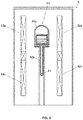
- the monocrystal growth furnace 9 is used in a vertical gradient freezing (VGF) method, and as shown in FIG. 2 , it includes: an outer monocrystal growth furnace body; a cadmium filling portion 91 for applying steam pressure; heaters 92; a quartz ampule 93; and the like.
- VVF vertical gradient freezing
- the heaters 92a, 92b are arranged in column inside the body, and each is configured to have a plurality of stages of heat generating portions. Each of the heaters 92a, 92b can independently set a heating temperature.
- the quartz ampoule 93 is comprised of a cylindrical crucible storage portion 93a and a tubular Cd reservoir portion 93b for controlling cadmium vapor pressure, which extends downward from a lower portion of the crucible storage portion 93a.
- the quartz ampoule 93 is arranged in the furnace body so that the crucible storage portion 93a is surrounded by the upper heater 92a and the Cd reservoir portion 93b is surrounded by the lower heater 92b.
- the method for producing the Cd(Zn)Te monocrystal according to the present embodiment includes: a preparation step; a crystal growth step; and a heat treatment step, and the method for producing the Cd(Zn)Te wafer includes: a cutting step; a wrapping step; and a mirror polishing step.
- the crucible is filled with a predetermined amount of Cd having a purity of 6N (99.99999%), Te having 6N, Zn and Cl which is a dopant material (impurity) as raw materials.
- Zn and Cl is added by adjusting the amount such that the Zn concentration in the monocrystal is 4.0 at% or more and 6.5 at% or less, and the Cl concentration is 0.1 ppm by mass or more and 5.0 ppm by mass or less.
- Cd is placed in the Cd reservoir portion 93b of the quartz ampoule 93, and the crucible filled with the raw materials is placed in the quartz ampoule 93.
- the quartz ampoule is then sealed in vacuum and the interior of the furnace is heated by the heaters 92a, 92b to synthesize the raw materials contained in the crucible.
- the interior of the furnace is further heated to melt the raw materials into a melt and the dopant is diffused into the melt.
- a vapor pressure of Cd is adjusted to about 0.12 to 0.14 MPa by controlling the temperature of the lower heater 92b, thereby suppressing the evaporation of Cd from the melt.
- the step proceeds to the crystal growth step.
- the output of each heat generating portion of the upper heater 92a which is composed of a plurality of stages in column, is adjusted so that a temperature gradient is generated so as to decrease the temperature from the lower end to the upper end of the melt.
- each heater is adjusted such that, at the upper portion of the melt, the temperature gradient is 0.05 to 1.0 °C/cm, and at the lower portion of the melt, the temperature gradient is about 1.0 to 5.0 °C/cm, which is higher than that of the upper portion in order to prevent the melt from instantaneously solidifying the raw material melt in the crucible in a temperature decreasing step during the growth of the monocrystal.
- the monocrystal is formed on the surface of the melt where the temperature is the lowest, and the monocrystal grows downward.
- the step proceeds to the heat treatment step.
- the temperature inside the furnace is decreased from the temperature at the end of the growth of the monocrystal to 385 °C to 400 °C by adjusting the temperature of each heat generation portion composed of a plurality of stages of the upper heater 92a while maintaining the grown CdZnTe monocrystal in the quartz ampule, and while maintaining the vapor pressure of Cd at a predetermined pressure by controlling the temperature of the lower heater 92b.
- the CdZnTe monocrystal is subjected to a heat treatment (ingot annealing) for 50 to 90 hours under conditions where the temperature of the Cd reservoir portion 93b is room temperature, without opening the ampoule (quartz ampoule 93) in the furnace.
- the sliced wafer-shaped substrate is subjected to the heat treatment (wafer annealing) at 275 to 325 °C for 10 to 25 hours in an inert atmosphere, and an electrode is formed on the CdZnTe monocrystal substrate after the wafer annealing to achieve a high resistivity of 1 ⁇ 10 11 ⁇ cm or more when a voltage of 900 V is applied.
- the variation in the resistivity is lower with respect to the variations in the applied voltages, and the stable resistivity can be maintained for the variations in the applied voltages, and, in particular, even if a higher voltage of 900V is applied, the variation ratio of the resistivities is lower, and when used for a radiation detection element, the variation in the resistivity during high-bias operation for detecting a small amount of radiation is lower and the generation of noise due to leakage current can be suppressed.
- the step proceeds to the cutting step.
- the cutting step the CdZnTe monocrystal ingot is sliced into a wafer shape along a predetermined crystal plane, and a plurality of wafers are cut out.
- the step proceeds to the wrapping step.
- the cut surface of each cut wafer is polished with a wrapping abrasive to remove irregularities.
- the step proceeds to the mirror polishing step.
- the polished surface of each wafer is polished with an abrasive for mirror polishing to finish it as a mirror surface.
- the CdZnTe wafer is composed of a cadmium zinc telluride monocrystal having a zinc concentration of 4.0 at% or more and 6.5 at% or less and a chlorine concentration of 0.1 ppm by mass or more and 5.0 ppm by mass or less.
- the CdZnTe wafer has a high resistivity of 1.0 ⁇ 10 7 ⁇ cm or more and 1.0 ⁇ 10 8 ⁇ cm or less when a voltage of 900 V is applied, and a lower ratio (variation ratio) of the resistivity at application of 0 V to the resistivity at application of a voltage of 900 V (resistivity at 0 V / resistivity at 900 V) of 20% or less.
- the radiation detection element 2 according to the present embodiment is produced through an electrode forming step, a dicing step, and an element resistivity measuring step.
- the above CdZnTe wafer is washed to remove foreign substances adhering to the surface.
- a photoresist is then applied to the polished surface of the CdZnTe wafer, and the photoresist is exposed using a photomask on which pixel electrode patterns is drawn.
- the development is then carried out to remove the exposed photoresist.
- the CdZnTe wafer is then immersed in a plating solution, and a metal is deposited onto positions where the photoresist has been removed, of the polished surfaces 21a, 21b of the CdZnTe wafer to form thin film layers. These thin film layers are grown to a predetermined film thickness to form the electrodes 22, 23. After the electrodes 22, 23 are formed, any unnecessary photoresist is removed, and the CdZnTe wafer is washed and dried.
- the step proceeds to the dicing step.
- the CdZnTe wafer in which the electrodes 22, 23 are formed on the polished surfaces 21a, 21b is cut and divided into a plurality of substrates 21, and the individual radiation detection elements 2 are cut out from the CdZnTe wafers.
- a sample for evaluation is obtained from the cut-out elements, and a voltage is applied to the sample to measure the element resistivity.
- the CdZnTe wafer can have a resistivity of 1.0 ⁇ 10 7 ⁇ cm or more and 1.0 ⁇ 10 8 ⁇ cm or less when a voltage of 900 V is applied, and a lower ratio (variation ratio) of the resistivity at application of 0 V to the resistivity at application of a voltage of 900 V (resistivity at 0 V / resistivity at 900 V) of 20% or less, so that the detection performance of the radiation detection element 2 is improved.
- Examples 1 to 3 and Comparative Examples 1 to 3 were produced by the above method for producing the monocrystal, and ingot annealing under the conditions of Examples 1 to 3 was carried out, and ingot annealing under the conditions of Comparative Examples 1 to 3 was carried out, and the CdZnTe monocrystals after the ingot annealing were taken out from the interior of the quartz ampule.
- Each ingot was then cut along the (111) plane to cut out a disk-shaped wafer, and a square substrate is further cut out from each wafer, and to produce an electrode on each substrate, a common electrode was formed from Pt on one main surface (B surface), and pixel electrodes were formed from Pt on the other main surface (A surface), and each substrate was diced to produce an ohmic type radiation detection element. Subsequently, the IV characteristic of each element was investigated by gradually applying a voltage to each element, and the IV characteristic curve was drawn.
- the resistivity when a micro-voltage (about 0.1V) was applied (hereinafter referred to as 0V resistivity) and the resistivity when voltages of 100V, 250V, 500V, 700V, 900V were applied were calculated.
- Table 1 summarizes the production conditions of each ingot, the characteristics of the wafer obtained from each ingot, the characteristics of the substrate cut out from each wafer and of the radiation detection element produced from each substrate.
- the measurement of the resistivity of each substrate was carried out by using a measuring device called COREMA-WT (contactless voltage mapping) from SEMIMAP SCIENTIFIC INSTRUMENTS, dividing the substrate into a plurality of fine parts (pixels) arranged in matrix along the main surface, measuring the resistivity for each part (hereinafter, referred to as a local resistivity), and obtaining an average value of the local resistivities (hereinafter, referred to as a resistivity of a substrate), thereby obtaining a resistivity at each applied voltage.
- COREMA-WT contactless voltage mapping
- Example 1 a CdZnTe monocrystal ingot was grown from a CdZnTe melt having a Zn concentration of 5 at% and a Cl concentration of 100 wtppm by the VGF method.
- the temperature of the monocrystal placing position was set to 385 °C from the end temperature of the monocrystal growth, and the temperature of the Cd reservoir portion was set to room temperature without opening the quartz ampule in the furnace, and the ingot annealing was carried out for 90 hours. After the ingot annealing, the ingot was cooled to room temperature to produce a CdZnTe monocrystal ingot.
- Example 1 a substrate having a square main surface of 4.0 mm ⁇ 4.0 mm and a thickness of 1.4 mm was cut out from the upper portion of the ingot according to Example 1 (solidification rate of 0.19).
- the composition of this substrate was examined, indicating that as shown in Table 1, the Zn ratio was 6.1 at% and the Cl concentration was 1.2 wtppm, which were within the range of the present invention.
- a common electrode was formed from Pt on one main surface (B surface) and pixel electrodes were formed from Pt on the other main surface (A surface) to produce an ohmic type radiation detection element.
- the IV characteristic curve of the radiation detection element was drawn and calculated, indicating that the resistivity at application of 0 V was 2.9 ⁇ 10 8 ⁇ cm, and the resistivity at application of 900 V was 2.0 ⁇ 10 7 ⁇ cm.
- the variation rate resistivity at 0V / resistivity at 900V was 14.8%.
- Example 2 a CdZnTe monocrystal ingot was grown from a CdZnTe melt having a Zn concentration of 5 at% and a Cl concentration of 100 wtppm.
- the temperature of the monocrystal placing position was set to 390 °C from the end temperature of the monocrystal growth, and the temperature of the Cd reservoir portion was set to room temperature without opening the quartz ampule in the furnace, and the ingot annealing was carried out for 90 hours. After the ingot annealing, the ingot was cooled to room temperature to produce a CdZnTe monocrystal ingot.
- Example 2 a substrate having a square main surface of 4.0 mm ⁇ 4.0 mm and a thickness of 1.4 mm was cut out from the upper portion of the ingot according to Example 2 (solidification rate of 0.75).
- the composition of this substrate was examined, indicating that as shown in Table 1, the Zn ratio was 4.3 at% and the Cl concentration was 3.9 wtppm, which were within the range of the present invention.
- a common electrode was formed from Pt on one main surface (B surface) and pixel electrodes were formed from Pt on the other main surface (A surface) to produce an ohmic type radiation detection element.
- the IV characteristic curve of the radiation detection element was drawn and calculated, indicating that the resistivity at application of 0 V was 6.4 ⁇ 10 8 ⁇ cm, and the resistivity at application of 900 V was 5.5 ⁇ 10 7 ⁇ cm.
- the variation rate resistivity at 0V / resistivity at 900V was 11.6%.
- Example 3 a CdZnTe monocrystal ingot was grown from a CdZnTe melt having a Zn concentration of 5 at% and a Cl concentration of 200 wtppm.
- the temperature of the monocrystal placing position was set to 400 °C from the end temperature of the monocrystal growth, and the temperature of the Cd reservoir portion was set to room temperature without opening the quartz ampule in the furnace, and the ingot annealing was carried out for 50 hours. After the ingot annealing, the ingot was cooled to room temperature to produce a CdZnTe monocrystal ingot.
- Example 3 a substrate having a square main surface of 4.0 mm ⁇ 4.0 mm and a thickness of 1.4 mm was cut out from the upper portion of the ingot according to Example 3 (solidification rate of 0.20).
- the composition of this substrate was examined, indicating that as shown in Table 1, the Zn ratio was 6.1 at% and the Cl concentration was 2.5 wtppm, which were within the range of the present invention.
- a common electrode was formed from Pt on one main surface (B surface) and pixel electrodes were formed from Pt on the other main surface (A surface) to produce an ohmic type radiation detection element.
- the IV characteristic curve of the radiation detection element was drawn and calculated, indicating that the resistivity at application of 0 V was 5.8 ⁇ 10 8 ⁇ cm, and the resistivity at application of 900 V was 3.9 ⁇ 10 7 ⁇ cm.
- the variation rate resistivity at 0V / resistivity at 900V was 15.0%.
- a CdZnTe monocrystal ingot was grown from a CdZnTe melt having a Zn concentration of 5 at% and a Cl concentration of 100 wtppm.
- the temperature of the monocrystal placing position was set to 950 °C from the end temperature of the monocrystal growth, and the temperature of the Cd reservoir was set to room temperature without opening the quartz ampule in the furnace, and the ingot annealing was carried out for 20 hours. After the ingot annealing, the ingot was cooled to room temperature to produce a CdZnTe monocrystal ingot.
- a common electrode was formed from Pt on one main surface (B surface) and pixel electrodes were formed from Pt on the other main surface (A surface) to produce an ohmic type radiation detection element.
- the IV characteristic curve of the radiation detection element was drawn and calculated, indicating that the resistivity at application of 0 V was 1.1 ⁇ 10 9 ⁇ cm, and the resistivity at application of 900 V was significantly decreased to 3.5 ⁇ 10 5 ⁇ cm.
- the variation rate resistivity at 0V / resistivity at 900V was about 3168%.
- the annealing temperature of the ingot annealing was higher, i.e., 950 °C, and the produced CdZnTe monocrystalline substrate had a higher variation ratio of the resistivity at application of 900 V.
- a CdZnTe monocrystal ingot was grown from a CdZnTe melt having a Zn concentration of 5 at% and a Cl concentration of 100 wtppm.
- the temperature of the monocrystal placing position was set to 410 °C from the end temperature of the monocrystal growth, and the temperature of the Cd reservoir portion was set to room temperature without opening the quartz ampule in the furnace, and the ingot annealing was carried out for 90 hours. After the ingot annealing, the ingot was cooled to room temperature to produce a CdZnTe monocrystal ingot.
- a common electrode was formed from Pt on one main surface (B surface) and pixel electrodes were formed from Pt on the other main surface (A surface) to produce an ohmic type radiation detection element.
- the IV characteristic curve of the radiation detection element was drawn and calculated, indicating that the resistivity at application of 0 V was 5.7 ⁇ 10 8 ⁇ cm, and the resistivity at application of 900 V was 2.3 ⁇ 10 7 ⁇ cm.
- the variation rate resistivity at 0V / resistivity at 900V was 24.7%.
- the temperature of the ingot annealing was 410 °C, which was higher than that of Examples 1 to 3.
- the resistivity of the produced CdZnTe monocrystalline substrate when 900 V was applied had a slightly higher variation range than the resistivity when 0 V was applied, with a decrease of about 25%, and the variation range with respect to the applied voltage was beyond a permissible range in terms of the stability of electrical characteristics.
- a CdZnTe monocrystal ingot was grown from a CdZnTe melt having a Zn concentration of 5 at% and a Cl concentration of 100 wtppm.
- the temperature of the monocrystal placing position was set to 378 °C from the end temperature of the monocrystal growth, and the temperature of the Cd reservoir portion was set to room temperature without opening the quartz ampule in the furnace, and the ingot annealing was carried out for 90 hours. After the ingot annealing, the ingot was cooled to room temperature to produce a CdZnTe monocrystal ingot.
- a common electrode was formed from Pt on one main surface (B surface) and pixel electrodes were formed from Pt on the other main surface (A surface) to produce an ohmic type radiation detection element.
- the IV characteristic curve of the radiation detection element was drawn and calculated, indicating that the resistivity at application of 0 V was 1.6 ⁇ 10 9 ⁇ cm, and the resistivity at application of 900 V was 3.6 ⁇ 10 7 ⁇ cm.
- the variation rate resistivity at 0V / resistivity at 900V was 43.0%.
- the temperature of the ingot annealing was 378 °C, which was lower than that of Examples 1 to 3.
- the resistivity of the produced CdZnTe monocrystalline substrate when 900 V was applied had a slightly higher variation range than the resistivity when 0 V was applied, with a decrease of about 43.0%, and the variation range with respect to the applied voltage was beyond a permissible range in terms of the stability of electrical characteristics.
- the substrates of Comparative Examples 1 to 3 had a variation ratio of from 24.7 to 3167.9%, whereas those of Examples 1 to 3 had a variation ratio of from 11.6 to 15.0%, which were lower values of 20% or less.
- the substrate produced by the production method according to the present embodiment has a lower ratio (variation ratio) of the resistivity at application of 0 V to the resistivity at application of a voltage of 900 V of 20%, as compared with the substrate produced by the conventional production method.
- the radiation detection elements according to Examples 1 to 3 have an extremely high 900V resistivity of 2.0 to 5.5 ⁇ 10 7 ⁇ cm, and a lower ratio (variation ratio) of the resistivity at application of 0 V to the resistivity at application of a voltage of 900 V of 20% or less, resulting in a stable value of the resistivity with respect to the variations in the applied voltages.
- the radiation detection elements according to Examples 1 to 3 have a higher 900 V resistivity and have characteristics suitable for allowing a stable ionizing current to flow at any voltage.
- Table 1 shows the production conditions and evaluation results of each Example and each Comparative Example. Table 1 Growth Conditions of Monocrystals Substrate Characteristics Characteristics of Radiation Detection Elements Variation Ratio : 0V/900V Monocrystal Doped Amount Heat Treatment Conditions Solidification Rate Dopant Theoretical Value Element Resistivity ( ⁇ cm) Zn (at%) Cl (wtppm) Temp.
- Example 1 Cd 1-x Zn z Te 5 100 385 90 0.19 6.1 1.2 2.9E+08 1.4E+08 8.7E+07 4.3E+07 2.9E+07 2.0E+07 14.8
- Example 2 Cd 1-x Zn z Te 5 100 390 90 0.75 4.3 3.9 6.4E+08 4.9E+08 3.1E+08 1.5E+08 8.9E+07 5.5E+07 11.6
- Example 3 Cd 1-x Zn z Te 5 200 400 50 0.2 6.1 2.5 5.8E+08 4.0E+08 2.4E+08 1.0E+08 6.2E+07 3.9E+07 15.0 Comparative Example 1 Cd 1-x Zn z Te 5 100 950 20 0.22 6.0 1.3 1.1E+09 1.1E+08 1.9E+07 1.6E+06 2.6E+07 3.5E+05 3167.9 Comparative Example 1 Cd 1-x Zn z Te 5 100 950 20 0.22 6.0 1.3 1.1E+09 1.1E+08
- an amount of a part of the raw materials is adjusted such that the concentrations in the monocrystal are within a predetermined range (zinc concentration is 4.0 at% or more and 6.5 at% or more, and the chlorine concentration is 0.1 ppm by mass or more and 5.0 ppm by mass or less) to grow the CdZnTe monocrystal, and after the crystal growth step of the single crystal is completed, the heat treatment is carried out for 50 to 90 hours under the conditions where the temperature of the monocrystal placing position in the furnace is 385 to 400 °C , and the temperature of the Cd reservoir portion is room temperature without opening the ampule in the furnace, whereby the CdZnTe wafer can be obtained which has the higher resistivity at application of a voltage of 900 V of 1.0 ⁇ 10 7 ⁇ cm or more and 1.0 ⁇ 10 8 ⁇ cm or less, and the lower ratio (variation ratio) of the resistivity at application
- the use of the radiation detection element 2 provided with the substrate 21 cut out from the CdZnTe wafer can allow a stable resistivity to be maintained for each voltage application value even if a higher bias voltage is applied, thereby suppressing generation of a large amount of leakage current.
- the radiation detection performance can be improved in the radiation detector 1 provided with the radiation detection element 2 using the CdZnTe monocrystal as a substrate.
- the shape of the main surface of the substrate 21 is square, but it may be rectangular or other shapes, and the number and arrangement of the pixel electrodes 23 may be determined depending on the size and shape of the main surface 21a.
- each of the main surfaces 21a, 21b of the substrate is the (111) plane, but other crystal planes may be used.
- each of the common electrode 22 and the pixel electrode 23 is formed from Pt, but it may be made of gold (Au) or other metals, or an alloy containing these metals. Furthermore, one of the common electrode 22 and the pixel electrode 23 may be formed from a metal different from the other (for example, the common electrode 22 is formed from indium (In) and the pixel electrode 23 is formed from Pt).
- the circuit provided between the radiation detection element 2 and the data generation unit 6 may have any configuration as long as a predetermined electric signal can be obtained.
Landscapes
- Chemical & Material Sciences (AREA)
- Organic Chemistry (AREA)
- Engineering & Computer Science (AREA)
- Crystallography & Structural Chemistry (AREA)
- Materials Engineering (AREA)
- Metallurgy (AREA)
- Inorganic Chemistry (AREA)
- Measurement Of Radiation (AREA)
- Crystals, And After-Treatments Of Crystals (AREA)
- Light Receiving Elements (AREA)
- Solid State Image Pick-Up Elements (AREA)
- Health & Medical Sciences (AREA)
- Toxicology (AREA)
Applications Claiming Priority (2)
| Application Number | Priority Date | Filing Date | Title |
|---|---|---|---|
| JP2019094049 | 2019-05-17 | ||
| PCT/JP2019/047671 WO2020235123A1 (fr) | 2019-05-17 | 2019-12-05 | Tranche de semi-conducteur, élément de détection de rayonnement, détecteur de rayonnement et procédé de production pour substrat monocristallin semi-conducteur composé |
Publications (2)
| Publication Number | Publication Date |
|---|---|
| EP3919941A1 true EP3919941A1 (fr) | 2021-12-08 |
| EP3919941A4 EP3919941A4 (fr) | 2022-11-02 |
Family
ID=73458526
Family Applications (1)
| Application Number | Title | Priority Date | Filing Date |
|---|---|---|---|
| EP19929507.2A Pending EP3919941A4 (fr) | 2019-05-17 | 2019-12-05 | Tranche de semi-conducteur, élément de détection de rayonnement, détecteur de rayonnement et procédé de production pour substrat monocristallin semi-conducteur composé |
Country Status (4)
| Country | Link |
|---|---|
| US (1) | US11967659B2 (fr) |
| EP (1) | EP3919941A4 (fr) |
| JP (1) | JP7250919B2 (fr) |
| WO (1) | WO2020235123A1 (fr) |
Families Citing this family (4)
| Publication number | Priority date | Publication date | Assignee | Title |
|---|---|---|---|---|
| WO2020235124A1 (fr) * | 2019-05-17 | 2020-11-26 | Jx金属株式会社 | Tranche de semi-conducteur, élément de détection de rayonnement, détecteur de rayonnement et procédé de production destinés à un substrat monocristallin semi-conducteur composé |
| CN114808135B (zh) * | 2022-05-16 | 2023-09-26 | 合肥天曜新材料科技有限公司 | 一种具有梯度电阻的czt晶锭生产方法 |
| CN116536768B (zh) * | 2023-06-29 | 2023-09-29 | 浙江珏芯微电子有限公司 | 一种碲锌镉单晶的生长用坩埚及生长方法 |
| CN118448516B (zh) * | 2024-06-11 | 2024-12-03 | 北京智创芯源科技有限公司 | 一种多片碲锌镉复合衬底、其制备方法及应用 |
Family Cites Families (12)
| Publication number | Priority date | Publication date | Assignee | Title |
|---|---|---|---|---|
| JPS6018532B2 (ja) | 1977-07-28 | 1985-05-10 | 東ソー株式会社 | 管状体の多数並行製造方法 |
| JPS63185898A (ja) | 1986-09-26 | 1988-08-01 | Nippon Mining Co Ltd | 高抵抗CdTe結晶及びその作成方法 |
| JPH0796478B2 (ja) | 1991-12-09 | 1995-10-18 | 株式会社ジャパンエナジー | CdTe単結晶の製造方法 |
| JPH09124310A (ja) | 1995-10-27 | 1997-05-13 | Sumitomo Metal Mining Co Ltd | CdTe結晶の製造方法 |
| JP4624648B2 (ja) | 2003-02-07 | 2011-02-02 | Jx日鉱日石金属株式会社 | 電気光学素子用CdTe系化合物半導体単結晶 |
| FR2905706B1 (fr) | 2006-09-07 | 2009-04-17 | Commissariat Energie Atomique | Procede d'elimination par recuit des precipites dans un materiau semi conducteur ii vi |
| DE102010006452B4 (de) | 2010-02-01 | 2012-01-26 | Siemens Aktiengesellschaft | Strahlenwandlermaterial, Strahlenwandler, Strahlendetektor, Verwendung eines Strahlenwandlermaterials und Verfahren zur Herstellung eines Strahlenwandlermaterials |
| CN103917897B (zh) | 2011-11-09 | 2016-08-17 | 皇家飞利浦有限公司 | 具有电荷排斥段间隙的辐射敏感探测器设备 |
| JP5953116B2 (ja) | 2012-05-18 | 2016-07-20 | Jx金属株式会社 | 放射線検出素子用化合物半導体結晶、放射線検出素子、および放射線検出器 |
| JP6018532B2 (ja) | 2013-03-29 | 2016-11-02 | Jx金属株式会社 | 半導体ウエハ、放射線検出素子、放射線検出器、および化合物半導体単結晶の製造方法 |
| JP6310794B2 (ja) * | 2014-07-11 | 2018-04-11 | Jx金属株式会社 | 放射線検出素子、放射線検出器および放射線検出素子の製造方法 |
| JP6713341B2 (ja) | 2016-04-28 | 2020-06-24 | Jx金属株式会社 | 化合物半導体基板およびその製造方法 |
-
2019
- 2019-12-05 EP EP19929507.2A patent/EP3919941A4/fr active Pending
- 2019-12-05 US US17/439,207 patent/US11967659B2/en active Active
- 2019-12-05 WO PCT/JP2019/047671 patent/WO2020235123A1/fr not_active Ceased
- 2019-12-05 JP JP2021520037A patent/JP7250919B2/ja active Active
Also Published As
| Publication number | Publication date |
|---|---|
| WO2020235123A1 (fr) | 2020-11-26 |
| US11967659B2 (en) | 2024-04-23 |
| JP7250919B2 (ja) | 2023-04-03 |
| JPWO2020235123A1 (fr) | 2020-11-26 |
| EP3919941A4 (fr) | 2022-11-02 |
| US20220199841A1 (en) | 2022-06-23 |
Similar Documents
| Publication | Publication Date | Title |
|---|---|---|
| US11967659B2 (en) | Semiconductor wafer, radiation detection element, radiation detector, and production method for compound semiconductor monocrystalline substrate | |
| Toufanian et al. | Cesium lead bromide semiconductor radiation detectors: crystal growth, detector performance and polarization | |
| JP5953116B2 (ja) | 放射線検出素子用化合物半導体結晶、放射線検出素子、および放射線検出器 | |
| JP6310794B2 (ja) | 放射線検出素子、放射線検出器および放射線検出素子の製造方法 | |
| US12021160B2 (en) | Semiconductor wafer, radiation detection element, radiation detector, and production method for compound semiconductor monocrystalline substrate | |
| JP6018532B2 (ja) | 半導体ウエハ、放射線検出素子、放射線検出器、および化合物半導体単結晶の製造方法 | |
| JP2022113874A (ja) | テルル化亜鉛カドミウム単結晶基板およびその製造方法 | |
| WO2008054840A9 (fr) | Compositions de matériaux semi-conducteurs dopés, codopés et tridopés | |
| JP6097854B2 (ja) | 放射線検出素子用化合物半導体結晶の製造方法 | |
| Li et al. | A new method for growing detector-grade cadmium zinc telluride crystals | |
| JP6713341B2 (ja) | 化合物半導体基板およびその製造方法 | |
| JP7217715B2 (ja) | 化合物半導体基板およびその製造方法 | |
| US20160299238A1 (en) | Radiation detector | |
| JP6725212B2 (ja) | CdTe系化合物半導体及びそれを用いた放射線検出素子 | |
| JP6366418B2 (ja) | CdTe又はCdZnTeからなるチップ基板、及びそれを用いた放射線検出器及び放射線検出器の製造方法 | |
| JPH06345598A (ja) | 放射線検出素子用CdTe結晶およびその製造方法 | |
| CN111900213B (zh) | 一种CdMnTe成像探测器的制备方法 | |
| Zaiour et al. | Preparation of High Purity CdTe for Nuclear Detector: Electrical and Nuclear Characterization | |
| Pak et al. | Characterization of Cd 0.9 Zn 0.1 Te single crystals for radiation detectors | |
| Roy et al. | Unseeded growth of CdZnTe: In by THM technique | |
| WO2025158701A1 (fr) | Élément de détection de rayonnement, détecteur de rayonnement et procédé de production de l'élément de détection de rayonnement | |
| JP2019212928A (ja) | CdTe系化合物半導体及びそれを用いた放射線検出素子 | |
| Swain et al. | Large volume single crystal growth of cadmium zinc telluride with minimal secondary phases for room temperature radiation detector application | |
| Davidov et al. | Preliminary results of characterization of CdZnTe crystals grown by the Davidov-Markov method | |
| Egarievwe et al. | Ampoule carbon coating and defects in CdMnTe crystals intended for applications in nuclear radiation detection |
Legal Events
| Date | Code | Title | Description |
|---|---|---|---|
| STAA | Information on the status of an ep patent application or granted ep patent |
Free format text: STATUS: THE INTERNATIONAL PUBLICATION HAS BEEN MADE |
|
| PUAI | Public reference made under article 153(3) epc to a published international application that has entered the european phase |
Free format text: ORIGINAL CODE: 0009012 |
|
| STAA | Information on the status of an ep patent application or granted ep patent |
Free format text: STATUS: REQUEST FOR EXAMINATION WAS MADE |
|
| 17P | Request for examination filed |
Effective date: 20210904 |
|
| AK | Designated contracting states |
Kind code of ref document: A1 Designated state(s): AL AT BE BG CH CY CZ DE DK EE ES FI FR GB GR HR HU IE IS IT LI LT LU LV MC MK MT NL NO PL PT RO RS SE SI SK SM TR |
|
| DAV | Request for validation of the european patent (deleted) | ||
| DAX | Request for extension of the european patent (deleted) | ||
| A4 | Supplementary search report drawn up and despatched |
Effective date: 20221005 |
|
| RIC1 | Information provided on ipc code assigned before grant |
Ipc: H01L 31/18 20060101ALI20220928BHEP Ipc: C30B 29/46 20060101ALI20220928BHEP Ipc: H01L 27/144 20060101ALI20220928BHEP Ipc: H01L 31/0264 20060101ALI20220928BHEP Ipc: G01T 1/24 20060101AFI20220928BHEP |