EP3989267A2 - Leistungsmodul und verfahren zur herstellung desselben - Google Patents
Leistungsmodul und verfahren zur herstellung desselben Download PDFInfo
- Publication number
- EP3989267A2 EP3989267A2 EP21180413.3A EP21180413A EP3989267A2 EP 3989267 A2 EP3989267 A2 EP 3989267A2 EP 21180413 A EP21180413 A EP 21180413A EP 3989267 A2 EP3989267 A2 EP 3989267A2
- Authority
- EP
- European Patent Office
- Prior art keywords
- alignment frame
- substrates
- power module
- module according
- baseplate
- Prior art date
- Legal status (The legal status is an assumption and is not a legal conclusion. Google has not performed a legal analysis and makes no representation as to the accuracy of the status listed.)
- Withdrawn
Links
Images



Classifications
-
- H—ELECTRICITY
- H10—SEMICONDUCTOR DEVICES; ELECTRIC SOLID-STATE DEVICES NOT OTHERWISE PROVIDED FOR
- H10W—GENERIC PACKAGES, INTERCONNECTIONS, CONNECTORS OR OTHER CONSTRUCTIONAL DETAILS OF DEVICES COVERED BY CLASS H10
- H10W76/00—Containers; Fillings or auxiliary members therefor; Seals
- H10W76/10—Containers or parts thereof
- H10W76/12—Containers or parts thereof characterised by their shape
- H10W76/15—Containers comprising an insulating or insulated base
-
- H—ELECTRICITY
- H01—ELECTRIC ELEMENTS
- H01R—ELECTRICALLY-CONDUCTIVE CONNECTIONS; STRUCTURAL ASSOCIATIONS OF A PLURALITY OF MUTUALLY-INSULATED ELECTRICAL CONNECTING ELEMENTS; COUPLING DEVICES; CURRENT COLLECTORS
- H01R13/00—Details of coupling devices of the kinds covered by groups H01R12/70 or H01R24/00 - H01R33/00
- H01R13/62—Means for facilitating engagement or disengagement of coupling parts or for holding them in engagement
- H01R13/629—Additional means for facilitating engagement or disengagement of coupling parts, e.g. aligning or guiding means, levers, gas pressure electrical locking indicators, manufacturing tolerances
-
- H—ELECTRICITY
- H10—SEMICONDUCTOR DEVICES; ELECTRIC SOLID-STATE DEVICES NOT OTHERWISE PROVIDED FOR
- H10W—GENERIC PACKAGES, INTERCONNECTIONS, CONNECTORS OR OTHER CONSTRUCTIONAL DETAILS OF DEVICES COVERED BY CLASS H10
- H10W72/00—Interconnections or connectors in packages
-
- H—ELECTRICITY
- H10—SEMICONDUCTOR DEVICES; ELECTRIC SOLID-STATE DEVICES NOT OTHERWISE PROVIDED FOR
- H10W—GENERIC PACKAGES, INTERCONNECTIONS, CONNECTORS OR OTHER CONSTRUCTIONAL DETAILS OF DEVICES COVERED BY CLASS H10
- H10W72/00—Interconnections or connectors in packages
- H10W72/50—Bond wires
-
- H—ELECTRICITY
- H10—SEMICONDUCTOR DEVICES; ELECTRIC SOLID-STATE DEVICES NOT OTHERWISE PROVIDED FOR
- H10W—GENERIC PACKAGES, INTERCONNECTIONS, CONNECTORS OR OTHER CONSTRUCTIONAL DETAILS OF DEVICES COVERED BY CLASS H10
- H10W74/00—Encapsulations, e.g. protective coatings
- H10W74/10—Encapsulations, e.g. protective coatings characterised by their shape or disposition
- H10W74/111—Encapsulations, e.g. protective coatings characterised by their shape or disposition the semiconductor body being completely enclosed
-
- H—ELECTRICITY
- H10—SEMICONDUCTOR DEVICES; ELECTRIC SOLID-STATE DEVICES NOT OTHERWISE PROVIDED FOR
- H10W—GENERIC PACKAGES, INTERCONNECTIONS, CONNECTORS OR OTHER CONSTRUCTIONAL DETAILS OF DEVICES COVERED BY CLASS H10
- H10W76/00—Containers; Fillings or auxiliary members therefor; Seals
- H10W76/10—Containers or parts thereof
- H10W76/12—Containers or parts thereof characterised by their shape
-
- H—ELECTRICITY
- H10—SEMICONDUCTOR DEVICES; ELECTRIC SOLID-STATE DEVICES NOT OTHERWISE PROVIDED FOR
- H10W—GENERIC PACKAGES, INTERCONNECTIONS, CONNECTORS OR OTHER CONSTRUCTIONAL DETAILS OF DEVICES COVERED BY CLASS H10
- H10W90/00—Package configurations
-
- H—ELECTRICITY
- H10—SEMICONDUCTOR DEVICES; ELECTRIC SOLID-STATE DEVICES NOT OTHERWISE PROVIDED FOR
- H10W—GENERIC PACKAGES, INTERCONNECTIONS, CONNECTORS OR OTHER CONSTRUCTIONAL DETAILS OF DEVICES COVERED BY CLASS H10
- H10W95/00—Packaging processes not covered by the other groups of this subclass
-
- H—ELECTRICITY
- H10—SEMICONDUCTOR DEVICES; ELECTRIC SOLID-STATE DEVICES NOT OTHERWISE PROVIDED FOR
- H10W—GENERIC PACKAGES, INTERCONNECTIONS, CONNECTORS OR OTHER CONSTRUCTIONAL DETAILS OF DEVICES COVERED BY CLASS H10
- H10W72/00—Interconnections or connectors in packages
- H10W72/50—Bond wires
- H10W72/531—Shapes of wire connectors
- H10W72/5363—Shapes of wire connectors the connected ends being wedge-shaped
-
- H—ELECTRICITY
- H10—SEMICONDUCTOR DEVICES; ELECTRIC SOLID-STATE DEVICES NOT OTHERWISE PROVIDED FOR
- H10W—GENERIC PACKAGES, INTERCONNECTIONS, CONNECTORS OR OTHER CONSTRUCTIONAL DETAILS OF DEVICES COVERED BY CLASS H10
- H10W72/00—Interconnections or connectors in packages
- H10W72/50—Bond wires
- H10W72/541—Dispositions of bond wires
- H10W72/5438—Dispositions of bond wires the bond wires having multiple connections on the same bond pad
-
- H—ELECTRICITY
- H10—SEMICONDUCTOR DEVICES; ELECTRIC SOLID-STATE DEVICES NOT OTHERWISE PROVIDED FOR
- H10W—GENERIC PACKAGES, INTERCONNECTIONS, CONNECTORS OR OTHER CONSTRUCTIONAL DETAILS OF DEVICES COVERED BY CLASS H10
- H10W72/00—Interconnections or connectors in packages
- H10W72/851—Dispositions of multiple connectors or interconnections
- H10W72/874—On different surfaces
- H10W72/884—Die-attach connectors and bond wires
-
- H—ELECTRICITY
- H10—SEMICONDUCTOR DEVICES; ELECTRIC SOLID-STATE DEVICES NOT OTHERWISE PROVIDED FOR
- H10W—GENERIC PACKAGES, INTERCONNECTIONS, CONNECTORS OR OTHER CONSTRUCTIONAL DETAILS OF DEVICES COVERED BY CLASS H10
- H10W90/00—Package configurations
- H10W90/701—Package configurations characterised by the relative positions of pads or connectors relative to package parts
- H10W90/731—Package configurations characterised by the relative positions of pads or connectors relative to package parts of die-attach connectors
- H10W90/734—Package configurations characterised by the relative positions of pads or connectors relative to package parts of die-attach connectors between a chip and a stacked insulating package substrate, interposer or RDL
-
- H—ELECTRICITY
- H10—SEMICONDUCTOR DEVICES; ELECTRIC SOLID-STATE DEVICES NOT OTHERWISE PROVIDED FOR
- H10W—GENERIC PACKAGES, INTERCONNECTIONS, CONNECTORS OR OTHER CONSTRUCTIONAL DETAILS OF DEVICES COVERED BY CLASS H10
- H10W90/00—Package configurations
- H10W90/701—Package configurations characterised by the relative positions of pads or connectors relative to package parts
- H10W90/751—Package configurations characterised by the relative positions of pads or connectors relative to package parts of bond wires
- H10W90/753—Package configurations characterised by the relative positions of pads or connectors relative to package parts of bond wires between laterally-adjacent chips
-
- H—ELECTRICITY
- H10—SEMICONDUCTOR DEVICES; ELECTRIC SOLID-STATE DEVICES NOT OTHERWISE PROVIDED FOR
- H10W—GENERIC PACKAGES, INTERCONNECTIONS, CONNECTORS OR OTHER CONSTRUCTIONAL DETAILS OF DEVICES COVERED BY CLASS H10
- H10W90/00—Package configurations
- H10W90/701—Package configurations characterised by the relative positions of pads or connectors relative to package parts
- H10W90/751—Package configurations characterised by the relative positions of pads or connectors relative to package parts of bond wires
- H10W90/754—Package configurations characterised by the relative positions of pads or connectors relative to package parts of bond wires between a chip and a stacked insulating package substrate, interposer or RDL
Definitions
- Power modules in the kilo watt range or above are applied in millions of units each year in industrial applications or electric vehicles. They serve for the handling of the electrical current and ensure the mechanical support of the connections. Such modules are built into inverters for electric vehicles, drives for industrial applications like elevators, fan-controllers etc. The highly efficient production of these modules is as demanding as the thermal and electrical properties and the reliability levels requested by the customers are high. Critical is the electrical connection of the signal and power-terminals to the internal conducting layers. Presently approx. 10 million units of such Power Modules are being manufactured annually and this manufacturing process is still a challenging endeavor. The expected product lifetime is approx. 10 to 15 years.
- a typical power module comprises a convexly bowed baseplate, attached thereto integrated substrates with an insulation layer and a conducting top-side metal sheet with attached chips (e.g. IGBTs, diodes, MOSFETs etc.) and wire-bonds for the electrical connections, power- and signal terminals for external busbar attachments and external controlling.
- the power terminals for high-currents beyond 150 A and the signal pins are either soldered, welded or connected by multiple parallel bonded wires to the top-substrate metallization. This ensures typically low electrical resistances.
- the task of this invention is therefor to create a power module which allows to improve the assembling, making it easier, quicker and more economic, and ensuring a stronger and better electrical and mechanical connection for all terminals and simultaneously ensuring a tremendous performance gain, e.g. lower resistive losses and lower internal stray inductances tailored for Silicon-carbide chips. Furthermore, it is a task of this invention to provide, based on the particular design, a more efficient production process for such a Power Module which ensures a long-lifetime and the establishment of safe electrical contacts and above all which is far more economic for manufacturing lines, avoiding manual operations.
- a Power Module is formed of two complex parts which will be joined in a single process step and sealed by glue.
- the top part is a housing assembly comprised of a plastic case with e.g. three molded power and e.g. four signal terminals, which provide the external electrical connection according to the established industry standard for such 62 mm wide modules.
- Inside the housing the downward facing ends of the power-terminals result in multiple parallel press-fit pins and the signal-terminals result in just one press-fit pin.
- Each power terminal will carry a current well above 150 A during operation.
- multiple pins are suggested to improve the conductivity and reduce the current flowing per press-fit pin to improve reliability.
- the signal pins will carry currents below 1 A and are less demanding and can be consequently made of thinner material, which requires a different press-fit design. All these press-fit pins are facing downwards towards the bottom part and have the same height and tolerance of merely 0.05 mm which makes clear that they must be aligned perfectly and also fit perfectly.
- the terminals are preferably made from Copper with a hardness >60 HV.
- the manufacturing process is characterized by claim 13. Simulations reveal a very low on-resistance which is up to a factor of two lower than the ones of modules of the state of the art with identical outline.
- the internal stray inductance is also up to a factor of two lower compared to modules of the state of the art. With the highly efficient utilization of the substrate area, the world-wide highest current ratings can be achieved on such a power-module footprint.
- a typical power module of 62 mm width according to the state of the art is shown in a perspective view in Figure 1 .
- the dimensions of the shown module base plate are about 62 mm 2 x 106 mm 2 .
- a typical power module stack according to the state of the art is shown in a generic cross-section in Figure 2 . It comprises a baseplate 10, attached or integrated substrates 12 on a solder or sinter layer 11 with attached chips 14/15 (e.g. IGBTs, diodes, MOSFETs etc.) on a solder/sinter layer 13 which is put onto the top layer of the substrate 12, wire-bonds 16 for the electrical connections, power terminals 17 - and similar but not shown signal terminals for external busbar attachment and external controlling.
- the power terminals 17 for high-currents and the signal pins are either soldered, welded or connected by multiple parallel bonded wires to the top-substrate metallization. This ensures typically a low electrical resistance.
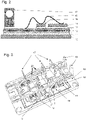
- FIG 3 shows the interior of a typical power module of Figure 1 at an intermediate stage of the assembly process without the housing.
- Insulated-Gate Bipolar Transistors (IGBT) 14 and diode chips 15 are resting on the substrates 12.
- Wire bonds 16 electrically connect the top-side of the chips with the substrates 12.
- the substrates 12 rest on a baseplate 10.
- the electrical substrate-to-substrate connection is done with individually placed sheets 21.
- Power terminals 17 are soldered to the substrates 12.
- the signal terminals 18 are connected by insulated wires 20. As can be understood, many precise operations are needed to manufacture such module.
- FIG 4 shows an assembled power module according to the present invention.
- the external power terminals 31 and signal terminals 32 are directly molded into the plastic of the housing 30.
- This housing assembly then rests as an entity on a baseplate 10.
- the power terminals 31 are supported by multiple ridges 33 as part of the housing 30 to form solid supports for the terminals 31 when contact plates are tightly screwed onto these terminals 31 by inserting screws into the screw nuts 34 positioned below the terminals 31. These screws will then brace the contact plates tightly to the terminals 31.
- FIG. 5 shows a power module according to the present invention in exploded view.
- the bottom part assembly comprises a baseplate 10, solder/sinter 42 preforms for the attachment for the substrates 12 with IGBTs, diodes, wirebonds.
- This entire bottom part is assembled by a fully automated robot and all layers are merged in a single high temperature soldering/sintering step to form a solid unit.
- a temporary fixture 43 for future alignment purposes is placed on a fresh baseplate 10.
- An automatic pick-and-place by the robot is carried out to position solder-preforms and the fully bonded substrates 12 on the baseplate 10. Subsequently, the alignment-frame 35 is put on top.
- the alignment frame 35 aligns the substrates 12 underneath during this high temperature processing, when the solder is molten, and the substrates 12 tend to "swim" on the solder/sinter 42.
- the alignment frame 35 is kept in good alignment to the baseplate 10 by a temporarily applied fixture-set 43 that is removed once forming of the solid bottom part is completed.
- top-part housing 30 assembly and the bottom part assembly are perfectly adjusted to one another and are merged in a press-in process by which the press-fit pins within the housing 30 are inserted into the respective sleeves 36, 40 in the alignment frame 35, requiring a high force in vertical direction exceeding 1 kN.
- Glue is dispensed to the housing assembly 30 prior applying the pressure.
- the housing assembly 30 is aligned to the bottom part and mounted to the baseplate 10. With a press-in force of about 40 to 150N per pin 34 at a speed of 1 to 50 mm/s this might for a high-power module result in press-in force of about 1 kN per housing assembly.
- the glue is cured and an isolation gel is applied.
- the bottom-part assembly is formed by using the alignment frame 35 to position the ceramic substrates 12 with a conductive Cu-top and bottom-side on the baseplate 10.
- These substrates 12 are attached by pre-applied solder or sinter 42 preforms at the corresponding positions of the Copper-structures incorporated in the alignment frame 35, IGBTs, diodes and wirebonds (named substrate or substrates).
- the solder/sinter 42 preforms an even and solid connection to the convexly pre-bowed baseplate 10. This pre-bow of the baseplate 10, although it is being slightly altered during the assembly process, will still be present at the final module stage to improve the thermal resistance when the module is mounted to a heat sink in application.
- the alignment frame 35 consists of a high-temperature capable plastic with incorporated Copper sheets for the electrical substrate-to-substrate connection and multiple soft Copper sleeves 36, 40 with a hardness ⁇ 60 HV.
- a critical and crucial step is the lateral positioning and the orientation of the Copper sleeves 36, 40 towards the press-fit pins 41 of the top-part housing 30 assembly and the alignment of the Copper sheets towards the substrates 12.
- This is generated by the alignment frame 35 which is formed by an assembled structure of a high temperature capable plastic with molded precisely positioned Copper sleeves 36, 40 and Copper sheets.
- this alignment frame 35 comprises downward facing pillars 38 at the outer edges and a spacer 39 ( Figure 9 ) in the center area to support precise positioning of the substrates 12 underneath.
- the spacer 39 in the center area separates the two substrates 12 from each other and sets a minimum distance, while in contrast, the downward facing pillars 38 at the outer edges restrict the maximum distance of the substrates 12.
- the alignment frame 35, substrates 12 and baseplate 10 are joined in a single high temperature >200° C solder/sintering process to each other.
- the alignment features of the alignment frame 35 keep the substrates 12 in place during the high-temperature process, when these substrates 12 tend to "swim" on the liquid solder/sinter 42 layer.
- Temporarily applied fixtures 43 mounted to the baseplate 10 guarantee the position of the alignment frame 35 with respect to the baseplate 10.
- the top-part housing assembly 30 is aligned with its press-fit pins towards the alignment frame 35 of the bottom part.
- the top-part and the bottom-part will be merged when the the top-part is pressed down to the bottom part, while the press-fit pins 41 as shown in Figure 6 penetrate the sleeves 36, 40 and form an almost uniform material and perfectly reliable electrical connection.
- the plastic housing 30 will consequently rest on the baseplate 10 and be sealed thereon with glue.
- the force in vertical direction will exceed 1 kN and requires a very solid structure that is capable to support the force applied to the top-side of the power terminals towards the press-fit pins 41 underneath.
- the Copper sleeves 36, 40 which are soldered/sintered to the substrates 12, together with the press-fit pins 41 generate the low resistance electrical connection of the external terminals towards the substrates 12.
- the Copper sheets integrated into the alignment frame 35 are also soldered/sintered to the substrates 12 and generate the low-resistance electrical connection between the substrates 12.
- the strong initial convex bow of the baseplate will be slightly reduced during the high temperature process steps. However, a certain convex final bow will remain in the final module and is desired for optimal thermal resistance when mounted on an even surface of a heat sink. The consequence is, that substrates are bent as well.
- soldering/sintering of the Copper-sleeves, incorporated in the alignment frame, to the substrates can be supported by individually adjustable distances that the sleeves are sticking out of the alignment frame. As such, these distances are anticipating the bow and therefore effectively compensate the resulting less pronounced bow.
- the electrical signal propagates from specific locations on the substrate 12 through the signal terminals 32 above the substrates. This relieves a lot of substrate 12 area otherwise needed for Copper-tracks for signal propagation and enables a high area utilization.
- Figure 6 shows the housing assembly 30 of molded terminals 31 and 32 completed by integrated screw nuts 34. Due to the ridges 33 which are a part of the housing assembly 30 and the internal supporting structure, the plastic housing 30 and the molded terminals 31 form a solid assembly which withstands high mechanical forces applied to the top-side of the power terminals. All terminals 31 and 32 have at least one or multiple downward-facing press-fit pins 41. All pins 41 are split in two legs along their longitudinal axis which form two slightly curved arches bent outward.
- Figure 7 shows a cut through the bottom part of the power module according to the present invention.
- Substrates 12 rest on the baseplate 10.
- the alignment frame structure 35 ensures precise positioning and orientation of the incorporated Copper sleeves 36 and Copper sheets (not visible in this figure). These sleeves and sheets are soldered/sintered to the substrates 12 and form a solid and complex bottom part assembly together with the baseplate 10.
- Figure 8 shows the cut through the joined top and bottom part of the power module according to the present invention after the merge.
- the press-fit pins 41 have been inserted into the sleeves 36 by a high pressing force to overcome the strong frictional forces and to ensure a perfect and durable mechanical and electrical connection.
- the arches of the two legs of the pins 41 are squeezed together.
- Figure 9 shows the cross-section of the bottom part of the power module according to the present invention.
- the alignment frame 35 is ensuring precise alignment by the pillars 38 and the spacer 39 of the substrates 12 to the alignment frame.
- Figure 10 shows an enlarged view of the area around the central metal sheet 37 incorporated in the alignment frame 35 and electrically connecting the substrates 12.
- the spacer 39 sets a minimum distance between the substrates 12.
- Figure 11 shows a top-view of the alignment frame 35 with molded Copper sleeves 36 and smaller sleeves 40. Downward facing and (hidden) the Copper sheets 37, the spacer 39 and the pillars 38.
- Figure 12 shows an alignment frame 35 with the pillars 38, the spacer 39 together with the molded Copper sheets 37, sleeves 36 and smaller sleeves 40.
- the distance of the sleeves 36 and 40 are sticking out of the alignment frame, and this sticking out can be adjusted individually to support the assembly process.
- the indicated measures of 0.94 mm, 0.97 mm or 1 mm are the measures by which the sleeves 36, 40 are sticking out of the frame. This feature is relevant to anticipate the convex bow of the baseplate 10 that is transferred to the substrates 12 and consequently results in a bent topology, which is impacting soldering/sintering and reliability. By the individually adjusted sticking out an equaling of the sleeves 36, 40 in relation to the finally less bent baseplate 10 can be reached.
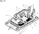
- Figure 13 shows a power module according to the present invention with the plastic housing removed, in isometric view.
- the complexly shaped power terminals 31 and signal terminals 32 with their press-fit pins 41 are joined to the individual metal sleeve 36 or 40 molded in the alignment frame 35.
- the metal structures incorporated in the alignment frame 35 are soldered/sintered to the substrates 12 which are soldered/sintered at the same process step to the baseplate 10.
- This power module can be adapted for many other technical fields. Simulations reveal a very low on-resistance which is up to a factor of two lower than competitor modules with identical outline. The internal stray inductance is also up to a factor of two lower compared to competitor modules. With the highly efficient utilization of the substrate area the world-wide highest current ratings can be achieved.
Landscapes
- Cooling Or The Like Of Semiconductors Or Solid State Devices (AREA)
- Multi-Conductor Connections (AREA)
- Coupling Device And Connection With Printed Circuit (AREA)
- Combinations Of Printed Boards (AREA)
- Inverter Devices (AREA)
Priority Applications (5)
| Application Number | Priority Date | Filing Date | Title |
|---|---|---|---|
| EP24156196.8A EP4343841A3 (de) | 2020-10-23 | 2021-06-18 | Leistungsmodul und verfahren zur herstellung desselben |
| TW110136495A TWI907532B (zh) | 2020-10-23 | 2021-09-30 | 功率模塊及其製造方法 |
| US17/508,410 US12300929B2 (en) | 2020-10-23 | 2021-10-22 | Power module and process for manufacturing the same |
| CN202111230694.4A CN114497024A (zh) | 2020-10-23 | 2021-10-22 | 功率模块及其制造方法 |
| CA3135433A CA3135433A1 (en) | 2020-10-23 | 2021-10-22 | Power module and process for manufacturing the same |
Applications Claiming Priority (1)
| Application Number | Priority Date | Filing Date | Title |
|---|---|---|---|
| EP20203681.0A EP3989274A1 (de) | 2020-10-23 | 2020-10-23 | Leistungsmodul |
Related Child Applications (2)
| Application Number | Title | Priority Date | Filing Date |
|---|---|---|---|
| EP24156196.8A Division EP4343841A3 (de) | 2020-10-23 | 2021-06-18 | Leistungsmodul und verfahren zur herstellung desselben |
| EP24156196.8A Previously-Filed-Application EP4343841A3 (de) | 2020-10-23 | 2021-06-18 | Leistungsmodul und verfahren zur herstellung desselben |
Publications (2)
| Publication Number | Publication Date |
|---|---|
| EP3989267A2 true EP3989267A2 (de) | 2022-04-27 |
| EP3989267A3 EP3989267A3 (de) | 2022-10-26 |
Family
ID=73020058
Family Applications (3)
| Application Number | Title | Priority Date | Filing Date |
|---|---|---|---|
| EP20203681.0A Withdrawn EP3989274A1 (de) | 2020-10-23 | 2020-10-23 | Leistungsmodul |
| EP24156196.8A Pending EP4343841A3 (de) | 2020-10-23 | 2021-06-18 | Leistungsmodul und verfahren zur herstellung desselben |
| EP21180413.3A Withdrawn EP3989267A3 (de) | 2020-10-23 | 2021-06-18 | Leistungsmodul und verfahren zur herstellung desselben |
Family Applications Before (2)
| Application Number | Title | Priority Date | Filing Date |
|---|---|---|---|
| EP20203681.0A Withdrawn EP3989274A1 (de) | 2020-10-23 | 2020-10-23 | Leistungsmodul |
| EP24156196.8A Pending EP4343841A3 (de) | 2020-10-23 | 2021-06-18 | Leistungsmodul und verfahren zur herstellung desselben |
Country Status (5)
| Country | Link |
|---|---|
| US (1) | US12300929B2 (de) |
| EP (3) | EP3989274A1 (de) |
| CN (1) | CN114497024A (de) |
| CA (1) | CA3135433A1 (de) |
| TW (1) | TWI907532B (de) |
Families Citing this family (7)
| Publication number | Priority date | Publication date | Assignee | Title |
|---|---|---|---|---|
| US10212838B2 (en) * | 2017-01-13 | 2019-02-19 | Cree Fayetteville, Inc. | High power multilayer module having low inductance and fast switching for paralleling power devices |
| EP3989274A1 (de) | 2020-10-23 | 2022-04-27 | SwissSEM Technologies AG | Leistungsmodul |
| JP2023176298A (ja) * | 2022-05-31 | 2023-12-13 | 富士電機株式会社 | 端子構造、端子構造の製造方法、及び半導体装置 |
| CN117954399B (zh) * | 2024-03-26 | 2024-06-25 | 淄博美林电子有限公司 | 一种高耐温度的IGBT、SiC混合功率模块 |
| KR102716013B1 (ko) * | 2024-07-09 | 2024-10-11 | 주식회사 유일로보틱스 | 외부에서 관절부 내부에 접근이 용이한 협동로봇 |
| DE102024210587A1 (de) | 2024-11-04 | 2026-05-07 | Volkswagen Aktiengesellschaft | Verfahren zur Herstellung eines elektronischen Moduls mit einem Positionierrahmen als Positionier- und Anbindungshilfe in leistungselektronischen Aufbauprozessen |
| CN121132174B (zh) * | 2025-11-18 | 2026-02-06 | 元山(济南)电子科技有限公司 | 一种高效且具备防错结构的特殊端子焊接治具 |
Family Cites Families (16)
| Publication number | Priority date | Publication date | Assignee | Title |
|---|---|---|---|---|
| EP0697728B1 (de) * | 1994-08-02 | 1999-04-21 | STMicroelectronics S.r.l. | Leistungshalbleitervorrichtung aus MOS-Technology-Chips und Gehäuseaufbau |
| JP2005142323A (ja) * | 2003-11-06 | 2005-06-02 | Mitsubishi Electric Corp | 半導体モジュール |
| US20070215997A1 (en) * | 2006-03-17 | 2007-09-20 | Martin Standing | Chip-scale package |
| US7999369B2 (en) * | 2006-08-29 | 2011-08-16 | Denso Corporation | Power electronic package having two substrates with multiple semiconductor chips and electronic components |
| US7763970B2 (en) * | 2008-02-27 | 2010-07-27 | Infineon Technologies Ag | Power module |
| DE102008012570B4 (de) * | 2008-03-04 | 2014-02-13 | Infineon Technologies Ag | Leistungshalbleitermodul-System, Leistungshalbleitermodulanordnung und Verfahren zur Herstellung einer Leistungshalbleitermodulanordnung |
| JP4576448B2 (ja) * | 2008-07-18 | 2010-11-10 | 三菱電機株式会社 | 電力用半導体装置 |
| US9041183B2 (en) * | 2011-07-19 | 2015-05-26 | Ut-Battelle, Llc | Power module packaging with double sided planar interconnection and heat exchangers |
| JP5716637B2 (ja) * | 2011-11-04 | 2015-05-13 | 住友電気工業株式会社 | 半導体モジュール及び半導体モジュールの製造方法 |
| JP2014049582A (ja) * | 2012-08-31 | 2014-03-17 | Mitsubishi Electric Corp | 半導体装置 |
| KR20150038570A (ko) * | 2012-09-14 | 2015-04-08 | 니혼 하츠쵸 가부시키가이샤 | 파워 모듈용 접속 단자 |
| WO2016185920A1 (ja) * | 2015-05-21 | 2016-11-24 | 三菱電機株式会社 | 電力用半導体装置 |
| JP2017123360A (ja) * | 2016-01-04 | 2017-07-13 | 株式会社東芝 | 半導体モジュール |
| CN111357099B (zh) * | 2017-09-15 | 2024-05-03 | 费纳模组有限公司 | 电子器件的封装方法和接合技术 |
| CN110010579B (zh) * | 2019-05-06 | 2024-03-22 | 合肥中恒微半导体有限公司 | 一种信号端子嵌入式功率半导体模块及其封装工艺 |
| EP3989274A1 (de) | 2020-10-23 | 2022-04-27 | SwissSEM Technologies AG | Leistungsmodul |
-
2020
- 2020-10-23 EP EP20203681.0A patent/EP3989274A1/de not_active Withdrawn
-
2021
- 2021-06-18 EP EP24156196.8A patent/EP4343841A3/de active Pending
- 2021-06-18 EP EP21180413.3A patent/EP3989267A3/de not_active Withdrawn
- 2021-09-30 TW TW110136495A patent/TWI907532B/zh active
- 2021-10-22 US US17/508,410 patent/US12300929B2/en active Active
- 2021-10-22 CA CA3135433A patent/CA3135433A1/en active Pending
- 2021-10-22 CN CN202111230694.4A patent/CN114497024A/zh active Pending
Also Published As
| Publication number | Publication date |
|---|---|
| EP3989267A3 (de) | 2022-10-26 |
| EP4343841A3 (de) | 2024-12-11 |
| TW202232674A (zh) | 2022-08-16 |
| EP4343841A2 (de) | 2024-03-27 |
| US20220131296A1 (en) | 2022-04-28 |
| US12300929B2 (en) | 2025-05-13 |
| CN114497024A (zh) | 2022-05-13 |
| TWI907532B (zh) | 2025-12-11 |
| CA3135433A1 (en) | 2022-03-31 |
| EP3989274A1 (de) | 2022-04-27 |
Similar Documents
| Publication | Publication Date | Title |
|---|---|---|
| US12300929B2 (en) | Power module and process for manufacturing the same | |
| CN113711351B (zh) | 具有激光焊接的引线框的功率半导体模块 | |
| JP5374831B2 (ja) | 複数の半導体チップおよび電子部品を備える2枚の基板を有するパワーエレクトロニックパッケージ | |
| CN1089493C (zh) | 功率半导体组件及其制造方法 | |
| US7986034B2 (en) | Power semiconductor module and method for producing the same | |
| WO2007130643B1 (en) | Die-on-leadframe (dol) with high voltage isolation | |
| CN108231613B (zh) | 将电子芯片与连接器主体互连并使连接器主体成形的通用过程 | |
| CN107799497A (zh) | 引线框架及其制造方法 | |
| US12519256B2 (en) | Electrical connector with meander and opening | |
| CN116960094A (zh) | 半导体器件和制造方法 | |
| CN115692355A (zh) | 具有安装在金属框架上的半导体封装的功率模块 | |
| US10957560B2 (en) | Pressure sintering procedure in which power semiconductor components with a substrate are connected to each other via a sintered connection | |
| US11557563B2 (en) | Sinter sheet, semiconductor device and manufacturing method thereof | |
| JPH11177007A (ja) | トランジスタパッケージ | |
| CN103828041A (zh) | 半导体装置 | |
| US6575765B2 (en) | Interconnect assembly for an electronic assembly and assembly method therefor | |
| CN114175223A (zh) | 功率半导体模块和形成功率半导体模块的方法 | |
| EP2688101A1 (de) | Verfahren zum elektrischen Verbinden von vertikal positionierten Substraten | |
| US12506044B2 (en) | Semiconductor device | |
| KR102724106B1 (ko) | 다층 접합 전력 모듈 및 그 제조 방법 | |
| CN119563233A (zh) | 烧结的功率电子模块 | |
| CN117121185A (zh) | 压接式半导体器件封装 | |
| CN109287130A (zh) | 电子模块、引线框以及电子模块的制造方法 | |
| CN1189938C (zh) | 无焊线式半导体装置及其封装方法 | |
| JP4822660B2 (ja) | 半導体接続用マイクロジョイント端子 |
Legal Events
| Date | Code | Title | Description |
|---|---|---|---|
| PUAI | Public reference made under article 153(3) epc to a published international application that has entered the european phase |
Free format text: ORIGINAL CODE: 0009012 |
|
| STAA | Information on the status of an ep patent application or granted ep patent |
Free format text: STATUS: THE APPLICATION HAS BEEN PUBLISHED |
|
| AK | Designated contracting states |
Kind code of ref document: A2 Designated state(s): AL AT BE BG CH CY CZ DE DK EE ES FI FR GB GR HR HU IE IS IT LI LT LU LV MC MK MT NL NO PL PT RO RS SE SI SK SM TR |
|
| RIC1 | Information provided on ipc code assigned before grant |
Ipc: H01L 25/07 20060101ALI20220413BHEP Ipc: H01L 23/04 20060101ALI20220413BHEP Ipc: H01L 23/053 20060101ALI20220413BHEP Ipc: H01L 21/50 20060101AFI20220413BHEP |
|
| RIC1 | Information provided on ipc code assigned before grant |
Ipc: H01L 25/07 20060101ALI20220811BHEP Ipc: H01L 23/04 20060101ALI20220811BHEP Ipc: H01L 23/053 20060101ALI20220811BHEP Ipc: H01L 21/50 20060101AFI20220811BHEP |
|
| RIC1 | Information provided on ipc code assigned before grant |
Ipc: H01L 25/07 20060101ALI20220818BHEP Ipc: H01L 23/04 20060101ALI20220818BHEP Ipc: H01L 23/053 20060101ALI20220818BHEP Ipc: H01L 21/50 20060101AFI20220818BHEP |
|
| PUAL | Search report despatched |
Free format text: ORIGINAL CODE: 0009013 |
|
| RIC1 | Information provided on ipc code assigned before grant |
Ipc: H01L 25/07 20060101ALI20220825BHEP Ipc: H01L 23/04 20060101ALI20220825BHEP Ipc: H01L 23/053 20060101ALI20220825BHEP Ipc: H01L 21/50 20060101AFI20220825BHEP |
|
| RIC1 | Information provided on ipc code assigned before grant |
Ipc: H01L 25/07 20060101ALI20220830BHEP Ipc: H01L 23/04 20060101ALI20220830BHEP Ipc: H01L 23/053 20060101ALI20220830BHEP Ipc: H01L 21/50 20060101AFI20220830BHEP |
|
| RIC1 | Information provided on ipc code assigned before grant |
Ipc: H01L 25/07 20060101ALI20220913BHEP Ipc: H01L 23/04 20060101ALI20220913BHEP Ipc: H01L 23/053 20060101ALI20220913BHEP Ipc: H01L 21/50 20060101AFI20220913BHEP |
|
| AK | Designated contracting states |
Kind code of ref document: A3 Designated state(s): AL AT BE BG CH CY CZ DE DK EE ES FI FR GB GR HR HU IE IS IT LI LT LU LV MC MK MT NL NO PL PT RO RS SE SI SK SM TR |
|
| STAA | Information on the status of an ep patent application or granted ep patent |
Free format text: STATUS: REQUEST FOR EXAMINATION WAS MADE |
|
| 17P | Request for examination filed |
Effective date: 20221115 |
|
| RBV | Designated contracting states (corrected) |
Designated state(s): AL AT BE BG CH CY CZ DE DK EE ES FI FR GB GR HR HU IE IS IT LI LT LU LV MC MK MT NL NO PL PT RO RS SE SI SK SM TR |
|
| STAA | Information on the status of an ep patent application or granted ep patent |
Free format text: STATUS: EXAMINATION IS IN PROGRESS |
|
| 17Q | First examination report despatched |
Effective date: 20230323 |
|
| STAA | Information on the status of an ep patent application or granted ep patent |
Free format text: STATUS: THE APPLICATION IS DEEMED TO BE WITHDRAWN |
|
| 18D | Application deemed to be withdrawn |
Effective date: 20240412 |