EP4016845A1 - Circuit d'attaque d'élément électroluminescent - Google Patents
Circuit d'attaque d'élément électroluminescent Download PDFInfo
- Publication number
- EP4016845A1 EP4016845A1 EP20882958.0A EP20882958A EP4016845A1 EP 4016845 A1 EP4016845 A1 EP 4016845A1 EP 20882958 A EP20882958 A EP 20882958A EP 4016845 A1 EP4016845 A1 EP 4016845A1
- Authority
- EP
- European Patent Office
- Prior art keywords
- current
- light
- driving circuit
- emitting
- emitting element
- Prior art date
- Legal status (The legal status is an assumption and is not a legal conclusion. Google has not performed a legal analysis and makes no representation as to the accuracy of the status listed.)
- Granted
Links
Images







Classifications
-
- H—ELECTRICITY
- H05—ELECTRIC TECHNIQUES NOT OTHERWISE PROVIDED FOR
- H05B—ELECTRIC HEATING; ELECTRIC LIGHT SOURCES NOT OTHERWISE PROVIDED FOR; CIRCUIT ARRANGEMENTS FOR ELECTRIC LIGHT SOURCES, IN GENERAL
- H05B45/00—Circuit arrangements for operating light-emitting diodes [LED]
- H05B45/30—Driver circuits
- H05B45/32—Pulse-control circuits
-
- H—ELECTRICITY
- H01—ELECTRIC ELEMENTS
- H01S—DEVICES USING THE PROCESS OF LIGHT AMPLIFICATION BY STIMULATED EMISSION OF RADIATION [LASER] TO AMPLIFY OR GENERATE LIGHT; DEVICES USING STIMULATED EMISSION OF ELECTROMAGNETIC RADIATION IN WAVE RANGES OTHER THAN OPTICAL
- H01S5/00—Semiconductor lasers
- H01S5/04—Processes or apparatus for excitation, e.g. pumping, e.g. by electron beams
- H01S5/042—Electrical excitation ; Circuits therefor
-
- G—PHYSICS
- G01—MEASURING; TESTING
- G01S—RADIO DIRECTION-FINDING; RADIO NAVIGATION; DETERMINING DISTANCE OR VELOCITY BY USE OF RADIO WAVES; LOCATING OR PRESENCE-DETECTING BY USE OF THE REFLECTION OR RERADIATION OF RADIO WAVES; ANALOGOUS ARRANGEMENTS USING OTHER WAVES
- G01S17/00—Systems using the reflection or reradiation of electromagnetic waves other than radio waves, e.g. lidar systems
-
- H—ELECTRICITY
- H03—ELECTRONIC CIRCUITRY
- H03K—PULSE TECHNIQUE
- H03K17/00—Electronic switching or gating, i.e. not by contact-making and –breaking
- H03K17/51—Electronic switching or gating, i.e. not by contact-making and –breaking characterised by the components used
- H03K17/78—Electronic switching or gating, i.e. not by contact-making and –breaking characterised by the components used using opto-electronic devices, i.e. light-emitting and photoelectric devices electrically- or optically-coupled
-
- H—ELECTRICITY
- H05—ELECTRIC TECHNIQUES NOT OTHERWISE PROVIDED FOR
- H05B—ELECTRIC HEATING; ELECTRIC LIGHT SOURCES NOT OTHERWISE PROVIDED FOR; CIRCUIT ARRANGEMENTS FOR ELECTRIC LIGHT SOURCES, IN GENERAL
- H05B45/00—Circuit arrangements for operating light-emitting diodes [LED]
- H05B45/40—Details of LED load circuits
- H05B45/44—Details of LED load circuits with an active control inside an LED matrix
- H05B45/46—Details of LED load circuits with an active control inside an LED matrix having LEDs disposed in parallel lines
-
- H—ELECTRICITY
- H05—ELECTRIC TECHNIQUES NOT OTHERWISE PROVIDED FOR
- H05B—ELECTRIC HEATING; ELECTRIC LIGHT SOURCES NOT OTHERWISE PROVIDED FOR; CIRCUIT ARRANGEMENTS FOR ELECTRIC LIGHT SOURCES, IN GENERAL
- H05B45/00—Circuit arrangements for operating light-emitting diodes [LED]
- H05B45/50—Circuit arrangements for operating light-emitting diodes [LED] responsive to malfunctions or undesirable behaviour of LEDs; responsive to LED life; Protective circuits
- H05B45/52—Circuit arrangements for operating light-emitting diodes [LED] responsive to malfunctions or undesirable behaviour of LEDs; responsive to LED life; Protective circuits in a parallel array of LEDs
-
- G—PHYSICS
- G01—MEASURING; TESTING
- G01S—RADIO DIRECTION-FINDING; RADIO NAVIGATION; DETERMINING DISTANCE OR VELOCITY BY USE OF RADIO WAVES; LOCATING OR PRESENCE-DETECTING BY USE OF THE REFLECTION OR RERADIATION OF RADIO WAVES; ANALOGOUS ARRANGEMENTS USING OTHER WAVES
- G01S7/00—Details of systems according to groups G01S13/00, G01S15/00, G01S17/00
- G01S7/48—Details of systems according to groups G01S13/00, G01S15/00, G01S17/00 of systems according to group G01S17/00
- G01S7/481—Constructional features, e.g. arrangements of optical elements
- G01S7/4814—Constructional features, e.g. arrangements of optical elements of transmitters alone
- G01S7/4815—Constructional features, e.g. arrangements of optical elements of transmitters alone using multiple transmitters
-
- H—ELECTRICITY
- H01—ELECTRIC ELEMENTS
- H01S—DEVICES USING THE PROCESS OF LIGHT AMPLIFICATION BY STIMULATED EMISSION OF RADIATION [LASER] TO AMPLIFY OR GENERATE LIGHT; DEVICES USING STIMULATED EMISSION OF ELECTROMAGNETIC RADIATION IN WAVE RANGES OTHER THAN OPTICAL
- H01S5/00—Semiconductor lasers
- H01S5/04—Processes or apparatus for excitation, e.g. pumping, e.g. by electron beams
- H01S5/042—Electrical excitation ; Circuits therefor
- H01S5/0428—Electrical excitation ; Circuits therefor for applying pulses to the laser
-
- H—ELECTRICITY
- H01—ELECTRIC ELEMENTS
- H01S—DEVICES USING THE PROCESS OF LIGHT AMPLIFICATION BY STIMULATED EMISSION OF RADIATION [LASER] TO AMPLIFY OR GENERATE LIGHT; DEVICES USING STIMULATED EMISSION OF ELECTROMAGNETIC RADIATION IN WAVE RANGES OTHER THAN OPTICAL
- H01S5/00—Semiconductor lasers
- H01S5/40—Arrangement of two or more semiconductor lasers, not provided for in groups H01S5/02 - H01S5/30
- H01S5/4025—Array arrangements, e.g. constituted by discrete laser diodes or laser bar
-
- Y—GENERAL TAGGING OF NEW TECHNOLOGICAL DEVELOPMENTS; GENERAL TAGGING OF CROSS-SECTIONAL TECHNOLOGIES SPANNING OVER SEVERAL SECTIONS OF THE IPC; TECHNICAL SUBJECTS COVERED BY FORMER USPC CROSS-REFERENCE ART COLLECTIONS [XRACs] AND DIGESTS
- Y02—TECHNOLOGIES OR APPLICATIONS FOR MITIGATION OR ADAPTATION AGAINST CLIMATE CHANGE
- Y02B—CLIMATE CHANGE MITIGATION TECHNOLOGIES RELATED TO BUILDINGS, e.g. HOUSING, HOUSE APPLIANCES OR RELATED END-USER APPLICATIONS
- Y02B20/00—Energy efficient lighting technologies, e.g. halogen lamps or gas discharge lamps
- Y02B20/30—Semiconductor lamps, e.g. solid state lamps [SSL] light emitting diodes [LED] or organic LED [OLED]
Definitions
- the present disclosure relates to a light-emitting element driving circuit.
- Patent Document 1 discloses a technique related to a current generation circuit for an array element.
- This circuit includes one reference voltage input and transistors each a constituting constant current generation circuit for an associated channel.
- the reference voltage input is connected to respective bases of the transistors via passive circuitry.
- the respective emitters of the transistors are connected to a common ground line via resistors.
- the respective constant current generation circuits in the channels are intensively disposed in a specific region on an integrated circuit chip.
- the respective collector output currents of the transistors are individually supplied to array functional circuit blocks distributed in the integrated circuit chip.
- Patent Document 2 discloses a technique related to a light source device of an optical head.
- the device includes a common package, a single-mode oscillating semiconductor laser and a multi-mode oscillating semiconductor laser incorporated in the package, and a high-frequency oscillation circuit.
- the high-frequency oscillation circuit generates a high-frequency current to be superimposed on a driving current of the semiconductor laser in order to convert the single-mode oscillating semiconductor laser into multi-mode oscillation.
- This device has means for preventing unnecessary radiation due to a high-frequency current.
- This means includes a high-frequency component absorber circuit provided in a feed line of the multi-mode oscillating semiconductor laser.
- the high-frequency component absorber circuit is a band pass filter, a choke coil, or a ferrite bead.
- the inventors have found a problem described below. That is, when a plurality of semiconductor light-emitting elements are individually driven, independent driving circuit units are usually used for the associated semiconductor light-emitting elements.
- the cathodes may be set to the same potential (a configuration in which the respective cathodes of the semiconductor light-emitting elements are connected to a common line).
- the plurality of driving circuit units are short-circuited to each other via the common line.
- the semiconductor light-emitting elements are individually driven, it is necessary to arrange a contrivance to prevent the driving current from flowing to the other semiconductor light-emitting elements via the common line.
- the present disclosure has been made to solve the above-described problems, and an object of the present disclosure is to provide a light-emitting element driving circuit having a structure for individually pulse-driving a plurality of semiconductor light-emitting elements each having a cathode, the cathodes of the plurality of semiconductor light-emitting elements being electrically connected to each other via a common line.
- a light-emitting element driving circuit is a circuit configured to individually perform drive control of a plurality of semiconductor light-emitting elements, and includes a plurality of driving circuit units associated one-to-one with the plurality of semiconductor light-emitting elements.
- the cathodes of the plurality of semiconductor light-emitting elements may be unified as a cathode electrode by a monolithic structure, or may be electrically connected via a common line and/or a common terminal. As a result, the cathodes of the plurality of semiconductor light-emitting elements are set to the same potential.
- the plurality of driving circuit units individually pulse-drives the associated semiconductor light-emitting elements.
- Each of the plurality of driving circuit units includes a current control element, a first energy storage element, and a switching device.
- the current control element has a first terminal electrically connected to the cathode of the associated semiconductor light-emitting element via a first node, and a second terminal electrically connected to an anode of the associated semiconductor light-emitting element via a second node.
- the current control element causes current to flow from the first node to the second node while the associated semiconductor light-emitting element is in the non-light-emitting state, and limits the current while the associated semiconductor light-emitting element is in the light-emitting state.
- the first energy storage element includes a first electrode electrically connected to the first node and a second electrode.
- the switching element includes a control terminal to which a control signal for driving the associated semiconductor light-emitting element is inputted, a first current terminal electrically connected to the second electrode of the first energy storage element, and a second current terminal electrically connected to the second node.
- each of second electrodes of the first energy storage elements in the plurality of driving circuit units is electrically connected to a first constant potential line.
- Each of second nodes in the plurality of driving circuit units is electrically connected to a second constant potential line via a first current interrupting element or directly.
- the first current interrupting element is disposed on the line between two adjacent second nodes and avoids a short circuit between the two adjacent second nodes.
- the second constant potential line is set to a lower potential than the first constant potential line.
- the control target of the first current interrupting element is at least a current with a specific frequency or a current in a specific period.
- the first current interrupting element interrupts or suppresses the control target.
- the first current interrupting element interrupts or suppresses current at least during a period in which the switching element is in an ON-state.
- each of second electrodes of the first energy storage elements in the plurality of driving circuit units is electrically connected to a first constant potential line.
- Each of second nodes in the plurality of driving circuit units is electrically connected to a second constant potential line via a first current interrupting element or directly.
- the first current interrupting element is disposed on the line between two adjacent second nodes and avoids a short circuit between the two adjacent second nodes.
- the second constant potential line is set to a lower potential than the first constant potential line.
- the control target of the first current interrupting element is at least a current with a specific frequency or a current in a specific period.
- the first current interrupting element interrupts or suppresses the control target.
- the first current interrupting element interrupts or suppresses current at least during a period in which the switching element is in an ON-state.
- the first electrode is electrically connected to the first node, and the second electrode is electrically connected to a first constant potential line (for example, positive power supply line).
- a current control element is connected to the first node, and the current control element causes a current to flow from the first node to the second node when the semiconductor light-emitting element does not emit light.
- the second node is electrically connected to a second constant potential line (for example, a ground line) having a potential lower than that of the first constant potential line.
- the charge accumulated in the first energy storage element of the driving circuit unit returns from the second electrode of the first energy storage element to the first electrode of the first energy storage element through the second node, the semiconductor light-emitting element, and the first node.
- the semiconductor light-emitting element corresponding to the driving circuit unit on a one-to-one basis emits light (is driven).
- the current control element limits the current, the charge can flow to the semiconductor light-emitting element without bypassing.
- the first current interrupting element is not provided, a part of the charge flows from the second node to the second node of another driving circuit unit, and return to the first energy storage element of the driving circuit unit through the semiconductor light-emitting element of the other driving circuit unit and the cathode of the semiconductor device.
- the semiconductor light-emitting element of the other driving circuit unit also emits light, and individual driving of the semiconductor light-emitting elements cannot be realized.
- the first current interrupting element is interposed between two adjacent second nodes among the second nodes in the plurality of driving circuit units, and the two adjacent second nodes are not short-circuited.
- each of the plurality of driving circuit units may further include a second current interrupting element arranged on the line between the first constant potential line and the second electrode of the first energy storage element.
- the control target of the second current interrupting element is at least a current with a specific frequency or a current in a specific period.
- the second current interrupting element is an element that interrupts or suppresses the control target.
- the second current interrupting element interrupts or suppresses a current at least during a period in which the switching element is in an ON-state.
- the current is prevented from flowing from the first constant potential line to the second node through the switching element during the period in which the switching element is in the ON-state (the increase in the potential of the second node can be suppressed).
- a potential difference in one example, a gate-source voltage of the FET
- each of the plurality of driving circuit units may further include a second energy storage element having a first electrode electrically connected to a third node between the second electrode of the first energy storage element and the second current interrupting element, and a first electrode electrically connected to the second node.
- a current is supplied from the first constant potential line to the second energy storage element of each of the driving circuit units, and a charge is accumulated in the second energy storage element.
- the first energy storage element can be instantaneously recharged with the charge accumulated in the second energy storage element regardless of the interruption or suppression of the current by the second current interrupting element.
- the capacity of the second energy storage element is preferably larger than the capacity of the first energy storage element.
- the first energy storage element can be recharged every emission of light regardless of the interruption or suppression of the current by the second current interrupting element.
- the first current interrupting element may include an inductor.
- the inductor functions as a low pass filter, and can interrupt or suppress a high frequency current in pulse driving. Therefore, it is possible to interrupt or suppress the current passing through when the switching element is turned on.
- the current control element may include a resistance element.
- the impedance of the current control element since the impedance of the current control element is higher than the forward impedance of the semiconductor light-emitting element, a current can be limited when the semiconductor light-emitting element emits light.
- the impedance of the current control element since the impedance of the current control element is lower than the impedance in the reverse direction of the semiconductor light-emitting element, a current can flow when the semiconductor light-emitting element does not emit light.
- the plurality of driving circuit units may individually drive the plurality of semiconductor light-emitting elements integrated on a common semiconductor substrate.
- a semiconductor layer including an active layer is provided on the semiconductor substrate, and a cathode electrode serving as a common cathode of the plurality of semiconductor light-emitting elements is provided on a back surface of the semiconductor layer.
- a plurality of anode electrodes corresponding to the anodes of the plurality of semiconductor light-emitting elements are provided on the upper surface of the semiconductor layer.
- cathodes (cathode electrodes) of the plurality of semiconductor light-emitting elements may be electrically connected via a common line and/or a common terminal. Both of the configurations can reduce the size of the semiconductor substrate and contribute to downsizing of the light-emitting device.
- Fig. 1 is a circuit diagram illustrating a configuration of a light-emitting element driving circuit 1 according to an embodiment of the present disclosure.
- the light-emitting element driving circuit 1 includes a plurality of driving circuit units 2A to 2D.
- the driving circuit units 2A to 2D is a circuit that individually pulse-drive a plurality of semiconductor light-emitting elements 4 (hereinafter, simply referred to as light-emitting elements 4) having cathodes set to the same potential.
- light-emitting elements 4 are, for example, laser diodes.
- the output wavelengths of the light-emitting elements 4 are included, for example, in the near-infrared range.
- the peak oscillation wavelength of each of the light-emitting element 4 is 905 nm, and the peak output of each of the light-emitting element 4 is, for example, 100 W.
- a semiconductor light-emitting element array suitable for light detection and ranging (LiDAR) can be provided.
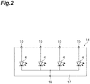
- Fig. 2 is a schematic plan view of a semiconductor light-emitting element array 14.
- the semiconductor light-emitting element array 14 has a monolithic structure in which the plurality of light-emitting elements 4 is integrated on a common semiconductor substrate 17. If the output wavelength is in the near-infrared range, the material of the semiconductor substrate 17 is, for example, GaAs or InP, and the material of the semiconductor layer provided on the semiconductor substrate 17 and including an active layer is, for example, AlGaAs, InGaAs, or InGaAsP.
- a cathode electrode (common cathode) used in common as cathodes of the plurality of light-emitting elements 4 is provided on a back surface of the semiconductor layer, and a plurality of anode electrodes separated from each other corresponding to anodes of the plurality of light-emitting elements 4 is provided on an upper surface of the semiconductor layer.
- the semiconductor light-emitting element array 14 includes a plurality of anode terminals 15 connected to the plurality of anode electrodes, and one cathode terminal 16 connected to the common cathode electrode.
- each of the driving circuit units 2A to 2D has the same circuit configuration.
- Each of the driving circuit units 2A to 2D includes a transistor 3 (switching element), a capacitor 5 (first energy storage element), a current control element 6, a capacitor 7 (second energy storage element), a current interrupting element 8 (first current interrupting element), a current interrupting element 9 (second current interrupting element), and a resistance element 13.
- the transistor 3 is an example of a switching element in the present embodiment, and is a selection unit for individually driving the light-emitting elements 4.
- the transistor 3 is, for example, a field effect transistor (FET).
- FET field effect transistor
- the transistor 3 is not limited to an FET, and may be, for example, a bipolar transistor.
- the transistor 3 has a control terminal and a pair of current terminals. If the transistor 3 is an FET, the control terminal is a gate, and the pair of current terminals is a source and a drain. If the transistor 3 is a bipolar transistor, the control terminal is a base, and the pair of current terminals is a collector and an emitter.
- Fig. 1 clearly illustrates parasitic diodes 12 included in the transistors 3.
- the current control element 6 is connected in parallel with the light-emitting element 4 driven by a driving circuit to which the current control element 6 belongs. Specifically, the current control element 6 and the light-emitting element 4 are connected in parallel between a cathode-side node N 1 (first node) and an anode-side node N 2 (second node) of the light-emitting element 4.
- the current control element 6 causes a current to flow from the node N 1 to the node N 2 during the non-light emission period of the light-emitting element 4, and limits a current from the node N 2 to the node N 1 during the light emission period of the light-emitting element 4.
- the current interrupting element 9 can include these electronic components individually or in combination.
- Fig. 1 illustrates a circuit including only inductors as the current interrupting elements 9. In that case, the current interrupting elements 9 function as low-pass filters. If the current interrupting elements 8 and 9 are low-pass filters, their cutoff frequencies may be equal to each other or different from each other. If the current interrupting elements 8 and 9 are both inductors, their inductances may be equal to each other or different from each other.
- the capacitor 7 is, for example, a chip capacitor mounted on a circuit board.
- the capacitor 7 has a pair of electrodes and accumulates a charge between the pair of electrodes.
- the capacitance value of the capacitor 7 is larger than the capacitance value of the capacitor 5, and is, for example, 0.1 ⁇ F or more. In other words, the capacitance value of the capacitor 7 is, for example, 100 times or more the capacitance value of the capacitor 5.
- One electrode of the capacitor 7 is electrically connected to the node N 3 (third node).
- the node N 3 is a node between the electrode of the capacitor 5 on the power supply line 10 side and the current interrupting element 9 (in the present embodiment, between the resistance element 13 and the current interrupting element 9).
- the other electrode of the capacitor 7 is electrically connected to the node N 2 .
- one electrode of the capacitor 5 is electrically connected to the node N 1 , and the other electrode of the same is electrically connected to the power supply line 10. Further, the current control element 6 is connected to the node N 1 , and the current control element 6 causes current to flow from the node N 1 to the node N 2 when the light-emitting element 4 does not emit light.
- the node N 2 is electrically connected to the reference potential line 11 having a potential lower than that of the power supply line 10.
- the current Ia is supplied from the power supply line 10 to the capacitors 5 of the driving circuit units 2A to 2D, and charges are accumulated in the capacitors 5 as illustrated in Fig. 3 .
- the driving circuit unit 2A the driving circuit unit 2A will be taken in the description
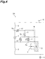
- the charge accumulated in the capacitor 5 of the driving circuit unit 2A instantaneously flows as the driving current Ib from the electrode of the capacitor 5 on the power supply line 10 side through the transistor 3, the node N 2 , the light-emitting element 4, and the node N 1 , and returns to the electrode of the capacitor 5 on the opposite side as illustrated in Fig. 4 .
- the light-emitting element 4 of the driving circuit unit 2A is pulse-driven to emit light.
- the current control element 6 limits the current, the driving current Ib can flow to the light-emitting element 4 without bypassing.
- the resistance element 13 inhibits the charge accumulated in the capacitor 7 from flowing to the transistor 3. Note that similar operation is possible in any of the driving circuit units 2B, 2C, and 2D.
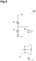
- Fig. 5 is a circuit diagram illustrating a configuration of a driving circuit 20A according to a first comparative example.
- the driving circuit 20A is a circuit for driving a single light-emitting element 4A, and includes a transistor 21 connected in series between a cathode of the light-emitting element 4A and the reference potential line 11, and a resistance element 23 and a capacitor 22 connected in series between the power supply line 10 and the reference potential line 11 and connected in series with each other.
- An anode of the light-emitting element 4 is connected to a node between the resistance element 23 and the capacitor 22.
- the driving circuit 20A In the driving circuit 20A, during a period in which the transistor 21 is in the OFF-state, current from the power supply line 10 is supplied to the capacitor 22, and a charge is accumulated in the capacitor 22. Then, when the transistor 21 is turned on, the charge accumulated in the capacitor 22 instantaneously flow to the reference potential line 11 through the light-emitting element 4A and the transistor 21. Thus, the light-emitting element 4A is pulse-driven to emit light.
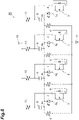
- Fig. 6 is a circuit diagram illustrating a configuration of a driving circuit 20B according to a second comparative example for driving four light-emitting elements 4 each having a cathode, the four cathodes being electrically connected to each other via a common line.
- the driving circuit 20B includes respective resistance elements 23 and capacitors 22 provided for the light-emitting elements 4, and a transistor 21 provided in common for the four light-emitting elements 4.
- a connection aspect between the light-emitting elements 4 and the resistance elements 23 and the capacitors 22 is similar to that in Fig. 5 .
- the transistor 21 is connected in series between the common cathode of the four light-emitting elements 4 and the reference potential line 11.
- the power supply line 10 is in common for the light-emitting elements 4.
- the driving circuit 20B In the driving circuit 20B, during a period in which the transistor 21 is in the OFF-state, current from the power supply line 10 is supplied to the capacitors 22, and charges are accumulated in the capacitors 22. Then, when the transistor 21 is turned on, the charges accumulated in the capacitors 22 instantaneously flow to the reference potential line 11 through the light-emitting elements 4A and the transistors 21. Thus, the four light-emitting elements 4A are concurrently pulse-driven to emit light. Therefore, the four light-emitting elements 4 cannot be individually driven in the driving circuit 20B.
- Fig. 7 is a circuit diagram illustrating a driving circuit 20C according to an improved third comparative example.
- the driving circuit 20C further includes four transistors 24, four transistors 25, and a resistance element 26 in addition to the composition of the driving circuit 20B illustrated in Fig. 6 .
- the transistors 24 and 25 constitute switching circuits provided for each of the light-emitting elements 4.
- the transistor 24 is connected in series between the common power supply line 10 and the capacitor 22 and the light-emitting element 4, and controls current supplied to the capacitor 22.
- the transistor 25 constitutes a series circuit with the resistance element 27, and one end of the series circuit on the resistance element 27 side is connected to the power supply line 10 and the other end of the same is connected to the reference potential line 11.
- a node between the transistor 25 and the resistance element 27 is connected to a control terminal of the transistor 24, and a potential (driving control signal) of the node is applied to the control terminal of the transistor 24. That is, the transistor 25 is switched between ON- and OFF-states corresponding to ON- and OFF-states of the transistor 24.
- the transistors 24 are, for example, p-channel MOSFETs, and the transistors 25 are, for example, n-channel MOSFETs. According to this configuration, a high-withstand-voltage switching circuit can be constituted.
- the resistance element 26 is connected in series between the four capacitors 22 and the common reference potential line 11.
- the driving circuit 20C first, in order to accumulate charges in the capacitor 22 corresponding to the light-emitting element 4 to be caused to emit light, the transistor 25 corresponding to the light-emitting element 4 is turned on. Accordingly, the transistor 24 corresponding to the light-emitting element 4 is turned on, and charges are accumulated in the capacitor 22. Thereafter, when the transistor 21 is turned on, current is instantaneously supplied from the capacitor 22 to the light-emitting element 4, and the light-emitting element 4 is pulse-driven to emit light.
- this driving circuit 20C has a problem described below. That is, when a charge is accumulated in the capacitor 22 corresponding to the light-emitting element 4 to be caused to emit light, the voltage between both ends of the capacitor 22 increases. During the period in which the transistor 21 is in the OFF-state, this voltage between the both ends is applied as a reverse bias to the cathodes of the other three light-emitting elements 4 via the light-emitting element 4, and a reverse current having a magnitude proportional to this reverse bias flows through the light-emitting elements 4 and is supplied to the other three capacitors 22. As a result, charges are also accumulated in the other three capacitors 22.
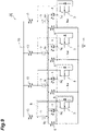
- Fig. 8 is a circuit diagram illustrating a driving circuit 30 according to a fourth comparative example.
- the driving circuit 30 includes respective transistors 3, capacitors 5, and current control elements 6 provided for light-emitting elements 4. Note that the interconnection relationship among the transistors 3, the capacitors 5, and the current control elements 6 is similar to that of the present embodiment illustrated in Fig. 1 .
- the electrode of each of the capacitors 5 on the power supply line 10 side is connected to a common power supply line 10 via only a resistance element 13, and a node N 2 is short-circuited to a reference potential line 11.
- capacitors 7 are not provided.
- the driving circuit 30 during a period in which the transistors 3 are in an OFF-state (that is, during a non-light emitting period of the light-emitting elements 4), current is supplied from the power supply line 10 to the capacitors 5 and charges are accumulated in the capacitors 5. Then, when a certain transistor 3 (for example, the left-end transistor 3) is turned on, the charge accumulated in the capacitor 5 connected to the transistor 3 instantaneously flows as a driving current Ib through the transistor 3, the node N 2 , the light-emitting element 4, and a node N 1 , and returns to the capacitor 5 as illustrated in Fig. 9 . Thus, the light-emitting element 4A is pulse-driven to emit light. At this time, since the current control element 6 limits the current, the driving current Ib can flow to the light-emitting element 4 without bypassing.
- the driving current Ib can flow to the light-emitting element 4 without bypassing.
- a part Iba of the driving current Ib flows from the node N 2 to the node N 2 of another light-emitting element 4, and returns to the original capacitor 5 through the other light-emitting element 4 and the common cathode.
- the other light-emitting element 4 also emits light, and thus individual driving of the light-emitting elements 4 cannot be realized.
- the current interrupting elements 8 are interposed between the nodes N 2 of the driving circuit units 2A to 2D, and the nodes N 2 of the driving circuit units 2A to 2D are not short-circuited to each other.
- the current interrupting element 8 is an element that interrupts or suppresses a current at least with a specific frequency or in a specific period, and interrupts or suppresses the current at least in a period during which the transistor 3 is in the ON-state.
- the capacitor 5 can be instantaneously recharged with the charge accumulated in the capacitor 7 regardless of the interruption or suppression of the current by the current interrupting element 9. Therefore, the light-emitting element 4 can be caused to emit light again in a short time, thereby allowing high-speed driving of the light-emitting elements 4.
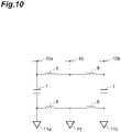
- Fig. 10 is a circuit diagram conceptually illustrating a power supply system included in the light-emitting element driving circuit 1 in the present embodiment.
- Fig. 10 illustrates respective capacitors 7, inductors as the current interrupting elements 8, and inductors as the current interrupting elements 9 of the two driving circuit units 2A and 2B among the driving circuit units 2A to 2D.
- Fig. 10 also illustrates the common power supply line 10 and the common reference potential line 11.
- a filter circuit is constituted by the plurality of inductors constituting the current interrupting elements 8 and 9, and respective power supply systems of the driving circuit units 2A and 2B are virtually separated from each other by the filter circuit.
- Fig. 10 is a circuit diagram conceptually illustrating a power supply system included in the light-emitting element driving circuit 1 in the present embodiment.
- Fig. 10 illustrates respective capacitors 7, inductors as the current interrupting elements 8, and inductors as the current interrupting elements 9 of the two driving circuit units 2A and 2B among the driving circuit units 2A to
- FIG. 10 illustrates a virtual power supply line 10a and a reference potential line 11a that supply a power supply voltage to the driving circuit unit 2A, and a virtual power supply line 10b and a reference potential line 11b that supply a power supply voltage to the driving circuit unit 2B.
- the current (graph G2) of the other light-emitting element 4 does not change at all, and the pulse driving current Ib is hardly supplied to the other light-emitting element 4. That is, according to the light-emitting element driving circuit 1 of the present embodiment, the ratio (Pb/Pa) between a light output Pa of the light-emitting element 4 that is caused to emit light and a light output Pb of the light-emitting element 4 that is not caused to emit light can be made extremely small.
- the current interrupting element 8 may include an inductor.
- the inductor functions as a low pass filter, and can interrupt or suppress a high frequency current in pulse driving. Therefore, it is possible to interrupt or suppress the current from passing during the period in which the transistor 3 is in the ON-state.
- the current control element 6 may include a resistance element.
- the impedance of the current control element 6 since the impedance of the current control element 6 is higher than the forward impedance of the light-emitting element 4, current can be limited during the light emission period of the light-emitting element 4.
- the impedance of the current control element 6 since the impedance of the current control element 6 is lower than the reverse impedance of the light-emitting element 4, current can flow during the non-light emission period of the light-emitting element 4. This makes it easy to realize the current control element 6 that causes current to flow from the node N 1 to the node N 2 during the non-light emission period of the light-emitting element 4 and limits the current during the light emission period of the light-emitting element 4.
- appropriately selecting the resistance value of the resistance element (more preferably, together with the resistance value of the resistance element 13) makes it possible to control the speed at which a charge is accumulated in the capacitor 5.
- the plurality of light-emitting elements 4 may be integrated on a common semiconductor substrate 17.
- unifying the cathodes of the plurality of light-emitting elements 4 (using one cathode electrode as the cathodes of the plurality of light-emitting elements 4) can downsize the semiconductor substrate 17, thereby contributing to miniaturization of the light-emitting device.
- Fig. 14 is a circuit diagram illustrating a light-emitting element driving circuit 1A according to a modification example of the above embodiment.
- a node N 2 of one of driving circuit units 2A to 2D (for example, the driving circuit unit 2D) is electrically connected directly (with substantially zero resistance) to a reference potential line 11 without a current interrupting element 8.
- the nodes N 2 of the driving circuit units 2A to 2D are connected via the current interrupting elements 8 without short-circuiting each other.
- the node N 2 of the driving circuit unit 2C is electrically connected to the reference potential line 11 via one current interrupting element 8
- the node N 2 of the driving circuit unit 2B is electrically connected to the reference potential line 11 via two current interrupting elements 8
- the node N 2 of the driving circuit unit 2A is electrically connected to the reference potential line 11 via three current interrupting elements 8.
- connection aspect between the nodes N 2 of the driving circuit units 2A to 2D and the reference potential line 11 is not limited to the aspect illustrated in Fig. 1 , and may be, for example, a aspect as in the present modification.
- the nodes N 2 of the driving circuit units 2A to 2D are connected to each other via the current interrupting elements 8 without short-circuiting each other, and are electrically connected to the reference potential line 11 via the current interrupting elements 8 or directly, so that the same advantageous effects as those of the above embodiment can be obtained.
- Fig. 1 illustrates inductors as filters constituting the current interrupting elements 8 and 9.
- filters constituting the current interrupting elements 8 and 9 for example, various other elements such as chip ferrite beads and RC filter circuits can be applied as long as they are low-pass filters or band-pass filters that interrupt or suppress an AC current of high frequencies (for example, GHz band) in pulse driving and pass a current of low frequencies (for example, DC to kHz band).
- the chip ferrite bead can be formed in a single chip for each driving circuit, so that the light-emitting element driving circuit 1 can be easily configured.
- At least one of the current interrupting elements 8 and 9 is not necessarily a filter.
- the current interrupting elements 8 and 9 illustrated in Fig. 1 may include resistance elements instead of inductors (or in addition to inductors) as elements for interrupting or suppressing at least a current with a specific frequency.
- the current interrupting elements 8 and 9 may be constituted only by the resistance elements.
- one end of the resistance element as the current interrupting element 8 is electrically connected to the node N 2 , and the other end of the same is electrically connected to the reference potential line 11.
- the other electrode of the capacitor 5 is electrically connected to the power supply line 10 via a resistance element as the current interrupting element 9.
- At least one of the current interrupting elements 8 and 9 in Fig. 1 may include a switching element such as a transistor instead of the inductor (or in addition to the inductor) as an element for interrupting or suppressing a current in at least a specific period.
- the switching element may be turned off during a certain period including the period in which the transistor 3 is in the ON-state (that is, the light emission period of the light-emitting element 4), and the switching element may be turned on during other periods.
- the same advantageous effects as those of the above embodiment can be obtained.
- switching elements as many as the number of driving circuits, a control circuit for driving these switching elements, and the like are further required.
- the current interrupting elements 8 and 9 are constituted by filters, a control circuit is not required, and the current interrupting elements 8 and 9 can be constituted at a lower cost than the switching elements, which is advantageous in terms of reduction in manufacturing cost and downsizing of the device.
- Fig. 1 illustrates a case where each of the driving circuit units 2A to 2D drives one light-emitting element 4, each of the driving circuit units 2A to 2D may drive two or more light-emitting elements 4.
- the number of the light-emitting elements 4 may be larger than the number of the driving circuit units 2A to 2D.
- each of the light-emitting elements 4 illustrated in Fig. 1 is replaced with two or more light-emitting elements 4 connected in parallel or in series with each other.
Landscapes
- Physics & Mathematics (AREA)
- General Physics & Mathematics (AREA)
- Electromagnetism (AREA)
- Engineering & Computer Science (AREA)
- Condensed Matter Physics & Semiconductors (AREA)
- Optics & Photonics (AREA)
- Computer Networks & Wireless Communication (AREA)
- Radar, Positioning & Navigation (AREA)
- Remote Sensing (AREA)
- Led Devices (AREA)
- Semiconductor Lasers (AREA)
- Electronic Switches (AREA)
Applications Claiming Priority (2)
| Application Number | Priority Date | Filing Date | Title |
|---|---|---|---|
| JP2019198559A JP7428500B2 (ja) | 2019-10-31 | 2019-10-31 | 発光素子駆動回路 |
| PCT/JP2020/039685 WO2021085292A1 (fr) | 2019-10-31 | 2020-10-22 | Circuit d'attaque d'élément électroluminescent |
Publications (3)
| Publication Number | Publication Date |
|---|---|
| EP4016845A1 true EP4016845A1 (fr) | 2022-06-22 |
| EP4016845A4 EP4016845A4 (fr) | 2023-07-26 |
| EP4016845B1 EP4016845B1 (fr) | 2025-04-02 |
Family
ID=75713547
Family Applications (1)
| Application Number | Title | Priority Date | Filing Date |
|---|---|---|---|
| EP20882958.0A Active EP4016845B1 (fr) | 2019-10-31 | 2020-10-22 | Circuit d'attaque d'élément électroluminescent |
Country Status (6)
| Country | Link |
|---|---|
| US (1) | US11729885B2 (fr) |
| EP (1) | EP4016845B1 (fr) |
| JP (1) | JP7428500B2 (fr) |
| KR (1) | KR102837771B1 (fr) |
| CN (1) | CN114616733B (fr) |
| WO (1) | WO2021085292A1 (fr) |
Families Citing this family (7)
| Publication number | Priority date | Publication date | Assignee | Title |
|---|---|---|---|---|
| WO2022127073A1 (fr) * | 2020-12-18 | 2022-06-23 | 青岛海信宽带多媒体技术有限公司 | Module optique |
| JP1701619S (fr) | 2021-01-20 | 2021-12-06 | ||
| JP1712335S (ja) | 2021-01-20 | 2022-04-12 | 発光素子モジュール | |
| USD1089808S1 (en) | 2021-01-20 | 2025-08-19 | Hamamatsu Photonics K.K. | Light-emitting element module |
| USD1083850S1 (en) * | 2021-01-20 | 2025-07-15 | Hamamatsu Photonics K.K. | Light-emitting element module |
| JP1701505S (fr) | 2021-01-20 | 2021-12-06 | ||
| US20250112440A1 (en) * | 2023-09-28 | 2025-04-03 | Lawrence Livermore National Security, Llc | Photoconductive switch laser diode driver |
Family Cites Families (19)
| Publication number | Priority date | Publication date | Assignee | Title |
|---|---|---|---|---|
| JPS51147983A (en) | 1975-06-14 | 1976-12-18 | Fujitsu Ltd | Driving circuit for light emission diode |
| JP3313571B2 (ja) | 1996-03-29 | 2002-08-12 | 株式会社東芝 | アレイ素子用電流発生回路 |
| JP4123791B2 (ja) | 2001-03-05 | 2008-07-23 | 富士ゼロックス株式会社 | 発光素子駆動装置および発光素子駆動システム |
| JP2002288864A (ja) | 2001-03-28 | 2002-10-04 | Sankyo Seiki Mfg Co Ltd | 光ヘッドの光源装置 |
| JP3988469B2 (ja) * | 2002-01-25 | 2007-10-10 | ソニー株式会社 | 半導体レーザ駆動回路 |
| JP4683964B2 (ja) | 2004-04-28 | 2011-05-18 | ルネサスエレクトロニクス株式会社 | レーザーダイオードの駆動回路及び半導体装置 |
| US7995012B2 (en) * | 2005-12-27 | 2011-08-09 | Semiconductor Energy Laboratory Co., Ltd. | Light emitting device |
| US20090187925A1 (en) | 2008-01-17 | 2009-07-23 | Delta Electronic Inc. | Driver that efficiently regulates current in a plurality of LED strings |
| JP4614189B2 (ja) | 2008-05-12 | 2011-01-19 | 株式会社デンソー | 燃料噴射装置 |
| JP2011199220A (ja) | 2010-03-24 | 2011-10-06 | Sharp Corp | 発光素子駆動装置 |
| DE102010041632A1 (de) | 2010-09-29 | 2012-03-29 | Osram Gesellschaft mit beschränkter Haftung | Schaltungsanordnung zum Betreiben mindestens zweier Halbleiterlichtquellen |
| JP6030922B2 (ja) * | 2012-06-11 | 2016-11-24 | 株式会社小糸製作所 | 光源制御装置 |
| KR20150141396A (ko) | 2014-06-10 | 2015-12-18 | 김경일 | 잔상을 제거할 수 있는 led 모듈 |
| US10097908B2 (en) | 2014-12-31 | 2018-10-09 | Macom Technology Solutions Holdings, Inc. | DC-coupled laser driver with AC-coupled termination element |
| KR102290399B1 (ko) * | 2015-03-04 | 2021-08-24 | 주식회사 디비하이텍 | 발광 소자 구동 장치 |
| US10158211B2 (en) | 2015-09-22 | 2018-12-18 | Analog Devices, Inc. | Pulsed laser diode driver |
| US10574026B2 (en) | 2017-03-23 | 2020-02-25 | Infineon Technologies Ag | Circuit and method for driving a laser diode |
| JP2019068528A (ja) | 2017-09-28 | 2019-04-25 | 株式会社リコー | 昇圧回路、電源回路、光源駆動回路及び距離計測装置 |
| JP2019135740A (ja) | 2018-02-05 | 2019-08-15 | 住友電気工業株式会社 | レーザ駆動回路及び光送信器 |
-
2019
- 2019-10-31 JP JP2019198559A patent/JP7428500B2/ja active Active
-
2020
- 2020-10-22 US US17/637,487 patent/US11729885B2/en active Active
- 2020-10-22 WO PCT/JP2020/039685 patent/WO2021085292A1/fr not_active Ceased
- 2020-10-22 KR KR1020227007840A patent/KR102837771B1/ko active Active
- 2020-10-22 CN CN202080075716.1A patent/CN114616733B/zh active Active
- 2020-10-22 EP EP20882958.0A patent/EP4016845B1/fr active Active
Also Published As
| Publication number | Publication date |
|---|---|
| JP2021072377A (ja) | 2021-05-06 |
| CN114616733A (zh) | 2022-06-10 |
| US20220279638A1 (en) | 2022-09-01 |
| EP4016845B1 (fr) | 2025-04-02 |
| EP4016845A4 (fr) | 2023-07-26 |
| CN114616733B (zh) | 2025-02-18 |
| US11729885B2 (en) | 2023-08-15 |
| WO2021085292A1 (fr) | 2021-05-06 |
| KR102837771B1 (ko) | 2025-07-24 |
| KR20220092854A (ko) | 2022-07-04 |
| JP7428500B2 (ja) | 2024-02-06 |
Similar Documents
| Publication | Publication Date | Title |
|---|---|---|
| US11729885B2 (en) | Light-emitting element driving circuit | |
| US6292500B1 (en) | Semiconductor laser device | |
| JP6839280B2 (ja) | GaNトランジスタに基づく電力コンバータのためのブートストラップキャパシタ過電圧管理回路 | |
| US11990838B2 (en) | Driver circuit and method for providing a pulse | |
| US8222838B2 (en) | Light-emitting-element driving circuit | |
| US20220376472A1 (en) | Laser diode driver circuit | |
| US12010774B2 (en) | PWM controlled power source and method | |
| WO2021079611A1 (fr) | Circuit d'attaque de diode laser | |
| US12327982B2 (en) | Laser diode drive circuit | |
| US12394957B2 (en) | Laser diode drive circuit | |
| US20240213741A1 (en) | Die-level current resonant laser diode driver | |
| JP2005175706A (ja) | リレー回路およびスイッチング素子 | |
| EP0910169B1 (fr) | Dispositif à transistors à effet de champ pouvant servir dans un relais à l'état solide | |
| US7893415B2 (en) | Optical semiconductor relay device for reducing transient voltage between output terminals of the relay and maintaining high operation speed and low capacitance characteristics | |
| US11687110B2 (en) | Multi-channel pulse current generator with charging | |
| US20100059661A1 (en) | Relay circuit | |
| US12580365B2 (en) | Laser driver for driving VCSEL | |
| WO2021039542A1 (fr) | Dispositif de commande | |
| JP2012080456A (ja) | 保護回路 | |
| JP2004241505A (ja) | E/o変換回路 | |
| KR20210079298A (ko) | 충전 기능을 구비한 다채널 펄스 전류 발생기 | |
| US7102869B2 (en) | Optical semiconductor relay | |
| US10560018B2 (en) | Modulated power supply | |
| JPS63152182A (ja) | 半導体装置 | |
| KR20240096281A (ko) | 발광소자 구동 모듈 |
Legal Events
| Date | Code | Title | Description |
|---|---|---|---|
| STAA | Information on the status of an ep patent application or granted ep patent |
Free format text: STATUS: THE INTERNATIONAL PUBLICATION HAS BEEN MADE |
|
| PUAI | Public reference made under article 153(3) epc to a published international application that has entered the european phase |
Free format text: ORIGINAL CODE: 0009012 |
|
| STAA | Information on the status of an ep patent application or granted ep patent |
Free format text: STATUS: REQUEST FOR EXAMINATION WAS MADE |
|
| 17P | Request for examination filed |
Effective date: 20220318 |
|
| AK | Designated contracting states |
Kind code of ref document: A1 Designated state(s): AL AT BE BG CH CY CZ DE DK EE ES FI FR GB GR HR HU IE IS IT LI LT LU LV MC MK MT NL NO PL PT RO RS SE SI SK SM TR |
|
| DAV | Request for validation of the european patent (deleted) | ||
| DAX | Request for extension of the european patent (deleted) | ||
| A4 | Supplementary search report drawn up and despatched |
Effective date: 20230622 |
|
| RIC1 | Information provided on ipc code assigned before grant |
Ipc: H05B 45/32 20200101ALI20230616BHEP Ipc: H01S 5/042 20060101ALI20230616BHEP Ipc: H03K 17/78 20060101AFI20230616BHEP |
|
| GRAP | Despatch of communication of intention to grant a patent |
Free format text: ORIGINAL CODE: EPIDOSNIGR1 |
|
| STAA | Information on the status of an ep patent application or granted ep patent |
Free format text: STATUS: GRANT OF PATENT IS INTENDED |
|
| RIC1 | Information provided on ipc code assigned before grant |
Ipc: H05B 45/46 20200101ALI20241010BHEP Ipc: H01S 5/40 20060101ALI20241010BHEP Ipc: G01S 7/481 20060101ALI20241010BHEP Ipc: H05B 45/32 20200101ALI20241010BHEP Ipc: H01S 5/042 20060101ALI20241010BHEP Ipc: H03K 17/78 20060101AFI20241010BHEP |
|
| INTG | Intention to grant announced |
Effective date: 20241025 |
|
| GRAS | Grant fee paid |
Free format text: ORIGINAL CODE: EPIDOSNIGR3 |
|
| GRAA | (expected) grant |
Free format text: ORIGINAL CODE: 0009210 |
|
| STAA | Information on the status of an ep patent application or granted ep patent |
Free format text: STATUS: THE PATENT HAS BEEN GRANTED |
|
| P01 | Opt-out of the competence of the unified patent court (upc) registered |
Free format text: CASE NUMBER: APP_6430/2025 Effective date: 20250207 |
|
| AK | Designated contracting states |
Kind code of ref document: B1 Designated state(s): AL AT BE BG CH CY CZ DE DK EE ES FI FR GB GR HR HU IE IS IT LI LT LU LV MC MK MT NL NO PL PT RO RS SE SI SK SM TR |
|
| REG | Reference to a national code |
Ref country code: GB Ref legal event code: FG4D |
|
| REG | Reference to a national code |
Ref country code: CH Ref legal event code: EP |
|
| REG | Reference to a national code |
Ref country code: DE Ref legal event code: R096 Ref document number: 602020048893 Country of ref document: DE |
|
| REG | Reference to a national code |
Ref country code: IE Ref legal event code: FG4D |
|
| REG | Reference to a national code |
Ref country code: SE Ref legal event code: TRGR |
|
| REG | Reference to a national code |
Ref country code: NL Ref legal event code: MP Effective date: 20250402 |
|
| PG25 | Lapsed in a contracting state [announced via postgrant information from national office to epo] |
Ref country code: NL Free format text: LAPSE BECAUSE OF FAILURE TO SUBMIT A TRANSLATION OF THE DESCRIPTION OR TO PAY THE FEE WITHIN THE PRESCRIBED TIME-LIMIT Effective date: 20250402 |
|
| REG | Reference to a national code |
Ref country code: AT Ref legal event code: MK05 Ref document number: 1782316 Country of ref document: AT Kind code of ref document: T Effective date: 20250402 |
|
| PG25 | Lapsed in a contracting state [announced via postgrant information from national office to epo] |
Ref country code: PT Free format text: LAPSE BECAUSE OF FAILURE TO SUBMIT A TRANSLATION OF THE DESCRIPTION OR TO PAY THE FEE WITHIN THE PRESCRIBED TIME-LIMIT Effective date: 20250804 Ref country code: ES Free format text: LAPSE BECAUSE OF FAILURE TO SUBMIT A TRANSLATION OF THE DESCRIPTION OR TO PAY THE FEE WITHIN THE PRESCRIBED TIME-LIMIT Effective date: 20250402 Ref country code: FI Free format text: LAPSE BECAUSE OF FAILURE TO SUBMIT A TRANSLATION OF THE DESCRIPTION OR TO PAY THE FEE WITHIN THE PRESCRIBED TIME-LIMIT Effective date: 20250402 |
|
| REG | Reference to a national code |
Ref country code: LT Ref legal event code: MG9D |
|
| PG25 | Lapsed in a contracting state [announced via postgrant information from national office to epo] |
Ref country code: NO Free format text: LAPSE BECAUSE OF FAILURE TO SUBMIT A TRANSLATION OF THE DESCRIPTION OR TO PAY THE FEE WITHIN THE PRESCRIBED TIME-LIMIT Effective date: 20250702 Ref country code: GR Free format text: LAPSE BECAUSE OF FAILURE TO SUBMIT A TRANSLATION OF THE DESCRIPTION OR TO PAY THE FEE WITHIN THE PRESCRIBED TIME-LIMIT Effective date: 20250703 |
|
| PG25 | Lapsed in a contracting state [announced via postgrant information from national office to epo] |
Ref country code: PL Free format text: LAPSE BECAUSE OF FAILURE TO SUBMIT A TRANSLATION OF THE DESCRIPTION OR TO PAY THE FEE WITHIN THE PRESCRIBED TIME-LIMIT Effective date: 20250402 |
|
| PGFP | Annual fee paid to national office [announced via postgrant information from national office to epo] |
Ref country code: IT Payment date: 20250922 Year of fee payment: 6 |
|
| PG25 | Lapsed in a contracting state [announced via postgrant information from national office to epo] |
Ref country code: BG Free format text: LAPSE BECAUSE OF FAILURE TO SUBMIT A TRANSLATION OF THE DESCRIPTION OR TO PAY THE FEE WITHIN THE PRESCRIBED TIME-LIMIT Effective date: 20250402 |
|
| PGFP | Annual fee paid to national office [announced via postgrant information from national office to epo] |
Ref country code: GB Payment date: 20250828 Year of fee payment: 6 |
|
| PG25 | Lapsed in a contracting state [announced via postgrant information from national office to epo] |
Ref country code: HR Free format text: LAPSE BECAUSE OF FAILURE TO SUBMIT A TRANSLATION OF THE DESCRIPTION OR TO PAY THE FEE WITHIN THE PRESCRIBED TIME-LIMIT Effective date: 20250402 |
|
| PG25 | Lapsed in a contracting state [announced via postgrant information from national office to epo] |
Ref country code: AT Free format text: LAPSE BECAUSE OF FAILURE TO SUBMIT A TRANSLATION OF THE DESCRIPTION OR TO PAY THE FEE WITHIN THE PRESCRIBED TIME-LIMIT Effective date: 20250402 |
|
| PGFP | Annual fee paid to national office [announced via postgrant information from national office to epo] |
Ref country code: FR Payment date: 20250908 Year of fee payment: 6 |
|
| PGFP | Annual fee paid to national office [announced via postgrant information from national office to epo] |
Ref country code: SE Payment date: 20250910 Year of fee payment: 6 |
|
| PG25 | Lapsed in a contracting state [announced via postgrant information from national office to epo] |
Ref country code: RS Free format text: LAPSE BECAUSE OF FAILURE TO SUBMIT A TRANSLATION OF THE DESCRIPTION OR TO PAY THE FEE WITHIN THE PRESCRIBED TIME-LIMIT Effective date: 20250702 |
|
| PG25 | Lapsed in a contracting state [announced via postgrant information from national office to epo] |
Ref country code: IS Free format text: LAPSE BECAUSE OF FAILURE TO SUBMIT A TRANSLATION OF THE DESCRIPTION OR TO PAY THE FEE WITHIN THE PRESCRIBED TIME-LIMIT Effective date: 20250802 |
|
| PG25 | Lapsed in a contracting state [announced via postgrant information from national office to epo] |
Ref country code: LV Free format text: LAPSE BECAUSE OF FAILURE TO SUBMIT A TRANSLATION OF THE DESCRIPTION OR TO PAY THE FEE WITHIN THE PRESCRIBED TIME-LIMIT Effective date: 20250402 |
|
| REG | Reference to a national code |
Ref country code: DE Ref legal event code: R097 Ref document number: 602020048893 Country of ref document: DE |
|
| PGFP | Annual fee paid to national office [announced via postgrant information from national office to epo] |
Ref country code: DE Payment date: 20250902 Year of fee payment: 6 |
|
| PG25 | Lapsed in a contracting state [announced via postgrant information from national office to epo] |
Ref country code: SM Free format text: LAPSE BECAUSE OF FAILURE TO SUBMIT A TRANSLATION OF THE DESCRIPTION OR TO PAY THE FEE WITHIN THE PRESCRIBED TIME-LIMIT Effective date: 20250402 Ref country code: DK Free format text: LAPSE BECAUSE OF FAILURE TO SUBMIT A TRANSLATION OF THE DESCRIPTION OR TO PAY THE FEE WITHIN THE PRESCRIBED TIME-LIMIT Effective date: 20250402 |
|
| PG25 | Lapsed in a contracting state [announced via postgrant information from national office to epo] |
Ref country code: CZ Free format text: LAPSE BECAUSE OF FAILURE TO SUBMIT A TRANSLATION OF THE DESCRIPTION OR TO PAY THE FEE WITHIN THE PRESCRIBED TIME-LIMIT Effective date: 20250402 |
|
| PG25 | Lapsed in a contracting state [announced via postgrant information from national office to epo] |
Ref country code: EE Free format text: LAPSE BECAUSE OF FAILURE TO SUBMIT A TRANSLATION OF THE DESCRIPTION OR TO PAY THE FEE WITHIN THE PRESCRIBED TIME-LIMIT Effective date: 20250402 |
|
| PG25 | Lapsed in a contracting state [announced via postgrant information from national office to epo] |
Ref country code: RO Free format text: LAPSE BECAUSE OF FAILURE TO SUBMIT A TRANSLATION OF THE DESCRIPTION OR TO PAY THE FEE WITHIN THE PRESCRIBED TIME-LIMIT Effective date: 20250402 Ref country code: SK Free format text: LAPSE BECAUSE OF FAILURE TO SUBMIT A TRANSLATION OF THE DESCRIPTION OR TO PAY THE FEE WITHIN THE PRESCRIBED TIME-LIMIT Effective date: 20250402 |
|
| PLBE | No opposition filed within time limit |
Free format text: ORIGINAL CODE: 0009261 |
|
| STAA | Information on the status of an ep patent application or granted ep patent |
Free format text: STATUS: NO OPPOSITION FILED WITHIN TIME LIMIT |
|
| REG | Reference to a national code |
Ref country code: CH Ref legal event code: L10 Free format text: ST27 STATUS EVENT CODE: U-0-0-L10-L00 (AS PROVIDED BY THE NATIONAL OFFICE) Effective date: 20260211 |
|
| 26N | No opposition filed |
Effective date: 20260105 |