EP4024708A1 - Diskrete schnittstelle, die so konfiguriert ist, dass sie mindestens zwei aktive und einen inaktiven zustand in einem gerät verwaltet - Google Patents
Diskrete schnittstelle, die so konfiguriert ist, dass sie mindestens zwei aktive und einen inaktiven zustand in einem gerät verwaltet Download PDFInfo
- Publication number
- EP4024708A1 EP4024708A1 EP21217943.6A EP21217943A EP4024708A1 EP 4024708 A1 EP4024708 A1 EP 4024708A1 EP 21217943 A EP21217943 A EP 21217943A EP 4024708 A1 EP4024708 A1 EP 4024708A1
- Authority
- EP
- European Patent Office
- Prior art keywords
- comparator
- state
- interface
- wetting
- voltage
- Prior art date
- Legal status (The legal status is an assumption and is not a legal conclusion. Google has not performed a legal analysis and makes no representation as to the accuracy of the status listed.)
- Pending
Links
Images
Classifications
-
- H—ELECTRICITY
- H03—ELECTRONIC CIRCUITRY
- H03K—PULSE TECHNIQUE
- H03K5/00—Manipulating of pulses not covered by one of the other main groups of this subclass
- H03K5/01—Shaping pulses
- H03K5/08—Shaping pulses by limiting; by thresholding; by slicing, i.e. combined limiting and thresholding
-
- H—ELECTRICITY
- H03—ELECTRONIC CIRCUITRY
- H03K—PULSE TECHNIQUE
- H03K19/00—Logic circuits, i.e. having at least two inputs acting on one output; Inverting circuits
- H03K19/003—Modifications for increasing the reliability for protection
- H03K19/00346—Modifications for eliminating interference or parasitic voltages or currents
Definitions
- the invention relates to a discrete interface in the field of avionic electronics dynamically interoperable between at least two active states V+/Open(Open) and Open/Ground(Ground), where V+ designates a nominal supply voltage of an equipment .
- the interface according to the invention finds its application for the 28 V/Open and Open/Ground standards in the field of aeronautics.
- the Open state is considered an inactive state. It is particularly compatible with permanent battery operation due to its low power consumption.
- the idea of the present invention is to propose a new interface based in particular on the use of a windowed comparator assembly with a default middle bias inside the window. Adjusting the thresholds of the window will in particular make it possible to define the switching thresholds according to one or the other of the two active states V+ (nominal power supply of the equipment) and the ground Ground.
- the invention relates to an interface intended to be arranged between a first device and a second device taking as input at least two active states and one inactive state, the interface comprises at least the following elements:
- a first channel comprising at least a first comparator having a comparison threshold fixed with respect to a first active state V 1 and a second channel comprising a second comparator having a comparison threshold fixed according to a second active state V 2 , the first comparator and the second comparator are arranged in parallel,
- the output of the first comparator and the output of the second comparator are connected to a logic device configured to generate an active state when the voltage applied to the input of the interface is equal to the first active state V 1 or when the voltage applied to the interface input is equal to the second active state V 2 .
- the interface is characterized in that it comprises at least one wetting and middle bias stage composed of at least one bias resistor, a diode and a reference voltage V ref2 coming from a source of permanent power supply, said wetting and biasing stage being arranged upstream of one of the comparators.
- the interface may further comprise a wetting block located upstream of the middle wetting and biasing stage, said block is composed of a reference voltage V ref1 supplying a bias current, an adjustment resistor and an isolation diode.
- the interface comprises, for example, a filter configured to avoid electromagnetic interference, said filter being arranged upstream of a divider bridge.
- the output of the first comparator and the output of the second comparator are each connected to a filter configured to avoid voltage spike or unexpected pulse or “glitch” phenomena.
- the interface may also include protection against lightning arranged upstream of the filter against electromagnetic interference CEM.
- the first state corresponds to Ground
- the second state is a 28V state
- the third inactive state is an “Open” state.
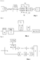
- the figure 1 is a block diagram making it possible to describe the characteristic elements of the interface according to the invention.
- the dotted blocks represent modules and optional functions of the interface according to the invention.
- the interface according to the invention will be arranged between a first device 1 generating at least two active states (two different voltages V 1 , V 2 ) and a second device 2 which will accept at least one of these two states as input.
- the voltage values corresponding to the operating states of the device are transmitted to a first optional module 10 for protection against lightning.
- the lightning protection module is, for example, a transient voltage suppression diode TVS whose limiting voltage (Reverse Stand-Off Voltage) is chosen so as not to prevent the presence of a 28V voltage continuously. on the interface input. This value will be chosen rather high to remain compatible with a given standard (for example greater than 32V). This also makes it possible to maintain a fairly low leakage current towards ground in order to limit the discharge of the battery.
- the filter stage includes several passive elements. All of the passive elements must have a low series impedance, a hundred ohms maximum, so as not to disturb the rest of the assembly.
- the filter will be made up of passive components chosen to limit the leakage current to ground as much as possible. This makes it possible to limit the discharge of the battery when the source supplying the device is a battery.
- a passive component is, for example, a resistor, an inductor, a ferrite, a capacitor.
- the device includes an optional wetting/polarization module 12.
- This optional module for wetting/biasing on on-board equipment ON voltage, referenced 12, makes it possible in particular to ensure a high wetting current as soon as the on-board voltage is present, so as not to take this wetting current on the battery voltage .
- the current value is for example between 3 and 10 mA.
- This optional block is placed between the output of the filtering stage and the divider bridges numbered 15 and 16.
- the wetting/polarization module 12 provides an optional wetting current I mopt which operates when the equipment is powered.
- the middle bias voltage module 13 provides a bias current I p which operates when the equipment is powered and on battery.
- a voltage V m is chosen bringing a default state, considered “open” by the two comparison stages 100, 200, comprising a first divider bridge 15 and a first comparator 17, and a second divider bridge 16 and a second comparator 18.
- the resistor value 131 ( figure 3 ) present in the wetting module 13 is chosen so as to limit the bias current I p to 15 ⁇ A, for example. This, always with the aim of reducing consumption on the battery and premature wear.
- a comparison chain comprises, for example, a first divider bridge 15 and a second divider bridge 16 which are arranged in parallel and downstream of the CEM filtering module. These two divider bridges make it possible in particular to adapt the level of the incoming interface to that of the thresholds fixed at the level of each comparator arranged downstream. The assembly thus makes it possible to measure active levels at 28V, even on a lower battery voltage.
- the divider bridges are made up of several resistors.
- the values of the resistors are set so as to limit the leakage current and to maintain a high input impedance against the resistances of the polarization blocks.
- a Zener DZ type diode is added to reduce the voltage value before the divider bridge, as will be detailed in picture 2 .
- the 15s output of the first divider bridge 15 and the 16s output of the second divider bridge 16 are respectively connected to a 17th input of the first comparator 17 and to an 18th input of the second comparator 18.
- comparators are chosen in particular for their temperature resistance and their low consumption because they are powered by the battery voltage.
- the input impedances of the two comparators are much higher than the input impedances of the divider bridges.
- the comparison threshold value V threshold1 and V threshold2 for each of the comparators is fixed, for example according to the supplied battery voltage and jointly with the ratios fixed by the dividing bridges. For example, for a comparator powered by a battery voltage of 5V, we will take a ratio of division by 10, which will bring a comparison voltage to 2.8V for an input at 28V. A first threshold value V threshold1 will be taken to detect the state V 1 and a second threshold value V threshold2 for the detection of the second state V 2 . For example, for a voltage of 28V, we will choose a threshold allowing detection from 12V; for ground, a threshold below 4V will be chosen for example.
- the output 17s, 18s of each of the comparators 17, 18 can be connected to a filter 19, 20 respectively which combats “glitch” type fluctuations.
- This filter is made up of passive components.
- the outputs 19s, 20s of these two optional filters 19, 20 are connected to an input 21e of a logic "OR" output module 21.
- This logical "OR” module in cooperation with the middle polarization achieved using the wetting module, allows dynamic compatibility with the 28V/Open and Open/Ground standards.
- the logical “OR” module is, for example, a NAND function with open-drain transistors and a resistive-type high draw which will be chosen so as to limit the current consumed on the battery.
- the logical operation performed by the logical "OR” module makes the output active if either of the two detection branches has seen an active 28V or GROUND level on the interface input.
- the output of the logical "OR” is connected to the second device 2 which interfaces with the first device 1.
- the picture 2 illustrates an embodiment of the mooring block on board equipment ON tension. This optional block is arranged at the "output" of the filtering stage 11, before the divider bridges 15, 16.
- This wetting block 12 consists of three elements: a reference voltage V ref1 , an adjustment resistor 121 and an isolation diode 122.
- the adjustment resistor 121 makes it possible to adjust the quantity of current supplied by the voltage reference.
- the isolation diode 122 makes it possible to avoid any disturbance of the assembly when the polarization is not present (equipment on battery only). Also, it forces the direction of the current in one and only one direction.
- the reference voltage V ref1 supplies the current I p for the polarization. Its voltage level is chosen so as not to force an active level on the interface (therefore higher than the low active threshold, and lower than the high active threshold).
- the picture 3 illustrates an embodiment of the middle wetting and biasing stage 13, for equipment in an OFF state.
- This stage includes for example a bias resistor 131, a diode 132 and a reference voltage V ref2 .
- the reference voltage V ref2 comes from the permanent source, that is to say from the battery.
- the bias resistor 131 will be chosen large enough to be able to minimize the leakage current (interface in Open mode) and still allow a little wetting current (Ground interface).
- the voltage level of the voltage reference will be chosen so that none of the downstream assemblies detects an active level on the interface.
- the value of the resistor 131 is for example chosen so that it is quite lower than the impedance of the divider bridge 15 which follows, so as not to disturb the division ratio. Indeed, even in the absence of a middle polarization in “Open” mode by the voltage of the ON equipment, a polarization is maintained with the battery. The available current being low, the idea is to limit the leakage currents of the rest of the assembly so as not to discharge the battery too quickly.
- the diode 132 makes it possible to avoid any disturbance of the assembly when the polarization is not present (equipment on battery only). Also, it forces the direction of the current in one and only one direction.
- the interface according to the invention offers in particular a dynamically interoperable interface between at least two active states and an inactive state.
- the interface advantageously makes it possible to manage the standard V+/Open interface and the Ground/Open interface. It also offers a compatible consumption of a battery or a battery thanks to a low consumption of operation.
Landscapes
- Physics & Mathematics (AREA)
- Engineering & Computer Science (AREA)
- Computer Hardware Design (AREA)
- Computing Systems (AREA)
- General Engineering & Computer Science (AREA)
- Mathematical Physics (AREA)
- Nonlinear Science (AREA)
- Amplifiers (AREA)
- Direct Current Feeding And Distribution (AREA)
- Emergency Protection Circuit Devices (AREA)
Applications Claiming Priority (1)
| Application Number | Priority Date | Filing Date | Title |
|---|---|---|---|
| FR2014249A FR3118490B1 (fr) | 2020-12-30 | 2020-12-30 | Interface discrète configurée pour gérer au moins deux états actifs et un état inactif dans un équipement |
Publications (1)
| Publication Number | Publication Date |
|---|---|
| EP4024708A1 true EP4024708A1 (de) | 2022-07-06 |
Family
ID=76375107
Family Applications (1)
| Application Number | Title | Priority Date | Filing Date |
|---|---|---|---|
| EP21217943.6A Pending EP4024708A1 (de) | 2020-12-30 | 2021-12-28 | Diskrete schnittstelle, die so konfiguriert ist, dass sie mindestens zwei aktive und einen inaktiven zustand in einem gerät verwaltet |
Country Status (2)
| Country | Link |
|---|---|
| EP (1) | EP4024708A1 (de) |
| FR (1) | FR3118490B1 (de) |
Citations (3)
| Publication number | Priority date | Publication date | Assignee | Title |
|---|---|---|---|---|
| US10365304B2 (en) | 2017-10-06 | 2019-07-30 | Ge Aviation Systems Llc | Discrete input determining circuit and method |
| CN111049119A (zh) * | 2019-12-06 | 2020-04-21 | 中国航空工业集团公司洛阳电光设备研究所 | 一种高等级雷电防护电路及设计方法 |
| US10854405B2 (en) * | 2017-02-23 | 2020-12-01 | Contemporary Amperex Technology Co., Limited | Relay diagnostic circuit |
-
2020
- 2020-12-30 FR FR2014249A patent/FR3118490B1/fr active Active
-
2021
- 2021-12-28 EP EP21217943.6A patent/EP4024708A1/de active Pending
Patent Citations (3)
| Publication number | Priority date | Publication date | Assignee | Title |
|---|---|---|---|---|
| US10854405B2 (en) * | 2017-02-23 | 2020-12-01 | Contemporary Amperex Technology Co., Limited | Relay diagnostic circuit |
| US10365304B2 (en) | 2017-10-06 | 2019-07-30 | Ge Aviation Systems Llc | Discrete input determining circuit and method |
| CN111049119A (zh) * | 2019-12-06 | 2020-04-21 | 中国航空工业集团公司洛阳电光设备研究所 | 一种高等级雷电防护电路及设计方法 |
Non-Patent Citations (1)
| Title |
|---|
| M.W. JOHNSON: "Discrete interface devices", DIGITAL AVIONICS SYSTEMS CONFERENCE, 1994. 13TH DASC., AIAA/IEEE PHOENIX, AZ, USA 30 OCT.-3 NOV. 1994, 3 November 1994 (1994-11-03), pages 309 - 317, XP055558742, ISBN: 978-0-7803-2425-1, DOI: 10.1109/DASC.1994.369464 * |
Also Published As
| Publication number | Publication date |
|---|---|
| FR3118490B1 (fr) | 2023-01-13 |
| FR3118490A1 (fr) | 2022-07-01 |
Similar Documents
| Publication | Publication Date | Title |
|---|---|---|
| EP1274106B1 (de) | Ausgleichsverfahren und -vorrichtung für einen Superkondensator | |
| FR3030155A1 (fr) | Multiplexeur analogique | |
| EP0110775A1 (de) | Regulierungseinrichtung mit kleiner Verlustspannung | |
| EP3082072A1 (de) | Empfangsblock eines rfid-tags | |
| EP1936541A1 (de) | Ein/aus Batterieladegerät mit Versorgungsschutzschaltung für eine monolithische integrierte Schaltung die verwendet die Energie von der Antenne | |
| FR3118490A1 (fr) | Interface discrète configurée pour gérer au moins deux états actifs et un état inactif dans un équipement | |
| EP3401647A1 (de) | Messsystem für den leistungspegel einer umweltenergiequelle | |
| EP3028356B1 (de) | System zur verwaltung einer versorgungsspannung eines stromnetzes an bord eines kraftfahrzeugs | |
| EP2722727B1 (de) | Zuführung einer Ladung mit Wechselpotenzial | |
| FR2943826A1 (fr) | Systeme de couplage tele-alimente avec une liaison filaire de communication, et appareil de commande d'au moins un interrupteur electronique comprenant un tel systeme de couplage | |
| EP3510685A1 (de) | Lokales analoges ausgleichssystem für eine gruppe von vorrichtungen zur speicherung von elektrischer energie mittels eines kapazitiven effekts, elektrische einrichtung, transportfahrzeug und wiederaufladbares speichermodul mit solch einem system | |
| EP4562760A1 (de) | Vorrichtung zur steuerung, zum schutz und zur überwachung des gesundheitszustands eines leistungstransistors | |
| EP3526619B1 (de) | Vorrichtung zur schnittstellenbildung zwischen einem batterieverwaltungssystem und gruppen von zellen | |
| EP3451181B1 (de) | Schutzschaltkreis gegen hohe spannungen für einen usb-empfänger vom typ c | |
| FR3072842A1 (fr) | Circuit electronique avec dispositif de surveillance de l'alimentation | |
| EP3771055B1 (de) | Güberstrom-erkennungsvorrichtung in einem elektrischen leistungsschaltkreis umfassend einen filter zur steuerung der ladung eines kondensators | |
| EP2320567A1 (de) | Schaltung zur Verbindung von Sensoren | |
| EP1113352B1 (de) | Steuervorrichtung | |
| EP0895331A1 (de) | Schutzvorrichtung für elektrische Last und Versorgungseinrichtung mit einer solchen Vorrichtung | |
| EP4184183B1 (de) | Erkennung des offenen oder geschlossenen zustandes eines leistungsschalters | |
| FR2819656A1 (fr) | Limiteur de tension pour circuit interface d'un bus de communication | |
| EP2044453B1 (de) | Vorrichtung zur messung von parametern eines elektrischen netzteils | |
| FR2835328A1 (fr) | Circuit de demarrage et de protection contre les chutes de tension d'alimentation pour un circuit sans contact | |
| FR2916278A1 (fr) | Procede de gestion d'un circuit d'une electrovanne d'un systeme de freinage electronique | |
| EP2174200A1 (de) | Schnell reagierender stromversorgungsschalter und mit einem derartigen schalter ausgerüstetes stromversorgungsnetz |
Legal Events
| Date | Code | Title | Description |
|---|---|---|---|
| PUAI | Public reference made under article 153(3) epc to a published international application that has entered the european phase |
Free format text: ORIGINAL CODE: 0009012 |
|
| STAA | Information on the status of an ep patent application or granted ep patent |
Free format text: STATUS: THE APPLICATION HAS BEEN PUBLISHED |
|
| AK | Designated contracting states |
Kind code of ref document: A1 Designated state(s): AL AT BE BG CH CY CZ DE DK EE ES FI FR GB GR HR HU IE IS IT LI LT LU LV MC MK MT NL NO PL PT RO RS SE SI SK SM TR |
|
| STAA | Information on the status of an ep patent application or granted ep patent |
Free format text: STATUS: REQUEST FOR EXAMINATION WAS MADE |
|
| 17P | Request for examination filed |
Effective date: 20221219 |
|
| RBV | Designated contracting states (corrected) |
Designated state(s): AL AT BE BG CH CY CZ DE DK EE ES FI FR GB GR HR HU IE IS IT LI LT LU LV MC MK MT NL NO PL PT RO RS SE SI SK SM TR |
|
| P01 | Opt-out of the competence of the unified patent court (upc) registered |
Effective date: 20230517 |
|
| STAA | Information on the status of an ep patent application or granted ep patent |
Free format text: STATUS: EXAMINATION IS IN PROGRESS |
|
| 17Q | First examination report despatched |
Effective date: 20250804 |