EP4027403A1 - Alliage organique pour dispositif optoélectronique organique, dispositif optoélectronique organique et dispositif d'affichage - Google Patents
Alliage organique pour dispositif optoélectronique organique, dispositif optoélectronique organique et dispositif d'affichage Download PDFInfo
- Publication number
- EP4027403A1 EP4027403A1 EP22159531.7A EP22159531A EP4027403A1 EP 4027403 A1 EP4027403 A1 EP 4027403A1 EP 22159531 A EP22159531 A EP 22159531A EP 4027403 A1 EP4027403 A1 EP 4027403A1
- Authority
- EP
- European Patent Office
- Prior art keywords
- organic
- alloy
- compound
- group
- organic compound
- Prior art date
- Legal status (The legal status is an assumption and is not a legal conclusion. Google has not performed a legal analysis and makes no representation as to the accuracy of the status listed.)
- Pending
Links
Images


Classifications
-
- H—ELECTRICITY
- H10—SEMICONDUCTOR DEVICES; ELECTRIC SOLID-STATE DEVICES NOT OTHERWISE PROVIDED FOR
- H10K—ORGANIC ELECTRIC SOLID-STATE DEVICES
- H10K85/00—Organic materials used in the body or electrodes of devices covered by this subclass
- H10K85/10—Organic polymers or oligomers
-
- C—CHEMISTRY; METALLURGY
- C09—DYES; PAINTS; POLISHES; NATURAL RESINS; ADHESIVES; COMPOSITIONS NOT OTHERWISE PROVIDED FOR; APPLICATIONS OF MATERIALS NOT OTHERWISE PROVIDED FOR
- C09K—MATERIALS FOR MISCELLANEOUS APPLICATIONS, NOT PROVIDED FOR ELSEWHERE
- C09K11/00—Luminescent materials, e.g. electroluminescent or chemiluminescent
- C09K11/02—Use of particular materials as binders, particle coatings or suspension media therefor
-
- C—CHEMISTRY; METALLURGY
- C09—DYES; PAINTS; POLISHES; NATURAL RESINS; ADHESIVES; COMPOSITIONS NOT OTHERWISE PROVIDED FOR; APPLICATIONS OF MATERIALS NOT OTHERWISE PROVIDED FOR
- C09K—MATERIALS FOR MISCELLANEOUS APPLICATIONS, NOT PROVIDED FOR ELSEWHERE
- C09K11/00—Luminescent materials, e.g. electroluminescent or chemiluminescent
- C09K11/06—Luminescent materials, e.g. electroluminescent or chemiluminescent containing organic luminescent materials
-
- C—CHEMISTRY; METALLURGY
- C23—COATING METALLIC MATERIAL; COATING MATERIAL WITH METALLIC MATERIAL; CHEMICAL SURFACE TREATMENT; DIFFUSION TREATMENT OF METALLIC MATERIAL; COATING BY VACUUM EVAPORATION, BY SPUTTERING, BY ION IMPLANTATION OR BY CHEMICAL VAPOUR DEPOSITION, IN GENERAL; INHIBITING CORROSION OF METALLIC MATERIAL OR INCRUSTATION IN GENERAL
- C23C—COATING METALLIC MATERIAL; COATING MATERIAL WITH METALLIC MATERIAL; SURFACE TREATMENT OF METALLIC MATERIAL BY DIFFUSION INTO THE SURFACE, BY CHEMICAL CONVERSION OR SUBSTITUTION; COATING BY VACUUM EVAPORATION, BY SPUTTERING, BY ION IMPLANTATION OR BY CHEMICAL VAPOUR DEPOSITION, IN GENERAL
- C23C14/00—Coating by vacuum evaporation, by sputtering or by ion implantation of the coating forming material
- C23C14/02—Pretreatment of the material to be coated
-
- H—ELECTRICITY
- H10—SEMICONDUCTOR DEVICES; ELECTRIC SOLID-STATE DEVICES NOT OTHERWISE PROVIDED FOR
- H10K—ORGANIC ELECTRIC SOLID-STATE DEVICES
- H10K50/00—Organic light-emitting devices
- H10K50/10—OLEDs or polymer light-emitting diodes [PLED]
- H10K50/11—OLEDs or polymer light-emitting diodes [PLED] characterised by the electroluminescent [EL] layers
-
- H—ELECTRICITY
- H10—SEMICONDUCTOR DEVICES; ELECTRIC SOLID-STATE DEVICES NOT OTHERWISE PROVIDED FOR
- H10K—ORGANIC ELECTRIC SOLID-STATE DEVICES
- H10K85/00—Organic materials used in the body or electrodes of devices covered by this subclass
- H10K85/60—Organic compounds having low molecular weight
- H10K85/615—Polycyclic condensed aromatic hydrocarbons, e.g. anthracene
-
- H—ELECTRICITY
- H10—SEMICONDUCTOR DEVICES; ELECTRIC SOLID-STATE DEVICES NOT OTHERWISE PROVIDED FOR
- H10K—ORGANIC ELECTRIC SOLID-STATE DEVICES
- H10K85/00—Organic materials used in the body or electrodes of devices covered by this subclass
- H10K85/60—Organic compounds having low molecular weight
- H10K85/615—Polycyclic condensed aromatic hydrocarbons, e.g. anthracene
- H10K85/622—Polycyclic condensed aromatic hydrocarbons, e.g. anthracene containing four rings, e.g. pyrene
-
- H—ELECTRICITY
- H10—SEMICONDUCTOR DEVICES; ELECTRIC SOLID-STATE DEVICES NOT OTHERWISE PROVIDED FOR
- H10K—ORGANIC ELECTRIC SOLID-STATE DEVICES
- H10K85/00—Organic materials used in the body or electrodes of devices covered by this subclass
- H10K85/60—Organic compounds having low molecular weight
- H10K85/649—Aromatic compounds comprising a hetero atom
- H10K85/654—Aromatic compounds comprising a hetero atom comprising only nitrogen as heteroatom
-
- H—ELECTRICITY
- H10—SEMICONDUCTOR DEVICES; ELECTRIC SOLID-STATE DEVICES NOT OTHERWISE PROVIDED FOR
- H10K—ORGANIC ELECTRIC SOLID-STATE DEVICES
- H10K85/00—Organic materials used in the body or electrodes of devices covered by this subclass
- H10K85/60—Organic compounds having low molecular weight
- H10K85/649—Aromatic compounds comprising a hetero atom
- H10K85/657—Polycyclic condensed heteroaromatic hydrocarbons
- H10K85/6572—Polycyclic condensed heteroaromatic hydrocarbons comprising only nitrogen in the heteroaromatic polycondensed ring system, e.g. phenanthroline or carbazole
-
- C—CHEMISTRY; METALLURGY
- C09—DYES; PAINTS; POLISHES; NATURAL RESINS; ADHESIVES; COMPOSITIONS NOT OTHERWISE PROVIDED FOR; APPLICATIONS OF MATERIALS NOT OTHERWISE PROVIDED FOR
- C09K—MATERIALS FOR MISCELLANEOUS APPLICATIONS, NOT PROVIDED FOR ELSEWHERE
- C09K2211/00—Chemical nature of organic luminescent or tenebrescent compounds
- C09K2211/10—Non-macromolecular compounds
- C09K2211/1003—Carbocyclic compounds
- C09K2211/1007—Non-condensed systems
-
- C—CHEMISTRY; METALLURGY
- C09—DYES; PAINTS; POLISHES; NATURAL RESINS; ADHESIVES; COMPOSITIONS NOT OTHERWISE PROVIDED FOR; APPLICATIONS OF MATERIALS NOT OTHERWISE PROVIDED FOR
- C09K—MATERIALS FOR MISCELLANEOUS APPLICATIONS, NOT PROVIDED FOR ELSEWHERE
- C09K2211/00—Chemical nature of organic luminescent or tenebrescent compounds
- C09K2211/10—Non-macromolecular compounds
- C09K2211/1003—Carbocyclic compounds
- C09K2211/1011—Condensed systems
-
- C—CHEMISTRY; METALLURGY
- C09—DYES; PAINTS; POLISHES; NATURAL RESINS; ADHESIVES; COMPOSITIONS NOT OTHERWISE PROVIDED FOR; APPLICATIONS OF MATERIALS NOT OTHERWISE PROVIDED FOR
- C09K—MATERIALS FOR MISCELLANEOUS APPLICATIONS, NOT PROVIDED FOR ELSEWHERE
- C09K2211/00—Chemical nature of organic luminescent or tenebrescent compounds
- C09K2211/10—Non-macromolecular compounds
- C09K2211/1018—Heterocyclic compounds
- C09K2211/1025—Heterocyclic compounds characterised by ligands
- C09K2211/1029—Heterocyclic compounds characterised by ligands containing one nitrogen atom as the heteroatom
-
- C—CHEMISTRY; METALLURGY
- C09—DYES; PAINTS; POLISHES; NATURAL RESINS; ADHESIVES; COMPOSITIONS NOT OTHERWISE PROVIDED FOR; APPLICATIONS OF MATERIALS NOT OTHERWISE PROVIDED FOR
- C09K—MATERIALS FOR MISCELLANEOUS APPLICATIONS, NOT PROVIDED FOR ELSEWHERE
- C09K2211/00—Chemical nature of organic luminescent or tenebrescent compounds
- C09K2211/10—Non-macromolecular compounds
- C09K2211/1018—Heterocyclic compounds
- C09K2211/1025—Heterocyclic compounds characterised by ligands
- C09K2211/1044—Heterocyclic compounds characterised by ligands containing two nitrogen atoms as heteroatoms
-
- C—CHEMISTRY; METALLURGY
- C09—DYES; PAINTS; POLISHES; NATURAL RESINS; ADHESIVES; COMPOSITIONS NOT OTHERWISE PROVIDED FOR; APPLICATIONS OF MATERIALS NOT OTHERWISE PROVIDED FOR
- C09K—MATERIALS FOR MISCELLANEOUS APPLICATIONS, NOT PROVIDED FOR ELSEWHERE
- C09K2211/00—Chemical nature of organic luminescent or tenebrescent compounds
- C09K2211/10—Non-macromolecular compounds
- C09K2211/1018—Heterocyclic compounds
- C09K2211/1025—Heterocyclic compounds characterised by ligands
- C09K2211/1059—Heterocyclic compounds characterised by ligands containing three nitrogen atoms as heteroatoms
-
- C—CHEMISTRY; METALLURGY
- C09—DYES; PAINTS; POLISHES; NATURAL RESINS; ADHESIVES; COMPOSITIONS NOT OTHERWISE PROVIDED FOR; APPLICATIONS OF MATERIALS NOT OTHERWISE PROVIDED FOR
- C09K—MATERIALS FOR MISCELLANEOUS APPLICATIONS, NOT PROVIDED FOR ELSEWHERE
- C09K2211/00—Chemical nature of organic luminescent or tenebrescent compounds
- C09K2211/10—Non-macromolecular compounds
- C09K2211/1018—Heterocyclic compounds
- C09K2211/1025—Heterocyclic compounds characterised by ligands
- C09K2211/1088—Heterocyclic compounds characterised by ligands containing oxygen as the only heteroatom
-
- C—CHEMISTRY; METALLURGY
- C09—DYES; PAINTS; POLISHES; NATURAL RESINS; ADHESIVES; COMPOSITIONS NOT OTHERWISE PROVIDED FOR; APPLICATIONS OF MATERIALS NOT OTHERWISE PROVIDED FOR
- C09K—MATERIALS FOR MISCELLANEOUS APPLICATIONS, NOT PROVIDED FOR ELSEWHERE
- C09K2211/00—Chemical nature of organic luminescent or tenebrescent compounds
- C09K2211/10—Non-macromolecular compounds
- C09K2211/1018—Heterocyclic compounds
- C09K2211/1025—Heterocyclic compounds characterised by ligands
- C09K2211/1092—Heterocyclic compounds characterised by ligands containing sulfur as the only heteroatom
-
- H—ELECTRICITY
- H10—SEMICONDUCTOR DEVICES; ELECTRIC SOLID-STATE DEVICES NOT OTHERWISE PROVIDED FOR
- H10K—ORGANIC ELECTRIC SOLID-STATE DEVICES
- H10K2101/00—Properties of the organic materials covered by group H10K85/00
- H10K2101/10—Triplet emission
-
- Y—GENERAL TAGGING OF NEW TECHNOLOGICAL DEVELOPMENTS; GENERAL TAGGING OF CROSS-SECTIONAL TECHNOLOGIES SPANNING OVER SEVERAL SECTIONS OF THE IPC; TECHNICAL SUBJECTS COVERED BY FORMER USPC CROSS-REFERENCE ART COLLECTIONS [XRACs] AND DIGESTS
- Y02—TECHNOLOGIES OR APPLICATIONS FOR MITIGATION OR ADAPTATION AGAINST CLIMATE CHANGE
- Y02E—REDUCTION OF GREENHOUSE GAS [GHG] EMISSIONS, RELATED TO ENERGY GENERATION, TRANSMISSION OR DISTRIBUTION
- Y02E10/00—Energy generation through renewable energy sources
- Y02E10/50—Photovoltaic [PV] energy
- Y02E10/549—Organic PV cells
Definitions
- An organic alloy for an organic optoelectric device, an organic optoelectric device, and a display device are disclosed.
- An organic optoelectric device is a device that converts electrical energy into photoenergy, and vice versa.
- An organic optoelectric device may be classified as follows in accordance with its driving principles.
- One is a photoelectric device where excitons generated by photoenergy are separated into electrons and holes and the electrons and holes are transferred to different electrodes respectively and electrical energy is generated, and the other is a light emitting device to generate photoenergy from electrical energy by supplying a voltage or a current to electrodes.
- Examples of the organic optoelectric device include an organic photoelectric device, an organic light emitting diode, an organic solar cell, and organic photo-conductor drum, and the like.
- the organic light emitting diode (OLED) has recently drawn attention due to an increase in demand for flat panel displays.
- the organic light emitting diode converts electrical energy into light by applying current to an organic light emitting material, and has a structure in which an organic layer is interposed between an anode and a cathode.
- the organic layer may include an emission layer and optionally an auxiliary layer
- the auxiliary layer may include at least one layer selected from, for example a hole injection layer, a hole transport layer, an electron blocking layer, an electron transport layer, an electron injection layer, and a hole blocking layer in order to improve efficiency and stability of an organic light emitting diode.
- Performance of an organic light emitting diode may be affected by characteristics of the organic layer, and among them, may be mainly affected by an organic material of the organic layer.
- One embodiment provides an organic alloy applicable for an organic optoelectric device.
- Another embodiment provides organic optoelectric device including the organic alloy.
- Yet another embodiment provides a display device including the organic optoelectric device.
- an organic alloy for an organic optoelectric device that is an organic alloy of at least two kinds of organic compounds, the at least two kinds of organic compounds includes a first organic compound and a second organic compound, a difference between evaporation temperatures of the first organic compound and the second organic compound is less than or equal to about 20 °C at less than or equal to about 10 -3 torr, and a light emitting wavelength of the organic alloy is different from light emitting wavelengths of the first organic compound, the second organic compound, and a simple mixture of the first organic compound and the second organic compound.
- an organic optoelectric device including an anode and a cathode facing each other, at least one organic layer interposed between the anode and the cathode, wherein the organic layer includes the organic alloy.
- a display device including the organic optoelectric device is provided.
- the present invention may provide an organic alloy having different characteristics from those of a conventional single organic compound and a simple mixture thereof and realize an organic optoelectric device having high efficiency and long life-span by applying the organic alloy to the organic optoelectric device.
- substituted refers to one substituted with deuterium, a halogen, a hydroxy group, an amino group, a substituted or unsubstituted C1 to C30 amine group, a nitro group, a substituted or unsubstituted C1 to C40 silyl group, a C1 to C30 alkyl group, a C1 to C10 alkylsilyl group, a C3 to C30 cycloalkyl group, a C2 to C30 heterocycloalkyl group, a C6 to C30 aryl group, a C2 to C30 heterocyclic group, a C1 to C20 alkoxy group, a fluoro group, a C1 to C10 trifluoroalkyl group such as a trifluoromethyl group and the like, or a cyano group, instead of at least one hydrogen of a substituent or a compound.
- the substituted C6 to C30 aryl group may be fused with another adjacent substituted C6 to C30 aryl group to form a substituted or unsubstituted fluorene ring.
- hetero refers to one including 1 to 3 hetero atoms selected from N, O, S, P and Si, and remaining carbons in one compound or substituent.
- alkyl group may refer to an aliphatic hydrocarbon group.
- the alkyl group may refer to "a saturated alkyl” without any double bond or triple bond.
- the alkyl group may be a C1 to C30 alkyl group. More specifically, the alkyl group may be a C1 to C20 alkyl group or a C1 to C10 alkyl group.
- a C1 to C4 alkyl group includes 1 to 4 carbons in alkyl chain, and may be selected from methyl, ethyl, propyl, iso-propyl, n-butyl, iso-butyl, sec-butyl, and t-butyl.
- alkyl group may be a methyl group, an ethyl group, a propyl group, an isopropyl group, a butyl group, an isobutyl group, a t-butyl group, a pentyl group, a hexyl group, a cyclopropyl group, a cyclobutyl group, a cyclopentyl group, a cyclohexyl group, and the like.
- aryl group refers to a substituent including all element of the cycle having p-orbitals which form conjugation, and may be monocyclic or fused ring polycyclic (i.e., rings sharing adjacent pairs of carbon atoms) functional group.
- heterocyclic group may refer to cyclic group including 1 to 3 hetero atoms selected from N, O, S, P and Si, and remaining carbons in a cyclic group.
- the heterocyclic group may be a fused ring where each ring may include the 1 to 3 heteroatoms.
- the substituted or unsubstituted C6 to C30 aryl group and/or the substituted or unsubstituted C2 to C30 heterocyclic group may be a substituted or unsubstituted phenyl group, a substituted or unsubstituted naphthyl group, a substituted or unsubstituted anthracenyl group, a substituted or unsubstituted phenanthryl group, a substituted or unsubstituted naphthacenyl group, a substituted or unsubstituted pyrenyl group, a substituted or unsubstituted biphenyl group, a substituted or unsubstituted p-terphenyl group, a substituted or unsubstituted m-terphenyl group, a substituted or unsubstituted chrysenyl group, a substituted or unsubstituted triphenylenyl group, a
- hole characteristics refer to characteristics capable of donating an electron to form a hole when electric field is applied, and characteristics that hole formed in the anode is easily injected into the emission layer and transported in the emission layer due to conductive characteristics according to HOMO level.
- electron characteristics refer to characteristics capable of accepting an electron when electric field is applied, and characteristics that electron formed in the cathode is easily injected into the emission layer and transported in the emission layer due to conductive characteristics according to LUMO level.
- the organic alloy is a material obtained by pre-treating more than two single organic compounds and a chemical interaction among the single organic compounds may be provided due to the pre-treatment.
- the pre-treating may be a heat treatment such as heating and sublimation followed by cooling, but is not limited thereto.
- the first and second organic compounds may have an evaporation temperature within the same or a predetermined range.
- the evaporation temperature indicates a temperature at which the first and second organic compounds may be deposited on a substrate at a predetermined rate under high vacuum of less than or equal to about 10 -3 Torr, for example, an average temperature when the first and second organic compounds are thermally evaporated to be about 300 nm to about 800 nm thick at a rate of about 0.5 to about 2 ⁇ /sec under high vacuum of less than or equal to about 10 -3 Torr.
- the difference between evaporation temperatures of the first organic compound and the second organic compound may be less than or equal to about 20 °C at less than or equal to about 10 -3 torr.
- a difference between evaporation temperatures of the first organic compound and the second organic compound may be about 0 °C to 10 °C and specifically about 0 °C to about 5 °C.
- the organic alloy has a chemical interaction among more than two single organic compounds as described above and thus, different intrinsic characteristics from the single organic compounds and their simple mixture having no chemical interaction among single organic compounds.
- the simple mixture is obtained by physically mixing single organic compounds without any pre-treatment.
- the organic alloy of the first and second organic compounds may have different intrinsic characteristics from those of the first organic compound, the second organic compound, and a simple mixture thereof, while the single mixture of the first and second organic compounds show characteristics of the first organic compound, the second organic compound, or a combination thereof.
- the light emitting wavelength of the organic alloy may be different from light emitting wavelengths of the first organic compound, the second organic compound, and a simple mixture thereof.
- the organic alloy may release new energy and emit light by a new energy bandgap between a high HOMO energy level and a low LUMO energy level of the first and second organic compounds due to intermolecular electron transfer system of the two organic compounds.
- the energy bandgap of the organic alloy may be an energy difference between LUMO energy level of the first organic compound and HOMO energy level of the second organic compound or between LUMO energy level of the second organic compound and HOMO energy level of the first organic compound.
- the simple mixture of the first and second organic compounds may have either an energy bandgap between LUMO energy and HOMO energy of the first organic compound or a bandgap between LUMO energy and HOMO energy of the second organic compound.
- the organic alloy may have a smaller or larger bandgap than that of the first organic compound, the second organic compound, and the simple mixture thereof. Accordingly, the light emitting wavelength of the organic alloy may be different from light emitting wavelengths of the first organic compound, the second organic compound, and a simple mixture thereof.
- a maximum light emitting wavelength ( ⁇ max ) of the organic alloy may be shifted greater than or equal to about 20 nm compared with a maximum light emitting wavelength of the simple mixture of the first and second organic compounds, for example, shifted greater than or equal to about 20 nm toward a long wavelength region.
- the organic alloy may have a different color from those of the first organic compound, the second organic compound, and the simple mixture thereof.
- the organic alloy may have a color with a longer wavelength region than those of the first organic compound, the second organic compound, and the simple mixture thereof.
- the organic alloy may have a different glass transition temperature (Tg) from that of the first organic compound, the second organic compound, and the simple mixture thereof.
- the organic alloy may have a different crystallization temperature (Tc) from that of the first organic compound, the second organic compound, and the simple mixture thereof.
- the organic alloy may have a different melting point (Tm) from that of the first organic compound, the second organic compound, and the simple mixture thereof. Since the glass transition temperature (Tg), the crystallization temperature (Tc), and the melting point (Tm) show inherent thermodynamic characteristics of a molecule, the compounds having the different glass transition temperature (Tg), the different crystallization temperature (Tc) and the different melting point (Tm) may be different compounds.
- the organic alloy may have inherent thermodynamic characteristics such as the glass transition temperature (Tg), the crystallization temperature (Tc), and the melting point (Tm), which may be substantially constant within an error range.
- the error range may vary depending on a measurement condition, for example, may be within about ⁇ 5 °C and specifically, within about ⁇ 2 °C. These thermodynamic characteristics may be different from those of the simple mixture of the first and second organic compounds having no inherent thermodynamic characteristics.
- the organic alloy may be pre-treated in various methods, for example, in a method of heat-treating the first and second organic compounds at greater than or equal to an evaporation temperature and liquidating or gasifying the first and second organic compounds and then, cooling and solidifying the heat-treated compounds.
- the first and second organic compounds may be melted liquid or gasified vapor at the evaporation temperature, and the pre-treated organic alloy may be a solid like a mass or powder.
- the organic alloy obtained as a solid mass may be additionally physically ground with a blender and the like.
- the organic alloy is a resulting material obtained through the aforementioned pre-treatment and may be supplied by using one source to form a thin film. Accordingly, the deposition process may become simple without a control process required when more than two organic compounds are respectively supplied by using separate sources.
- the organic alloy is a resulting material obtained through the aforementioned pre-treatment and thus, may secure uniformity and consistency for deposition compared with the more than two single organic compounds supplied by using more than two separate sources or their simple mixture of supplied by using one single source. Accordingly, when a plurality of thin films are formed through a continuous process, the organic alloy may be used to continuously produce the thin films including components in a substantially equivalent ratio and thus, increase reproducibility and reliability of the thin films.
- the first and second organic compounds may include any material having an evaporation temperature for pre-treatment at a predetermined temperature without a particular limit, for example, a compound having electron characteristics and a compound having hole characteristics to improve mobility of electrons and holes.
- the first organic compound may be a compound having relatively strong electron characteristics
- the second organic compound may be a compound having relatively strong hole characteristics
- the organic alloy of the first organic compound having relatively strong electron characteristics and the second organic compound having relatively strong hole characteristics may have bipolar characteristics.
- the first organic compound is a compound having relatively strong electron characteristics, for example a compound represented by the following Chemical Formula 1.
- the 6-membered rings substituting the triphenylene group indicate all the 6-membered rings directly or indirectly linked to the triphenylene group and include 6-membered rings including a carbon atom, a nitrogen atom, or a combination thereof.
- the first organic compound may be represented by for example the following Chemical Formula 1-1 or 1-11, depending on the bonding position of the triphenylene group.
- the first organic compound includes the triphenylene group and at least one nitrogen-containing heterocyclic group.
- the first organic compound includes at least one nitrogen-containing ring and thereby, may have a structure of easily accepting electrons when an electric field is applied thereto and thus, decrease a driving voltage of an organic optoelectric device including the first organic compound.
- the first organic compound has a bipolar structure by including both a triphenylene structure of easily accepting holes and a nitrogen-containing ring moiety of easily accepting electrons and may appropriately balance a flow of the holes and the electrons, and accordingly, improve efficiency of an organic optoelectric device when applied thereto.
- the first organic compound represented by the above Chemical Formula 1 has at least one kink structure as a center of an arylene group and/or a heterocyclic group.
- the kink structure is a structure that a linking moiety of the arylene group and/or the heterocyclic group is not a linear structure.
- a linking moiety of the arylene group and/or the heterocyclic group is not a linear structure.
- ortho phenylene (o-phenylene) and meta phenylene (m-phenylene) have the kink structure where a linking moiety does not form a linear structure
- para phenylene p-phenylene
- the kink structure may be formed as a center of a linking group (L) and/or an arylene group/a heterocyclic group.
- a kink structure may be formed as a center of an arylene group/a heterocyclic group, and for example, the compound may be represented by the following Chemical Formula 1a or 1b.
- a kink structure is formed as a center of a linking group (L), and for example, the L is may be a substituted or unsubstituted phenylene having the kink structure, a substituted or unsubstituted biphenylene group having the kink structure, or a substituted or unsubstituted terphenylene group having the kink structure.
- the L may be selected from, for example substituted or unsubstituted groups listed in the following Group 1.
- R 15 to R 42 are independently hydrogen, deuterium, a substituted or unsubstituted C1 to C10 alkyl group, a substituted or unsubstituted C3 to C30 cycloalkyl group, a substituted or unsubstituted C2 to C30 heterocycloalkyl group, a substituted or unsubstituted C6 to C30 aryl group, a substituted or unsubstituted C2 to C30 heterocyclic group, a substituted or unsubstituted amine group, a substituted or unsubstituted C6 to C30 arylamine group, a substituted or unsubstituted C6 to C30 heteroarylamine group, a substituted or unsubstituted C1 to C30 alkoxy group, a halogen, a halogen-containing group, a cyano group, a hydroxyl group, an amino group, a nitro group, a carboxyl group,
- the first organic compound may have at least two kink structures and for example, two to four kink structures.
- the first organic compound may appropriately localize charges and control a conjugation-system flow due to the above kink structure, and thus improve a life-span of an organic optoelectric device to which the composition is applied.
- the number of R 1 to R 6 that is the total number of 6-membered rings substituting the triphenylene group is limited to be less than or equal to 6, and thereby thermal decomposition of the compound by a high temperature during a deposition process may be decreased.
- the first organic compound may be effectively prevented from stacking depending on the structure and decrease process stability and simultaneously, a deposition temperature.
- This stacking prevention effect may be further increased when the compound includes the linking group (L) of the above Chemical Formula 1.
- the first organic compound may be, for example represented by one of the following Chemical Formulae 1c to 1t.
- the first organic compound may be, for example, a compound listed in the following Group 2 but is not limited thereto.
- At least one or more kinds of the first organic compound may be used.
- the second organic compound may be a compound having relatively strong hole characteristics, for example, a compound represented by the following Chemical Formula 2.
- the second organic compound is a compound having bipolar characteristics in which hole characteristics are relatively stronger than electron characteristics and thus, increases charge mobility and stability by forming an organic alloy with the first organic compound and resultantly, may improve luminous efficiency and life-span characteristics.
- Ar 1 and Ar 2 of the above Chemical Formula 2 are substitutents having hole or electron characteristics, and may be independently for example a substituted or unsubstituted phenyl group, a substituted or unsubstituted biphenyl group, a substituted or unsubstituted terphenyl group, a substituted or unsubstituted naphthyl group, a substituted or unsubstituted anthracenyl group, , a substituted or unsubstituted triphenylenyl group, a substituted or unsubstituted carbazolyl group, a substituted or unsubstituted benzofuranyl group, a substituted or unsubstituted benzothiophenyl group, a substituted or unsubstituted fluorenyl group, a substituted or unsubstituted pyridyl group, a substituted or unsubstituted pyrimidinyl group, a substituted
- At least one of Ar 1 and Ar 2 of the above Chemical Formula 2 may be for example substituents having electron characteristics, and may be for example substituents represented by the following Chemical Formula A.
- the substituent represented by the above Chemical Formula A may be for example one of functional groups listed in the following Group 3.
- At least one of Ar 1 and Ar 2 of the above Chemical Formula 2 may be, for example a substituent having hole characteristics, and may be, for example substituents listed in the following Group 4.
- the compound represented by the above Chemical Formula 2 may be, for example selected from compounds listed in the following Group 5, but is not limited thereto.
- At least one or more kinds of the second organic compound may be used.
- first and second organic compounds may be variously combined to prepare various organic alloys.
- the first organic compound may be at least one of compounds listed in the following Group A
- the second organic compound may be at least one of compounds listed in the following Group B, but they are not limited thereto.
- the first organic compound is a compound having relatively strong electron characteristics
- the second organic compound is a compound having relatively strong hole characteristics
- they are pre-treated to form an organic alloy to increase mobility of electrons and holes and thus, to remarkably improve luminous efficiency compared with when the first compound or the second compound is used at alone.
- excitons When the single material having biased towardelectron characteristics or biased toward hole characteristics is used to form an emission layer, excitons may be relatively more formed at an interface of an emission layer and the electron transport layer (ETL) or hole transport layer (HTL). As a result, the excitons in the emission layer may interact with charges at the interface of the electron transport layer (ETL) or the hole transport layer (HTL) and thus, cause a roll-off of sharply deteriorating efficiency and also, sharply deteriorate light emitting life-span characteristics.
- ETL electron transport layer
- HTL hole transport layer
- the organic alloy of the first organic compound and the second organic compound is introduced into the emission layer to manufacture a device balancing carriers in the emission layer, so that a light emitting area may not be biased toward either the electron transport layer (ETL) or hole transport layer (HTL) and thus, remarkably improving roll-off and simultaneously life-span characteristics.
- ETL electron transport layer
- HTL hole transport layer
- the organic alloy may be obtained by using the first organic compound and the second organic compound in a mole ratio, for example about 1:10 to about 10:1. As another examples, the organic alloy may be obtained by using the first organic compound and the second organic compound in a mole ratio of about 1:4 to about 4:1, or in a mole ratio of about 1: 1.
- bipolar characteristics may be realized more efficiently and efficiency and life-span may be improved.
- the organic alloy may be obtained by pre-treating the above first organic compound and second organic compound, or may be obtained by pre-treating at least one kind of an organic compound besides the above first organic compound and second organic compound.
- the organic alloy may be used as an organic material for an organic optoelectric device, and may be used as, for example a light emitting material, a light absorbing material, a charge transport material, a charge injection material, a charge blocking material, or a combination thereof.
- the organic alloy may be used as a light emitting material for an organic optoelectric device.
- the organic alloy may be used as a host, and may further include at least one kind of a dopant.
- the dopant may be a red, green, or blue dopant, for example a phosphorescent dopant.
- the dopant is mixed with the organic alloy in a small amount to cause light emission, and may be generally a material such as a metal complex that emits light by multiple excitation into a triplet or more.
- the dopant may be, for example an inorganic, organic, or organic/inorganic compound, and one or more kinds thereof may be used.
- Examples of the phosphorescent dopant may be an organic metal compound including Ir, Pt, Os, Ti, Zr, Hf, Eu, Tb, Tm, Fe, Co, Ni, Ru, Rh, Pd, or a combination thereof.
- the phosphorescent dopant may be, for example a compound represented by the following Chemical Formula Z, but is not limited thereto. [Chemical Formula Z] L 2 MX
- M is a metal
- L and X are the same or different, and are a ligand to form a complex compound with M.
- the M may be, for example Ir, Pt, Os, Ti, Zr, Hf, Eu, Tb, Tm, Fe, Co, Ni, Ru, Rh, Pd, or a combination thereof, and the L and X may be, for example a bidendate ligand.
- the organic material may form a film using a dry film-forming method such as chemical vapor deposition or a solution process.
- the organic optoelectric device may be any device to convert electrical energy into photoenergy and vice versa without particular limitation, and may be, for example an organic photoelectric device, an organic light emitting diode, an organic solar cell, and an organic photo-conductor drum.
- the organic optoelectric device includes an anode and a cathode facing each other, and at least one organic layer interposed between the anode and the cathode, wherein the organic layer includes the above organic material.
- FIGS. 1 and 2 are cross-sectional views of each organic light emitting diode according to one embodiment.
- an organic light emitting diode 100 includes an anode 120 and a cathode 110 facing each other and an organic layer 105 interposed between the anode 120 and cathode 110.
- the anode 120 may be made of a conductor having a large work function to help hole injection, and may be for example metal, metal oxide and/or a conductive polymer.
- the anode 120 may be a metal such as nickel, platinum, vanadium, chromium, copper, zinc, gold, and the like or an alloy thereof; metal oxide such as zinc oxide, indium oxide, indium tin oxide (ITO), indium zinc oxide (IZO), and the like; a combination of metal and oxide such as ZnO and Al or SnO 2 and Sb; a conductive polymer such as poly(3-methylthiophene), poly(3,4-(ethylene-1,2-dioxy)thiophene) (PEDOT), polypyrrole, and polyaniline, but is not limited thereto.
- the cathode 110 may be made of a conductor having a small work function to help electron injection, and may be for example metal, metal oxide and/or a conductive polymer.
- the cathode 110 may be for example a metal or an alloy thereof such as magnesium, calcium, sodium, potassium, titanium, indium, yttrium, lithium, gadolinium, aluminum silver, tin, lead, cesium, barium, and the like; a multi-layer structure material such as LiF/AI, LiO 2 /Al, LiF/Ca, LiF/AI and BaF 2 /Ca, but is not limited thereto.
- the organic layer 105 may include an emission layer 130 including the above organic material.
- the emission layer 130 may include, for example the above organic material.
- an organic light emitting diode 200 further includes a hole auxiliary layer 140 as well as an emission layer 130.
- the hole auxiliary layer 140 may further increase hole injection and/or hole mobility between the anode 120 and emission layer 130 and block electrons.
- the hole auxiliary layer 140 may be, for example a hole transport layer (HTL), a hole injection layer (HIL), and/or an electron blocking layer (EBL), and may include at least one layer.
- HTL hole transport layer
- HIL hole injection layer
- EBL electron blocking layer
- an organic light emitting diode may further include an electron transport layer (ETL), an electron injection layer (EIL), a hole injection layer (HIL), and the like, in an organic layer 105 in FIG. 1 or FIG. 2 .
- ETL electron transport layer
- EIL electron injection layer
- HIL hole injection layer
- the organic light emitting diodes 100 and 200 may be manufactured by forming an anode or a cathode on a substrate, forming an organic layer in accordance with a dry coating method such as evaporation, sputtering, plasma plating, and ion plating; and forming a cathode or an anode thereon.
- a dry coating method such as evaporation, sputtering, plasma plating, and ion plating
- the organic light emitting diode may be applied to an organic light emitting diode (OLED) display.
- OLED organic light emitting diode
- the compound A-33 had an evaporation temperature of about 226 ⁇ 10°C under less than or equal to 10 -3 Torr.
- the compound B-10 had an evaporation temperature of about 225 ⁇ 10° C under less than or equal to 10 -3 Torr.
- the compound B-43 had an evaporation temperature of about 232 ⁇ 10 °C under less than or equal to 10 -3 Torr.
- a powder-type organic alloy was obtained by putting the compound A-33 and the compound B-10 in a mole ratio of 1:1 in a vacuum chamber of less than or equal to 10 -3 Torr, melting the compound A-33 and the compound B-10 by increasing temperature of the vacuum chamber, solidifying them by cooling down to room temperature of 25 °C, and grinding the solid with a blender.
- a powder-type organic alloy was obtained by putting the compound A-33 and the compound B-43 in a mole ratio of 1:1 in a vacuum chamber of less than or equal to 10 -3 Torr, melting the compound A-33 and the compound B-43 by increasing temperature of the vacuum chamber, solidifying them by cooling down to room temperature of 25 °C, and grinding the solid with a blender.
- a powder-type compound A-33 was prepared by grinding the compound A-33 according to Synthesis Example 5 with a blender at room temperature (25 °C).
- the powder-type compound B-10 was prepared by grinding the compound B-10 according to Synthesis Example 1 of a second organic compound at temperature (25 °C) with a blender.
- a powder-type compound B-43 was obtained by grinding the compound B-43 according to Synthesis Example 2 of a second organic compound at room temperature (25 °C) with a blender.
- the compound A-33 according to Synthesis Example 5 and the compound B-43 according to Synthesis Example 1 of a second organic compound were physically ground in a mole ratio of 1:1 at room temperature (25 °C) with a blender, preparing a simple mixture.
- Optical properties of the organic alloys according to Examples 1 and 2 and the organic materials according to Comparative Examples 1 to 5 were evaluated.
- the optical properties were evaluated by measuring photoluminescence (PL) spectrum of powders of the organic alloys according to Examples 1 and 2 and the organic materials according to Comparative Examples 1 to 5 with a Fluorescence spectrophotometer (F-4500, Hitachi).
- the powders were used as a sample, and herein, a solid sample holder of 650-0161 (Hitachi) was used as a PL holder.
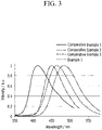
- FIG. 3 is a graph showing light emitting characteristics of the organic alloy according to Example 1 and the organic materials according to Comparative Examples 1 to 3 depending on a wavelength
- FIG. 4 is a graph showing light emitting characteristics of the organic alloy according to Example 2 and the organic materials according to Comparative Examples 1, 4, and 5 depending on a wavelength.
- Table 1 Maximum light emitting wavelength ⁇ max (nm) eV Example 1 483 2.57 Comparative Example 1 411 3.02 Comparative Example 2 449 2.76 Comparative Example 3 463 2.78
- Table 2 Maximum light emitting wavelength ⁇ max (nm) eV Example 2 488 2.55 Comparative Example 1 411 3.02 Comparative Example 4 420 2.95 Comparative Example 5 421 2.95
- the organic alloy of Example 1 showed different optical properties from the organic materials according to Comparative Examples 1 to 3
- the organic alloy of Example 2 showed different optical properties from the organic materials according to Comparative Examples 1, 4, and 5.
- the organic alloy of Example 1 showed inherent optical properties differing from those of the first organic compound A-33 and the second organic compound B-10, for example, a maximum light emitting wavelength greater than or equal to about 20nm moving toward a long wavelength, while the organic material of Comparative Example 3, that is, a simple mixture of the first organic compound A-33 and the second organic compound B-10, showed optical properties of the first organic compound A-33, the second organic compound B-10, or a combination thereof.
- the organic alloy of Example 2 showed inherent optical properties differing from those of the first organic compound A-33 and the second organic compound B-43, for example, a maximum light emitting wavelength greater than or equal to about 20 nm toward a long wavelength, while the organic material of Comparative Example 5, that is, a simple mixture of the first organic compound A-33 and the second organic compound B-43 showed optical properties of the first organic compound A-33, the second organic compound B-43, or a combination thereof.
- the organic alloy according to Example 1 showed inherent energy level differing from those of the first organic compound A-33 and the second organic compound B-10, while the organic material of Comparative Example 3, that is, a mixture of the first organic compound A-33 and the second organic compound B-10, showed substantially similar energy level to that of the first organic compound A-33 or the second organic compound B-10.
- the organic alloy of Example 2 showed inherent energy level differing from those of first organic compound A-33 and the second organic compound B-43, while the organic material of Comparative Example 5, that is, a simple mixture of the first organic compound A-33 and the second organic compound B-43 showed substantially similar energy level to that of the first organic compound A-33 or the second organic compound B-43.
- thermodynamic characteristics of the organic alloys of Examples 1 and 2 and the organic materials of Comparative Examples 1 to 5 were evaluated.
- the thermodynamic characteristics of the organic alloys of Examples 1 and 2 and the organic materials of Comparative Examples 1 to 5 were measured through differential scanning calorimetry by using DSC1 (Mettler-Toledo Inc.).
- the organic alloy of Example 1 showed different thermodynamic characteristics from those of the organic materials of Comparative Examples 1 to 3, and the organic alloy of Example 2 showed different thermodynamic characteristics from the organic materials according to Comparative Examples 1, 4, and 5.
- the organic alloy of Example 1 showed inherent thermodynamic characteristics differing from those of the first organic compound A-33, the second organic compound B-10, and a simple mixture thereof, while the organic material of Comparative Example 3, that is, a simple mixture of the first organic compound A-33 and the second organic compound B-10 showed substantially similar thermodynamic characteristics to those of the organic material of Comparative Example 2.
- the organic alloy of Example 2 showed different thermodynamic characteristics from those of the first organic compound A-33, the second organic compound B-43, and a simple mixture of the first organic compound A-33 and the second organic compound B-43, while the organic material of Comparative Example 5, a simple mixture of the first organic compound A-33 and the second organic compound B-43 showed substantially similar thermodynamic characteristics to those of the organic material of Comparative Example 4, that is, the second organic compound B-43.
- thermodynamic characteristics of the organic alloy of Examples 1 and 2 and organic materials of Comparative Examples 3 and 5 was evaluated. The consistency of thermodynamic characteristics was evaluated by more than once measuring the thermodynamic characteristics of Evaluation 2 and seeing if the measurements were constant.
- the organic alloys of Examples 1 and 2 showed constant melting points within an error range of ⁇ 5 °C, especially, within an error range of ⁇ 2 °C over more than one measurement, while the organic materials of Comparative Examples 3 and 5 showed largely different melting points over the measurements, for example, within an error range of about 20 °C. Accordingly, the organic alloys of Examples 1 and 2 showed more constant organic thermodynamic characteristics than a single organic compound or a simple mixture thereof.
- the variation with time during continuous process was evaluated by continuously depositing the organic alloys of Examples 1 and 2 and the organic materials of Comparative Examples 3 and 5 on a glass substrate to form a plurality of films and examining if single organic compounds constantly maintained a ratio in each film through a high performance liquid chromatography (HPLC) analysis method.
- HPLC high performance liquid chromatography
- the films formed of the organic alloys according to Examples 1 and 2 showed almost constant ratio among single organic compounds, that is, A-33/B-10 or A-33/B-43 compared with the thin films formed of the organic materials according to Comparative Examples 3 and 5. Accordingly, a thin film formed of an organic alloy may be reproduced through a continuous process compared with a thin film formed of a simple mixture.
- a glass substrate coated with a 1500 ⁇ -thick ITO (Indium tin oxide) was cleaned with distilled water and an ultrasonic wave.
- glass substrate was ultrasonic wave-cleaned with a solvent such as isopropyl alcohol, acetone, methanol and the like and dried, and then, moved to a plasma cleaner, cleaned by using oxygen plasma for 10 minutes and to a vacuum depositor.
- a solvent such as isopropyl alcohol, acetone, methanol and the like
- HIL hole injection layer
- HTL hole transport layer
- a 400 ⁇ -thick emission layer was formed by vacuum-depositing the organic alloy of Example 1 as a host doped with 10 wt% of tris(4-methyl-2,5-diphenylpyridine)iridium (III) (the compound D) as a dopant.
- a 300 ⁇ -thick electron transport layer (ETL) was formed on the emission layer by vacuum-depositing 8-(4-(4-(naphthalen-2-yl)-6-(naphthalen-3-yl)-1,3,5-triazin-2-yl)phenyl)quinoline (the compound E) and simultaneously hydroxyquinoline lithium (Liq) in a ratio of 1:1, and a cathode was formed on the electron transport layer (ETL) by sequentially vacuum-depositing Liq to be 15 ⁇ thick and Al to be 1200 ⁇ thick, manufacturing an organic light emitting diode.
- ETL electron transport layer
- the organic light emitting diode had a structure of five-story organic thin films and specifically,
- An organic light emitting diode was manufactured according to the same method as Example 3 except for using the organic alloy of Example 2 instead of the organic alloy of Example 1.
- An organic light emitting diode was manufactured according to the same method as Example 3 except for using the organic material of Comparative Example 1, that is, the compound A-33 as a single host instead of the organic alloy of Example 1.
- An organic light emitting diode was manufactured according to the same method as Example 3 except for using the organic material of Comparative Example 2, that is, the compound B-10 as a single host instead of the organic alloy of Example 1.
- An organic light emitting diode was manufactured according to the same method as Example 3 except for using the organic material of Comparative Example 3, that is, a simple mixture of the compound A-33 and the compound B-10 instead of the organic alloy of Example 1.
- An organic light emitting diode was manufactured according to the same method as Example 3 except for using the organic material of Comparative Example 4, that is, the compound B-43 as a single host instead of the organic alloy of Example 1.
- An organic light emitting diode was manufactured according to the same method as Example 3 except for using the organic material of Comparative Example 5, that is, a simple mixture of the compound A-33 and the compound B-43instead of the organic alloy of Example 1.
- Luminance of the manufactured organic light emitting diodes was measured for luminance, while increasing the voltage from 0 V to 10 V using a luminance meter (Minolta Cs-1000A).
- Luminance (cd/m 2 ) was maintained at 6000 cd/m 2 and a time at current efficiency (cd/A) decreases to 97 % was measured.
- Table 9 Host Luminous efficiency (cd/A) Life-spanT97 (h)
- Example3 A-33+B-10 organic alloy 47.7 450 Comparative Example6 A-33 31.1 150 Comparative Example7 B-10 34.8 10 Comparative Example8 A-33+B-10 simple mixture 45.1 350 (Table 10)
- Example4 A-33+B-43 organic alloy 47.8 900 Comparative Example6 A-33 31.1 150 Comparative Example9 B-43 2.6 10 Comparative Example10 A-33+B-43 simple mixture 44.0 720
- the organic light emitting diode of Example 3 showed equivalent or improved luminous efficiency and life-span characteristics compared with the organic light emitting diodes of Comparative Examples 6 to 8, and the organic light emitting diode of Example 4 showed equivalent or improved luminous efficiency and life-span characteristics compared with the organic light emitting diodes of Comparative Examples 6, 9, and 10. Accordingly, an organic light emitting diode using the organic alloy turned out to have equivalent or improved performance compared with an organic light emitting diode using a single organic compound or a simple mixture thereof.
Landscapes
- Chemical & Material Sciences (AREA)
- Engineering & Computer Science (AREA)
- Materials Engineering (AREA)
- Physics & Mathematics (AREA)
- Spectroscopy & Molecular Physics (AREA)
- Organic Chemistry (AREA)
- Metallurgy (AREA)
- Mechanical Engineering (AREA)
- Chemical Kinetics & Catalysis (AREA)
- Optics & Photonics (AREA)
- Electroluminescent Light Sources (AREA)
- Plural Heterocyclic Compounds (AREA)
- Indole Compounds (AREA)
- Physical Vapour Deposition (AREA)
Applications Claiming Priority (3)
| Application Number | Priority Date | Filing Date | Title |
|---|---|---|---|
| KR1020130121569A KR101812581B1 (ko) | 2013-10-11 | 2013-10-11 | 유기광전자소자용 유기합화물, 유기 광전자 소자 및 표시 장치 |
| EP14852613.0A EP3056554B1 (fr) | 2013-10-11 | 2014-06-17 | Alliage organique pour dispositif optoélectronique organique, dispositif optoélectronique organique et dispositif d'affichage |
| PCT/KR2014/005306 WO2015053459A1 (fr) | 2013-10-11 | 2014-06-17 | Alliage organique pour dispositif optoélectronique organique, dispositif optoélectronique organique et dispositif d'affichage |
Related Parent Applications (2)
| Application Number | Title | Priority Date | Filing Date |
|---|---|---|---|
| EP14852613.0A Division EP3056554B1 (fr) | 2013-10-11 | 2014-06-17 | Alliage organique pour dispositif optoélectronique organique, dispositif optoélectronique organique et dispositif d'affichage |
| EP14852613.0A Division-Into EP3056554B1 (fr) | 2013-10-11 | 2014-06-17 | Alliage organique pour dispositif optoélectronique organique, dispositif optoélectronique organique et dispositif d'affichage |
Publications (1)
| Publication Number | Publication Date |
|---|---|
| EP4027403A1 true EP4027403A1 (fr) | 2022-07-13 |
Family
ID=52813259
Family Applications (3)
| Application Number | Title | Priority Date | Filing Date |
|---|---|---|---|
| EP22159528.3A Pending EP4027402A1 (fr) | 2013-10-11 | 2014-06-17 | Alliage organique pour dispositif optoélectronique organique, dispositif optoélectronique organique et dispositif d'affichage |
| EP22159531.7A Pending EP4027403A1 (fr) | 2013-10-11 | 2014-06-17 | Alliage organique pour dispositif optoélectronique organique, dispositif optoélectronique organique et dispositif d'affichage |
| EP14852613.0A Active EP3056554B1 (fr) | 2013-10-11 | 2014-06-17 | Alliage organique pour dispositif optoélectronique organique, dispositif optoélectronique organique et dispositif d'affichage |
Family Applications Before (1)
| Application Number | Title | Priority Date | Filing Date |
|---|---|---|---|
| EP22159528.3A Pending EP4027402A1 (fr) | 2013-10-11 | 2014-06-17 | Alliage organique pour dispositif optoélectronique organique, dispositif optoélectronique organique et dispositif d'affichage |
Family Applications After (1)
| Application Number | Title | Priority Date | Filing Date |
|---|---|---|---|
| EP14852613.0A Active EP3056554B1 (fr) | 2013-10-11 | 2014-06-17 | Alliage organique pour dispositif optoélectronique organique, dispositif optoélectronique organique et dispositif d'affichage |
Country Status (7)
| Country | Link |
|---|---|
| US (3) | US20160141505A1 (fr) |
| EP (3) | EP4027402A1 (fr) |
| JP (4) | JP6769873B2 (fr) |
| KR (1) | KR101812581B1 (fr) |
| CN (2) | CN112563430A (fr) |
| TW (1) | TWI549331B (fr) |
| WO (1) | WO2015053459A1 (fr) |
Families Citing this family (37)
| Publication number | Priority date | Publication date | Assignee | Title |
|---|---|---|---|---|
| CN102473857A (zh) | 2010-01-15 | 2012-05-23 | 出光兴产株式会社 | 有机电致发光元件 |
| KR101812581B1 (ko) | 2013-10-11 | 2017-12-27 | 제일모직 주식회사 | 유기광전자소자용 유기합화물, 유기 광전자 소자 및 표시 장치 |
| US10297762B2 (en) | 2014-07-09 | 2019-05-21 | Universal Display Corporation | Organic electroluminescent materials and devices |
| US10749113B2 (en) | 2014-09-29 | 2020-08-18 | Universal Display Corporation | Organic electroluminescent materials and devices |
| US10361375B2 (en) | 2014-10-06 | 2019-07-23 | Universal Display Corporation | Organic electroluminescent materials and devices |
| KR101829749B1 (ko) | 2014-10-31 | 2018-02-19 | 삼성에스디아이 주식회사 | 유기 광전자 소자용 화합물, 유기 광전자 소자용 조성물, 유기 광전자 소자 및 표시 장치 |
| KR101888934B1 (ko) | 2015-04-24 | 2018-08-16 | 삼성에스디아이 주식회사 | 유기 광전자 소자용 화합물, 유기 광전자 소자 및 표시장치 |
| CN106316925A (zh) * | 2015-06-26 | 2017-01-11 | 上海和辉光电有限公司 | 一种有机电致发光化合物及其应用 |
| US11522140B2 (en) | 2015-08-17 | 2022-12-06 | Universal Display Corporation | Organic electroluminescent materials and devices |
| CN109790120A (zh) * | 2016-11-23 | 2019-05-21 | 广州华睿光电材料有限公司 | 含氮杂咔唑衍生物的有机混合物及其应用 |
| US20190319197A1 (en) * | 2016-11-23 | 2019-10-17 | Guangzhou Chinaray Optoelectronic Materials Ltd. | Organic compound, applications thereof, organic mixture, and organic electronic device |
| KR20180081646A (ko) * | 2017-01-06 | 2018-07-17 | 삼성디스플레이 주식회사 | 유기 발광 소자 |
| KR102275343B1 (ko) | 2017-02-28 | 2021-07-09 | 삼성에스디아이 주식회사 | 유기 광전자 소자용 조성물, 유기 광전자 소자 및 표시 장치 |
| KR20180137772A (ko) * | 2017-06-19 | 2018-12-28 | 삼성에스디아이 주식회사 | 유기 광전자 소자 및 표시 장치 |
| CN109206408A (zh) * | 2017-06-29 | 2019-01-15 | 祥德科技股份有限公司 | 可作为发光材料的双极化合物及使用该双极化合物的有机发光元件 |
| KR101856728B1 (ko) | 2017-08-10 | 2018-05-10 | 주식회사 엘지화학 | 유기 발광 소자 |
| KR20190070586A (ko) | 2017-12-13 | 2019-06-21 | 엘지디스플레이 주식회사 | 전자수송 재료용 화합물 및 이를 포함하는 유기 발광 다이오드 |
| KR102235989B1 (ko) * | 2018-06-14 | 2021-04-05 | 주식회사 엘지화학 | 화합물 및 이를 포함하는 유기 발광 소자 |
| TWI660028B (zh) * | 2018-07-13 | 2019-05-21 | 祥德科技股份有限公司 | 用於有機發光元件的發光層主體材料 |
| US12193324B2 (en) | 2019-03-25 | 2025-01-07 | Nippon Steel Chemical & Material Co., Ltd. | Melt mixture for organic electroluminescent element, and organic electroluminescent element |
| KR102275039B1 (ko) * | 2019-10-08 | 2021-07-08 | 엘티소재주식회사 | 유기 발광 소자, 이의 제조 방법 및 유기 발광 소자의 유기물층용 조성물 |
| KR20220061004A (ko) | 2020-11-05 | 2022-05-12 | 롬엔드하스전자재료코리아유한회사 | 복수 종의 호스트 재료, 이를 포함하는 조성물, 및 이를 포함하는 유기 전계 발광 소자 |
| WO2022231390A1 (fr) * | 2021-04-30 | 2022-11-03 | 주식회사 엘지화학 | Dispositif électroluminescent organique |
| JP7707508B2 (ja) * | 2021-04-30 | 2025-07-15 | エルジー・ケム・リミテッド | 有機発光素子 |
| EP4270509A4 (fr) * | 2021-04-30 | 2024-08-07 | Lg Chem, Ltd. | Dispositif électroluminescent organique |
| CN116803234A (zh) * | 2021-04-30 | 2023-09-22 | 株式会社Lg化学 | 有机发光器件 |
| KR102803915B1 (ko) * | 2021-05-06 | 2025-05-08 | 주식회사 엘지화학 | 유기 발광 소자 |
| WO2022235101A1 (fr) * | 2021-05-06 | 2022-11-10 | 주식회사 엘지화학 | Dispositif électroluminescent organique |
| KR20220151981A (ko) * | 2021-05-07 | 2022-11-15 | 주식회사 엘지화학 | 유기 발광 소자 |
| KR102753279B1 (ko) * | 2021-05-07 | 2025-01-14 | 주식회사 엘지화학 | 유기 발광 소자 |
| JP7646987B2 (ja) * | 2021-05-07 | 2025-03-18 | エルジー・ケム・リミテッド | 有機発光素子 |
| US20240407244A1 (en) * | 2021-10-14 | 2024-12-05 | Idemitsu Kosan Co.,Ltd. | Mixed powder for an organic electroluminescence device and method for producing the same, method for fabricating organic electroluminescence device by using the mixed powder, method for selecting compounds in the mixed powder, and composition for vacuum deposition |
| WO2023100891A1 (fr) * | 2021-11-30 | 2023-06-08 | 出光興産株式会社 | Mélange fondu solide, composition solide, poudre mélangée, procédé de sélection de composé organique, procédé de production de mélange fondu solide et procédé de production d'élément électroluminescent organique |
| WO2023171544A1 (fr) * | 2022-03-08 | 2023-09-14 | 出光興産株式会社 | Poudre mélangée, procédé de fabrication de poudre mélangée, composition, élément électroluminescent organique et procédé de fabrication d'élément électroluminescent organique |
| KR102577795B1 (ko) * | 2022-06-10 | 2023-09-12 | 솔루스첨단소재 주식회사 | 유기 전계 발광 소자용 균일상 유기 복합체 및 이를 포함하는 유기 전계 발광 소자 |
| KR102487491B1 (ko) * | 2022-06-13 | 2023-01-12 | 솔루스첨단소재 주식회사 | 유기 전계 발광 소자용 펠릿 및 이를 이용한 유기 전계 발광 소자 |
| KR102661530B1 (ko) * | 2023-10-20 | 2024-04-26 | 솔루스첨단소재 주식회사 | 균일상 유기 복합체의 제조방법 및 이로부터 제조된 균일상 유기 복합체, 상기 균일상 유기 복합체를 포함하는 유기 전계 발광 소자 |
Citations (4)
| Publication number | Priority date | Publication date | Assignee | Title |
|---|---|---|---|---|
| EP1156536A2 (fr) | 2000-05-19 | 2001-11-21 | Eastman Kodak Company | Procédé d'utilisation de materiaux dopés en avance dans la fabricage d'un dispositif organique émetteur de lumière |
| US20060134464A1 (en) * | 2004-12-22 | 2006-06-22 | Fuji Photo Film Co. Ltd | Organic electroluminescent element |
| JP2006203172A (ja) * | 2004-12-22 | 2006-08-03 | Fuji Photo Film Co Ltd | 有機電界発光素子 |
| WO2011136755A1 (fr) * | 2010-04-28 | 2011-11-03 | Universal Display Corporation | Dépôt de matériaux pré-mélangés |
Family Cites Families (43)
| Publication number | Priority date | Publication date | Assignee | Title |
|---|---|---|---|---|
| JP3139321B2 (ja) | 1994-03-31 | 2001-02-26 | 東レ株式会社 | 発光素子 |
| US5853905A (en) | 1997-09-08 | 1998-12-29 | Motorola, Inc. | Efficient single layer electroluminescent device |
| JP2000223268A (ja) * | 1999-01-27 | 2000-08-11 | Toray Ind Inc | 有機電界発光素子の製造方法 |
| JP2002146516A (ja) | 2000-11-07 | 2002-05-22 | Sony Corp | 有機薄膜の蒸着方法 |
| JP2003045650A (ja) | 2001-07-17 | 2003-02-14 | Kiko Kenji Kagi Kofun Yugenkoshi | 有機el素子の製造装置 |
| JP2003347059A (ja) * | 2002-05-27 | 2003-12-05 | Tdk Corp | 有機el素子 |
| JP3745724B2 (ja) | 2002-10-31 | 2006-02-15 | 富士電機ホールディングス株式会社 | 昇華性材料の蒸着用ルツボおよび該ルツボを使用した蒸着方法 |
| US20050056960A1 (en) * | 2003-09-16 | 2005-03-17 | Eastman Kodak Company | Forming homogeneous mixtures of organic materials for physical vapor deposition using melting |
| JP4622433B2 (ja) | 2003-10-06 | 2011-02-02 | 三菱化学株式会社 | 化合物、電子輸送材料および有機電界発光素子 |
| KR100721565B1 (ko) | 2004-11-17 | 2007-05-23 | 삼성에스디아이 주식회사 | 저분자 유기 전계 발광 소자 및 그의 제조 방법 |
| JP4882444B2 (ja) | 2006-03-27 | 2012-02-22 | 株式会社デンソー | 有機el素子 |
| JP2007270280A (ja) | 2006-03-31 | 2007-10-18 | Kyocera Corp | 蒸着装置、有機el装置の製造方法、蒸着方法、及び蒸着用セル |
| KR100762014B1 (ko) * | 2006-07-24 | 2007-10-04 | 제일모직주식회사 | 유기이온염을 포함하는 전도성 고분자 조성물 및 이를이용한 유기 광전 소자 |
| JP2009027091A (ja) * | 2007-07-23 | 2009-02-05 | Sony Corp | 有機電界発光素子および表示装置 |
| KR102189768B1 (ko) | 2007-08-08 | 2020-12-14 | 유니버셜 디스플레이 코포레이션 | 인광성 발광 다이오드의 단일 트리페닐렌 발색단 |
| WO2010035446A1 (fr) * | 2008-09-24 | 2010-04-01 | 出光興産株式会社 | Matériau électroluminescent organique composite |
| JP2010206191A (ja) | 2009-02-09 | 2010-09-16 | Mitsubishi Chemicals Corp | 有機電界発光素子材料、湿式成膜用有機電界発光素子用組成物および有機電界発光素子 |
| US8425801B2 (en) * | 2009-04-10 | 2013-04-23 | Idemitsu Kosan Co., Ltd. | Composite organic electroluminescent material and production method thereof |
| KR101724304B1 (ko) | 2009-10-16 | 2017-04-10 | 에스에프씨 주식회사 | 축합방향족 화합물 및 이를 포함하는 유기전계발광소자 |
| KR101506999B1 (ko) | 2009-11-03 | 2015-03-31 | 제일모직 주식회사 | 유기광전소자용 화합물 및 이를 포함하는 유기광전소자 |
| JP2011199174A (ja) * | 2010-03-23 | 2011-10-06 | Fujifilm Corp | 発光層形成用固形材料、並びに有機電界発光素子及びその製造方法 |
| KR20110122051A (ko) | 2010-05-03 | 2011-11-09 | 제일모직주식회사 | 유기광전소자용 화합물 및 이를 포함하는 유기광전소자 |
| CN102884156B (zh) | 2010-06-24 | 2016-01-20 | 东丽株式会社 | 发光元件材料和发光元件 |
| TW201300501A (zh) | 2010-07-30 | 2013-01-01 | 羅門哈斯電子材料韓國公司 | 使用電場發光化合物作為發光材料之電場發光裝置 |
| JP5735241B2 (ja) | 2010-09-08 | 2015-06-17 | ユー・ディー・シー アイルランド リミテッド | 有機電界発光素子及び電荷輸送材料 |
| CN103282538B (zh) * | 2011-01-18 | 2015-04-22 | 夏普株式会社 | 蒸镀装置、蒸镀方法、有机el元件和有机el显示装置 |
| KR20210145855A (ko) | 2011-02-16 | 2021-12-02 | 가부시키가이샤 한도오따이 에네루기 켄큐쇼 | 발광 엘리먼트 |
| JP2012195140A (ja) * | 2011-03-16 | 2012-10-11 | Nitto Denko Corp | 有機エレクトロルミネッセンス発光層の製造方法 |
| WO2012127990A1 (fr) | 2011-03-23 | 2012-09-27 | Semiconductor Energy Laboratory Co., Ltd. | Elément émettant de la lumière |
| KR20120116282A (ko) | 2011-04-12 | 2012-10-22 | 롬엔드하스전자재료코리아유한회사 | 신규한 유기 발광 화합물 및 이를 채용하고 있는 유기 전계 발광 소자 |
| TWI663154B (zh) * | 2011-08-25 | 2019-06-21 | 日商半導體能源研究所股份有限公司 | 發光元件,發光裝置,電子裝置,照明裝置以及新穎有機化合物 |
| EP2790239B1 (fr) * | 2011-12-05 | 2020-02-05 | Idemitsu Kosan Co., Ltd | Matériau pour élément électroluminescent organique et élément électroluminescent organique |
| KR20130062583A (ko) * | 2011-12-05 | 2013-06-13 | 롬엔드하스전자재료코리아유한회사 | 신규한 유기 발광 화합물 및 이를 채용하고 있는 유기 전계 발광 소자 |
| WO2013084885A1 (fr) * | 2011-12-05 | 2013-06-13 | 出光興産株式会社 | Élément électroluminescent organique |
| US9496508B2 (en) * | 2011-12-07 | 2016-11-15 | Idemitsu Kosan Co., Ltd. | Material for organic electroluminescent element and organic electroluminescent element using same |
| KR20130084093A (ko) * | 2012-01-16 | 2013-07-24 | 롬엔드하스전자재료코리아유한회사 | 신규한 유기 발광 화합물 및 이를 채용하고 있는 유기 전계 발광 소자 |
| US9309458B2 (en) | 2012-02-24 | 2016-04-12 | Semiconductor Energy Laboratory Co., Ltd. | Phosphorescent organometallic iridium complex, light-emitting element, light-emitting device, electronic device, and lighting device |
| EP2875019B1 (fr) | 2012-07-23 | 2017-03-29 | Merck Patent GmbH | Matériaux pour dispositifs électroluminescents organiques |
| US20140284584A1 (en) | 2013-03-25 | 2014-09-25 | Nitto Denko Corporation | Organic light emitting bipolar host materials |
| KR101618683B1 (ko) | 2013-05-16 | 2016-05-09 | 제일모직 주식회사 | 유기 화합물, 유기 광전자 소자 및 표시 장치 |
| KR101433822B1 (ko) * | 2013-06-17 | 2014-08-27 | 삼성디스플레이 주식회사 | 유기 발광 장치 |
| KR101649683B1 (ko) | 2013-09-06 | 2016-08-19 | 제일모직 주식회사 | 유기광전자소자용 조성물, 유기 광전자 소자 및 표시 장치 |
| KR101812581B1 (ko) | 2013-10-11 | 2017-12-27 | 제일모직 주식회사 | 유기광전자소자용 유기합화물, 유기 광전자 소자 및 표시 장치 |
-
2013
- 2013-10-11 KR KR1020130121569A patent/KR101812581B1/ko active Active
-
2014
- 2014-06-17 JP JP2016547818A patent/JP6769873B2/ja active Active
- 2014-06-17 EP EP22159528.3A patent/EP4027402A1/fr active Pending
- 2014-06-17 US US14/903,197 patent/US20160141505A1/en not_active Abandoned
- 2014-06-17 WO PCT/KR2014/005306 patent/WO2015053459A1/fr not_active Ceased
- 2014-06-17 EP EP22159531.7A patent/EP4027403A1/fr active Pending
- 2014-06-17 CN CN202011502523.8A patent/CN112563430A/zh active Pending
- 2014-06-17 CN CN201480050831.8A patent/CN105579550A/zh active Pending
- 2014-06-17 EP EP14852613.0A patent/EP3056554B1/fr active Active
- 2014-08-18 TW TW103128224A patent/TWI549331B/zh active
-
2020
- 2020-04-03 JP JP2020067665A patent/JP7336412B2/ja active Active
-
2021
- 2021-02-01 US US17/163,861 patent/US12414461B2/en active Active
-
2023
- 2023-02-13 US US18/108,805 patent/US20230209997A1/en active Pending
- 2023-05-10 JP JP2023077684A patent/JP2023106457A/ja active Pending
-
2025
- 2025-06-12 JP JP2025098438A patent/JP2025143304A/ja active Pending
Patent Citations (4)
| Publication number | Priority date | Publication date | Assignee | Title |
|---|---|---|---|---|
| EP1156536A2 (fr) | 2000-05-19 | 2001-11-21 | Eastman Kodak Company | Procédé d'utilisation de materiaux dopés en avance dans la fabricage d'un dispositif organique émetteur de lumière |
| US20060134464A1 (en) * | 2004-12-22 | 2006-06-22 | Fuji Photo Film Co. Ltd | Organic electroluminescent element |
| JP2006203172A (ja) * | 2004-12-22 | 2006-08-03 | Fuji Photo Film Co Ltd | 有機電界発光素子 |
| WO2011136755A1 (fr) * | 2010-04-28 | 2011-11-03 | Universal Display Corporation | Dépôt de matériaux pré-mélangés |
Non-Patent Citations (3)
| Title |
|---|
| FARMAN ALI ET AL: "Photoluminescence Quenching and Photoconductivity in Devices Using 3,6-Diaryl- N -hexylcarbazole", THE JOURNAL OF PHYSICAL CHEMISTRY C, AMERICAN CHEMICAL SOCIETY, US, vol. 116, no. 1, 12 January 2012 (2012-01-12), US , pages 1298 - 1306, XP055673074, ISSN: 1932-7447, DOI: 10.1021/jp209586r |
| FARMAN ALI ET AL: "Photoluminescence Quenching and Photoconductivity in Devices Using 3,6-Diaryl- N -hexylcarbazole", THE JOURNAL OF PHYSICAL CHEMISTRY C, vol. 116, no. 1, 17 December 2011 (2011-12-17), US, pages 1298 - 1306, XP055673074, ISSN: 1932-7447, DOI: 10.1021/jp209586r * |
| NAYAK P K ET AL: "Red shifted electroluminescence in OLEDs using organic alloy of hole transport materials", PHYSICS OF SEMICONDUCTOR DEVICES, 2007. IWPSD 2007. INTERNATIONAL WORKSHOP ON, IEEE, PISCATAWAY, NJ, USA, 16 December 2007 (2007-12-16), pages 567 - 568, XP031238666, ISBN: 978-1-4244-1727-8 * |
Also Published As
| Publication number | Publication date |
|---|---|
| KR20150042650A (ko) | 2015-04-21 |
| CN112563430A (zh) | 2021-03-26 |
| JP2020127020A (ja) | 2020-08-20 |
| JP2023106457A (ja) | 2023-08-01 |
| JP7336412B2 (ja) | 2023-08-31 |
| US20210175428A1 (en) | 2021-06-10 |
| CN105579550A (zh) | 2016-05-11 |
| EP3056554A1 (fr) | 2016-08-17 |
| TWI549331B (zh) | 2016-09-11 |
| JP6769873B2 (ja) | 2020-10-14 |
| US12414461B2 (en) | 2025-09-09 |
| JP2025143304A (ja) | 2025-10-01 |
| US20230209997A1 (en) | 2023-06-29 |
| WO2015053459A1 (fr) | 2015-04-16 |
| US20160141505A1 (en) | 2016-05-19 |
| EP4027402A1 (fr) | 2022-07-13 |
| EP3056554B1 (fr) | 2022-04-06 |
| EP3056554A4 (fr) | 2017-05-17 |
| JP2016535942A (ja) | 2016-11-17 |
| KR101812581B1 (ko) | 2017-12-27 |
| TW201515301A (zh) | 2015-04-16 |
Similar Documents
| Publication | Publication Date | Title |
|---|---|---|
| US12414461B2 (en) | Method of manufacturing organic optoelectronic device, and organic optoelectronic device and display device | |
| US20240352627A1 (en) | Compound and composition for organic optoelectronic device, organic optoelectronic deivce, and display device | |
| EP3901148B1 (fr) | Composé pour élément optoélectronique organique, composition pour élément optoélectronique organique et élément optoélectronique organique et dispositif d'affichage | |
| EP2860783B1 (fr) | Dispositif opto-électronique organique et dispositif d'affichage | |
| EP3575296B1 (fr) | Composé de triazine, composition, dispositif optoélectronique organique et dispositif d'affichage | |
| EP3015527B1 (fr) | Composé organique pour dispositif optoélectrique et composition pour dispositif optoélectrique, dispositif optoélectronique organique et dispositif d'affichage | |
| EP3480278B1 (fr) | Composé pour dispositif optoélectronique organique, composition pour dispositif optoélectronique organique, dispositif optoélectronique organique et dispositif d'affichage | |
| EP3486299B1 (fr) | Composé pour dispositif optoélectronique organique, composition pour dispositif optoélectronique organique, dispositif optoélectronique organique, et dispositif d'affichage | |
| EP3643762A1 (fr) | Élément optoélectronique organique et dispositif d'affichage | |
| CN105934499B (zh) | 电子传送辅助层用组成物、含有电子传送辅助层的有机光电元件及显示元件 | |
| EP3992190A1 (fr) | Composé pour diode optoélectronique organique, composition pour diode optoélectronique organique, diode optoélectronique organique et dispositif d'affichage | |
| EP4273148A1 (fr) | Composé pour élément optoélectronique organique, composition pour élément optoélectronique organique, élément optoélectronique organique et dispositif d'affichage | |
| EP2947071B1 (fr) | Composé et composition organique et dispositif optoélectronique organique et dispositif d'affichage | |
| CN112802969B (zh) | 有机光电子器件及显示器件 | |
| EP3660012B1 (fr) | Composé pour dispositif optoélectronique organique et dispositif optoélectronique organique et dispositif d'affichage | |
| EP3885345A1 (fr) | Composé pour dispositif optoélectronique organique, dispositif optoélectronique organique et dispositif d'affichage | |
| CN112694467B (zh) | 用于有机光电装置的化合物、用于有机光电装置的组合物、有机光电装置和显示装置 |
Legal Events
| Date | Code | Title | Description |
|---|---|---|---|
| PUAI | Public reference made under article 153(3) epc to a published international application that has entered the european phase |
Free format text: ORIGINAL CODE: 0009012 |
|
| STAA | Information on the status of an ep patent application or granted ep patent |
Free format text: STATUS: THE APPLICATION HAS BEEN PUBLISHED |
|
| AC | Divisional application: reference to earlier application |
Ref document number: 3056554 Country of ref document: EP Kind code of ref document: P |
|
| AK | Designated contracting states |
Kind code of ref document: A1 Designated state(s): AL AT BE BG CH CY CZ DE DK EE ES FI FR GB GR HR HU IE IS IT LI LT LU LV MC MK MT NL NO PL PT RO RS SE SI SK SM TR |
|
| STAA | Information on the status of an ep patent application or granted ep patent |
Free format text: STATUS: REQUEST FOR EXAMINATION WAS MADE |
|
| 17P | Request for examination filed |
Effective date: 20230113 |
|
| RBV | Designated contracting states (corrected) |
Designated state(s): AL AT BE BG CH CY CZ DE DK EE ES FI FR GB GR HR HU IE IS IT LI LT LU LV MC MK MT NL NO PL PT RO RS SE SI SK SM TR |
|
| TPAC | Observations filed by third parties |
Free format text: ORIGINAL CODE: EPIDOSNTIPA |
|
| STAA | Information on the status of an ep patent application or granted ep patent |
Free format text: STATUS: EXAMINATION IS IN PROGRESS |