EP4033540A1 - Vorrichtung mit elektrostatischen steuergates, die auf zwei gegenüberliegenden seiten eines halbleiterabschnitts verteilt sind - Google Patents
Vorrichtung mit elektrostatischen steuergates, die auf zwei gegenüberliegenden seiten eines halbleiterabschnitts verteilt sind Download PDFInfo
- Publication number
- EP4033540A1 EP4033540A1 EP22151813.7A EP22151813A EP4033540A1 EP 4033540 A1 EP4033540 A1 EP 4033540A1 EP 22151813 A EP22151813 A EP 22151813A EP 4033540 A1 EP4033540 A1 EP 4033540A1
- Authority
- EP
- European Patent Office
- Prior art keywords
- semiconductor portion
- regions
- electrostatic control
- face
- electrically conductive
- Prior art date
- Legal status (The legal status is an assumption and is not a legal conclusion. Google has not performed a legal analysis and makes no representation as to the accuracy of the status listed.)
- Pending
Links
Images



Classifications
-
- H—ELECTRICITY
- H10—SEMICONDUCTOR DEVICES; ELECTRIC SOLID-STATE DEVICES NOT OTHERWISE PROVIDED FOR
- H10D—INORGANIC ELECTRIC SEMICONDUCTOR DEVICES
- H10D86/00—Integrated devices formed in or on insulating or conducting substrates, e.g. formed in silicon-on-insulator [SOI] substrates or on stainless steel or glass substrates
- H10D86/201—Integrated devices formed in or on insulating or conducting substrates, e.g. formed in silicon-on-insulator [SOI] substrates or on stainless steel or glass substrates the substrates comprising an insulating layer on a semiconductor body, e.g. SOI
-
- H—ELECTRICITY
- H10—SEMICONDUCTOR DEVICES; ELECTRIC SOLID-STATE DEVICES NOT OTHERWISE PROVIDED FOR
- H10D—INORGANIC ELECTRIC SEMICONDUCTOR DEVICES
- H10D48/00—Individual devices not covered by groups H10D1/00 - H10D44/00
- H10D48/383—Quantum effect devices, e.g. of devices using quantum reflection, diffraction or interference effects
-
- H—ELECTRICITY
- H10—SEMICONDUCTOR DEVICES; ELECTRIC SOLID-STATE DEVICES NOT OTHERWISE PROVIDED FOR
- H10D—INORGANIC ELECTRIC SEMICONDUCTOR DEVICES
- H10D30/00—Field-effect transistors [FET]
- H10D30/01—Manufacture or treatment
- H10D30/021—Manufacture or treatment of FETs having insulated gates [IGFET]
- H10D30/031—Manufacture or treatment of FETs having insulated gates [IGFET] of thin-film transistors [TFT]
-
- H—ELECTRICITY
- H10—SEMICONDUCTOR DEVICES; ELECTRIC SOLID-STATE DEVICES NOT OTHERWISE PROVIDED FOR
- H10D—INORGANIC ELECTRIC SEMICONDUCTOR DEVICES
- H10D30/00—Field-effect transistors [FET]
- H10D30/40—FETs having zero-dimensional [0D], one-dimensional [1D] or two-dimensional [2D] charge carrier gas channels
- H10D30/402—Single electron transistors; Coulomb blockade transistors
-
- H—ELECTRICITY
- H10—SEMICONDUCTOR DEVICES; ELECTRIC SOLID-STATE DEVICES NOT OTHERWISE PROVIDED FOR
- H10D—INORGANIC ELECTRIC SEMICONDUCTOR DEVICES
- H10D30/00—Field-effect transistors [FET]
- H10D30/60—Insulated-gate field-effect transistors [IGFET]
- H10D30/67—Thin-film transistors [TFT]
- H10D30/6729—Thin-film transistors [TFT] characterised by the electrodes
- H10D30/673—Thin-film transistors [TFT] characterised by the electrodes characterised by the shapes, relative sizes or dispositions of the gate electrodes
- H10D30/6733—Multi-gate TFTs
- H10D30/6734—Multi-gate TFTs having gate electrodes arranged on both top and bottom sides of the channel, e.g. dual-gate TFTs
-
- H—ELECTRICITY
- H10—SEMICONDUCTOR DEVICES; ELECTRIC SOLID-STATE DEVICES NOT OTHERWISE PROVIDED FOR
- H10D—INORGANIC ELECTRIC SEMICONDUCTOR DEVICES
- H10D48/00—Individual devices not covered by groups H10D1/00 - H10D44/00
- H10D48/383—Quantum effect devices, e.g. of devices using quantum reflection, diffraction or interference effects
- H10D48/3835—Semiconductor qubit devices comprising a plurality of quantum mechanically interacting semiconductor quantum dots, e.g. Loss-DiVincenzo spin qubits
-
- H—ELECTRICITY
- H10—SEMICONDUCTOR DEVICES; ELECTRIC SOLID-STATE DEVICES NOT OTHERWISE PROVIDED FOR
- H10D—INORGANIC ELECTRIC SEMICONDUCTOR DEVICES
- H10D48/00—Individual devices not covered by groups H10D1/00 - H10D44/00
- H10D48/385—Devices using spin-polarised carriers
-
- H—ELECTRICITY
- H10—SEMICONDUCTOR DEVICES; ELECTRIC SOLID-STATE DEVICES NOT OTHERWISE PROVIDED FOR
- H10D—INORGANIC ELECTRIC SEMICONDUCTOR DEVICES
- H10D64/00—Electrodes of devices having potential barriers
- H10D64/01—Manufacture or treatment
-
- B—PERFORMING OPERATIONS; TRANSPORTING
- B82—NANOTECHNOLOGY
- B82Y—SPECIFIC USES OR APPLICATIONS OF NANOSTRUCTURES; MEASUREMENT OR ANALYSIS OF NANOSTRUCTURES; MANUFACTURE OR TREATMENT OF NANOSTRUCTURES
- B82Y10/00—Nanotechnology for information processing, storage or transmission, e.g. quantum computing or single electron logic
-
- H—ELECTRICITY
- H10—SEMICONDUCTOR DEVICES; ELECTRIC SOLID-STATE DEVICES NOT OTHERWISE PROVIDED FOR
- H10D—INORGANIC ELECTRIC SEMICONDUCTOR DEVICES
- H10D64/00—Electrodes of devices having potential barriers
- H10D64/20—Electrodes characterised by their shapes, relative sizes or dispositions
- H10D64/27—Electrodes not carrying the current to be rectified, amplified, oscillated or switched, e.g. gates
- H10D64/311—Gate electrodes for field-effect devices
Definitions
- the invention relates to the field of devices with electrostatic control gates.
- the invention relates in particular to the field of quantum devices, quantum information processing and quantum computing, as well as that of CMOS devices used in a cryostat at cryogenic temperatures (less than 1 K, or even less than 4 K ).
- Quantum computing is based on the use of a quantum state with two measurable levels as an information vector, called a qubit or quantum bit or "quantum bits" in English, and the laws of quantum mechanics (superposition, entanglement , measurement) in order to run algorithms.
- a quantum device with one or more spin qubits makes it possible to manipulate the quantum state of this or these qubits.
- the spin qubits can be formed in semiconductor, advantageously silicon.
- Semiconductor technologies are studied for the realization of qubits because of their high integration potential, like classical electronics. Electrons or holes are individually confined in quantum wells located in a cryostat at cryogenic temperatures and produced within confinement structures of nanometric sizes defined electrostatically and, in the case of silicon, of architecture close to that of MOSFETs. These confinement structures correspond to quantum boxes, also called “quantum dots” in English. A quantum box behaves like a potential well confining one or more elementary charges (electrons or holes) in a semiconductor region.
- each quasi-particle constitutes a quantum system with two measurable levels called “spin down” and “spin up”.
- Their quantum state is a superposition of these two states represented by the direction of an arrow within a sphere, called the Bloch sphere.
- the manipulation (rotation) of these spins is carried out using an alternating component of the magnetic field (with a frequency for example between 1 GHz and several tens of GHz) or using an alternating electric field at the same frequencies in the case of a sufficient spin-orbit interaction (case of holes in silicon).
- the reading of the spins makes it possible to extract part of the quantum information according to its probability of being in each state, determined by the quantum superposition.
- the control of the height of the tunnel barriers and of the minimum potential of each quantum box is carried out by means of voltages applied to independent electrostatic control grids.
- the solutions proposed so far consist in defining control grids positioned directly above each quantum box and each tunnel barrier.
- the pitch with which the control gates positioned above the quantum dots are made, as well as that with which the control gates positioned above the tunnel barriers are made, is between 40 nm and 160 nm.
- a major constraint for the production of such a quantum device is that the height of the tunnel barriers and the minimum potential of each quantum box must be defined and controlled with good precision, for example of the order of 100 ⁇ V.
- the material in which the quantum dots are made must not be degraded by the presence of residual dopants. which behave like potential wells (a single dopant can induce a very localized disorder of the order of 200 mV).
- the density of defects at the interfaces of the various materials of the quantum device for example those located at the interface between the SiO 2 of the dielectrics of the control gates and the silicon of the quantum dots, must be minimized.
- the production of the dielectrics of the control gates by thermal oxidation of the silicon forming the quantum dots makes it possible to obtain defect densities of the order of 10 10 defects/eV/cm -2 , unlike the oxides obtained by plasma oxidation or by deposition at low temperature, the defect densities of which are between 10 11 and 10 12 defects/eV/cm -2 .
- CMOS devices made from FDSOI (or totally deserted silicon on insulator) substrates it is known to make rear gates by localized implantation of dopants in regions of the thick layer of the substrate.
- this technique is not suitable for making back gates of quantum devices.
- the doping produced must be greater than approximately 5.10 18 at/cm 2 at the interface between the thick layer and the buried dielectric layer of the substrate.
- a such concentration of dopants requires implantation profiles leaving residual dopants in the thin silicon layer of the substrate.
- the dimensions of the rear gates and of the spaces between these rear gates are greater than 1 ⁇ m, which is not compatible with the dimensions targeted for quantum devices.
- the potential differences between the gates are limited so as not to directly connect the diodes formed by doping and not to exceed the breakdown voltages between 1 V and 2.5 V.
- An object of the present invention is to provide a device with electrostatic control gates which does not have the drawbacks of the prior art.
- the device corresponds to a spin qubit quantum device.
- the first electrostatic control gate or gates which control the minimum level of potential energy in the first region or regions of the semiconductor portion
- the second gates of electrostatic controls which control the maximum level of potential energy in the second regions of the semiconductor portion
- the manufacturing process of the device is simplified, in particular because the dimensional constraints relating to these gates are reduced compared to the case where all the electrostatic control gates are would find on the same side of the semiconductor portion.
- this arrangement does not involve the implementation of steps degrading the material in which the first and second regions are present because of the presence of residual dopants, and/or generating significant defect densities at the interfaces of the different device materials.
- This process also allows the production of the first(s) and second gate dielectrics by thermal oxidation, which is a technique generating low densities of defects at the interfaces of the gate dielectrics thus produced, and making it possible to obtain good electrical properties.
- the presence of the second electrostatic control gates makes it possible to ensure an individual modulation of the maximum levels of potential energy in several semiconductor regions when each of the second electrostatic control gates is electrically coupled to a contact which is specific to it, or dedicated to it.
- this device corresponds to a quantum device, which is effective regardless of its operating temperature, in particular at low temperature.
- This arrangement of the electrostatic control gates on each side of the semiconductor portion also avoids the strong capacitive couplings obtained when all the control gates are on the same side of the semiconductor portion.
- the constraints concerning the dimensions of the electrostatic control gates are less significant than when they are arranged on the same side of the semiconductor portion.
- this arrangement of the first and second electrostatic control gates makes it possible to define and control the height of the tunnel barriers, formed in the second regions of the semiconductor portion, and the minimum potential of the or of each quantum box, formed in the first region or regions of the semiconductor portion, with very good precision, for example of the order of 100 ⁇ V.
- the quantum device can be used with hole spins and/or electron spins.
- the gate dielectrics do not correspond to tunnel oxides, that is to say do not allow the passage of charges by tunnel effect through them.
- the device may further comprise reservoirs of electric charge carriers between which the first region(s) and the second regions of the semiconductor portion are arranged.
- the distance d 1 can be greater than or equal to approximately 10 nm. This configuration makes it possible to guarantee sufficient spacing between the first electrostatic control grid and each of the second electrostatic control grids.
- the distances d 1 in the plane parallel to the first and second faces of the semiconductor portion, between the first line and each second lines can be equal.
- the first electrostatic control grid is arranged at an equal distance from each of the second electrostatic control grids located on either side of the first electrostatic control grid.
- the second electrostatic control gates can be made with a repetition pitch of between 40 nm and 80 nm.
- a distance d 2 in the plane parallel to the first and second faces of the semiconductor portion, between a straight line perpendicular to the first and second faces of the semiconductor portion and passing through a lateral edge of the first portion of electrically conductive material, and a straight line perpendicular to the first and second faces of the portion of semiconductor and passing through a side edge of the second portion of electrically conductive material of one of the second electrostatic control gates, can be between 0 and 20 nm.
- the smallest spacing between two sides of different gates (first and second electrostatic control gates) can be between 0 and 20 nm.
- This advantageous configuration allows a partial, but limited, covering of the regions of the semiconductor portion whose potential is controlled by the first(s) and second electrostatic control gates, or a spacing, also limited, of these regions. This configuration prevents the operation of the second control gates from impacting that of the first control gate or gates.
- this configuration makes it possible to produce several aligned spin qubits in the same semiconductor portion.
- the first electrostatic control gates can be made with a repetition pitch of between 40 nm and 80 nm.
- the semiconductor portion may correspond to a semiconductor nanowire.
- the first regions may be arranged by forming a first two-dimensional array in the semiconductor portion and the second regions may be arranged by forming a second two-dimensional array in the semiconductor portion.
- the device may further comprise means for applying at least a first electric potential to each of the first portions of electrically conductive material and at least a second electric potential, of value independent of that of the first electric potential, to each second portions of electrically conductive material.
- the thickness of the semiconductor portion can be between 10 nm and 20 nm, or between 10 nm and 15 nm, and/or the thickness of each of the first and second gate dielectrics can be between 2 nm and 15 nm, or between 2 nm and 10 nm, or even between 2 nm and 5 nm.
- the device can correspond to a CMOS device.
- the first and second gate dielectrics can be made by implementing thermal oxidation of the semiconductor portion.
- a quantum device 100 according to a first embodiment is described below in connection with the figure 1 and 2 .
- the device 100 comprises a semiconductor portion 102.
- the semiconductor of the portion 102 corresponds for example to silicon and/or SiGe, whatever their isotopes.
- Portion 102 can also correspond to a stack of several different semiconductors, for example a stack of silicon and SiGe.
- the semiconductor portion 102 comprises at least a first region 104 against which is arranged at least a first electrostatic control gate 107.
- This first electrostatic control gate 107 comprises at least a first portion of electrically conductive material 108 and at least one first gate dielectric 110 disposed between a first face 112 of the semiconductor portion 102 and the first portion of electrically conductive material 108.
- the first region 104 disposed between at least two second regions 106 of the semiconductor portion 102 against which are disposed second electrostatic control gates 109, each disposed against one of the second regions 106 of the semiconductor portion 102.
- Each of the second electrostatic control gates 109 comprises at least a second portion of electrically conductive material 114 and at least a second gate dielectric 116 disposed between a second face 118, opposite the first face 112, of the semiconductor portion 102 and the second portion of electrically conductive material 114 of the second electrostatic control gate 109.
- the first and second gate dielectrics 110, 116 each have a thickness comprised between 2 nm and 15 nm, or comprised between 2 nm and 10 nm, or even comprised between 2 nm and 5 nm, for example equals 5 nm.
- the first and second gate dielectrics 110, 116 include, for example, a good quality semiconductor oxide, advantageously produced by thermal oxidation, for example SiO 2 .
- the first and second portions of electrically conductive material 108, 114 each have a thickness of between 5 nm and 40 nm, for example equal to 10 nm, and comprise for example degenerate doped polysilicon and/or TiN and/or Ta and/or Al.
- Each of the first and second portions of electrically conductive material 108, 114 can comprise a stack of several materials, for example metallic (TiN, Ta, Al, etc.) and/or polysilicon.
- the device 100 comprises several first regions 104 (two on the figure 1 ) such that two neighboring first regions 104 are separated by one of the second regions 106.
- the first region or regions 104 and the second regions 106 of the semiconductor portion 102 are aligned along a direction which is parallel to the length of the nanowire formed by the semiconductor portion 102 (parallel to the X axis on the figure 1 and 2 ). On the figure 1 , the first regions 104 are delimited symbolically from the second regions 106 by dotted lines.
- the first and/or second electrostatic control gates 107, 109 are produced with a repetition pitch comprised between 40 nm and 200 nm, and advantageously comprised between 40 nm and 80 nm.
- the first electrostatic control gates 107 are not aligned, in a direction perpendicular to the first and second faces 112, 118 of the semiconductor portion 102, with the second electrostatic control gates 109.
- a distance d 1 in a plane parallel to the first and second faces 112, 118 (corresponding to the plane (X,Y) on the figure 1 and 2 ), between a first straight line 122 perpendicular to the first and second faces 112, 118 and passing through the center of the first electrostatic control grid 107, and a second straight line 124 perpendicular to the first and second faces 112, 118 and passing through the center of the second electrostatic control gate 109, is greater than or equal to about 10 nm.
- the distances d 1 in the plane parallel to the first and second faces 112, 118, between the first straight line
- the first and second electrostatic control gates 107, 109 can be made such that their edges cover or not the same region of the portion 102.
- a distance d 2 in a plane parallel to the first and second faces 112, 118, between a straight line 126 perpendicular to the first and second faces 112, 118 and passing by a side edge of the first portion of electrically material 108 of the first electrostatic control grid 107, and a straight line 128 perpendicular to the first and second faces 112, 118 and passing through a side edge of one of the second portions 114 located on the side of the first portion of electrically conductive material 108, is between 0 and 20 nm, or advantageously between back 0 and 10nm.
- these projections can partially overlap over a distance between 0 and 20 nm or between 0 and 10 nm, or on the contrary be distant from each other and separated by a distance of between 0 and 20 nm or between 0 and 10 nm.
- the first and second regions 104, 106 of the semiconductor portion 102 are arranged between third regions 120 of the semiconductor portion 102 which, on the example of the figure 1 and 2 , correspond to ends of the semiconductor portion 102.
- the device 100 further comprises means for applying at least a first electric potential on each of the first portions of electrically conductive material 108 and at least a second electric potential, of value independent of that of the first electric potential, on each of the second portions of electrically conductive material 114.
- the device 100 comprises one or more first electrical contacts 130 (a single first electrical contact 130 is visible on the figure 2 ) electrically connected to the first portions of electrically conductive material 108.
- each of the first portions of electrically conductive material 108 is connected to a first electrical contact 130 independent of the other first electrical contacts 130.
- the device 100 also comprises one or more second electrical contacts 132 electrically connected to the second portions of electrically conductive material 114.
- each of the second portions of electrically conductive material 114 is connected to a second electrical contact 132 independent of the other second electrical contacts 132.
- the device 100 also comprises third electrical contacts 134 electrically connected to the reservoirs of electrical charge carriers 120.
- the electrical contacts 130, 132 and 134 comprise for example at least one metal and/or polysilicon.
- the first electrostatic control gates 107 are covered with at least a first dielectric layer 136 comprising for example silicon nitride
- the second electrostatic control gates 109 are covered with at least a second dielectric layer 138 comprising for example nitride of silicon.
- the materials of the first and second dielectric layers 136, 138 can be chosen so as to serve, during the production of the device 100, as etching stop materials.
- these dielectric layers 136, 138 also serve to form dielectric spacers covering the side flanks of the first and second electrostatic control gates 107, 109.
- the first dielectric layer 136 is in contact with a dielectric layer 140 comprising for example SiO 2 and resting on a substrate 142 comprising for example semiconductor.
- the second dielectric layer 138 is covered by one or more levels of electrical interconnections 144 through which the electrical contacts 130, 132, 134 are made.
- the device 100 therefore comprises, in this first embodiment, at least one first spin qubit produced in the semiconductor portion 102 and comprising a quantum box formed in the first region 104 of the semiconductor portion 102 and arranged between at least two tunnel barriers each formed in one of the second regions 106 of the semiconductor portion 102.
- the first electrostatic control gate 107 is configured to control a minimum level of potential energy of the quantum box of the first qubit
- the second electrostatic control gates 109 are each configured to control a maximum potential energy level of one of the tunnel barriers.
- the first electrostatic control gates 107 are not intended to modulate the potentials of the same regions of the semiconductor portion 102 as the second electrostatic control gates 109.
- the device 100 also includes reservoirs of electric charge carriers formed by the third regions 120 and between which the quantum box(es) and the tunnel barriers are arranged.
- the device 100 comprises several spin qubits including the first spin qubit, formed side by side in the semiconductor portion 102.
- these spin qubits are aligned in a direction parallel to the X axis.
- Each qubit comprises a quantum box formed in one of the first regions 104 of the semiconductor portion 102 distinct from that of the other spin qubits and disposed between at at least two tunnel barriers each formed in a second region 106 of the semiconductor portion 102 distinct from that of the other tunnel barriers.
- Each quantum box is separated from a neighboring quantum box by one of the tunnel barriers.
- two spin qubits are shown.
- the device 100 Given that each quantum box is arranged between two tunnel barriers, the device 100 comprises an odd number of tunnel barriers when it comprises an even number of quantum boxes, and the device 100 comprises an even number of tunnel barriers when it comprises a odd number of quantum dots.
- the device 100 comprises several spin qubits, as is the case in the example embodiment shown in the figure 1 and 2 , the device 100 includes several first electrostatic control gates 107 each disposed against the first region 104 of the semiconductor portion 102 of one of the spin qubits and configured to control a minimum level of potential energy of the quantum dot of this spin qubit.
- each of the first portions of electrically conductive material 108 is connected to a first electrical contact 130 independent of the other first electrical contacts 130, it is possible to individually control the minimum level of potential energy of the quantum box of each qubit.
- each of the second portions of electrically conductive material 114 is connected to a second electrical contact 132 independent of the other second electrical contacts 132, it is possible to individually control the maximum level of potential energy of each of the tunnel barriers.
- the first electrostatic control gates 107 controlling the minimum potential energy levels of the quantum dots are arranged on the side of the substrate 142, and the second electrostatic control gates 109 controlling the maximum potential energy levels of the tunnel barriers are arranged on the side of the electrical interconnection level(s) 144.
- the arrangement of the first and second electrostatic control gates 107, 109 on the portion 102 to be reversed, that is to say that the first control gates electrostatic 107 are arranged on the side of the electrical interconnection level(s) 144, and that the second electrostatic control gates 109 are arranged on the side of the substrate 142.
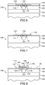
- a method of making the quantum device 100 according to the first embodiment is described below in connection with the figures 3 to 9 .
- the device 100 is made from a semiconductor layer which, in the embodiment described here, corresponds to the surface layer of a substrate of the semiconductor-on-insulator type, and more particularly of the SOI type ( “Silicon-On-Insulator” in English, or silicon on insulator).
- the semiconductor layer here comprises silicon and is arranged on a buried dielectric layer 146, or BOX (“Buried Oxide”) of the SOI substrate comprising SiO 2 .
- BOX Buried Oxide
- the buried dielectric layer 146 is placed on a substrate layer 148 serving as a support and here comprising silicon.
- the semiconductor layer is etched in order to obtain the portion 102 corresponding to the remaining portion of the semiconductor layer after this etching.
- a first etching mask comprising for example a resin, is deposited on the semiconductor layer, then lithography and etching are implemented so that the remaining portion of semiconductor corresponds to the portion 102 in which the quantum dots and tunnel barriers of device 100 will be made. The first etching mask is then removed.
- a stack of layers of materials intended for the production of the first electrostatic control gate(s) 107 is then formed by covering the first face 112 of the portion 102 and the parts of the dielectric layer 146 not covered by the portion 102.
- This stack comprises at least one dielectric layer intended for the production of the first gate dielectric(s) 110, and at least one electrically conductive layer intended for the production of the first portion(s) of electrically conductive material 108.
- a hard mask layer corresponding for example to a layer of SiN with a thickness equal to 30 nm, is deposited on this stack.
- the dielectric layer of the stack is obtained by implementing thermal oxidation of the first face 112 of the portion 102.
- a second etching mask is then deposited on the hard mask layer, the pattern of which corresponds to that of the first electrostatic control gate(s) 107 to be produced.
- the hard mask layer and the stack of layers of materials intended for the production of the first electrostatic control gate(s) 107 are then subjected to lithography and etching according to the pattern of the second etching mask.
- the remaining portions of these layers correspond to the first portion(s) of electrically conductive material 108 and to the first gate dielectric(s) 110.
- the stopping of this etching can be defined by the dielectric layer 146 serving in this case as a layer of burning stop.
- the production of the first electrostatic control gate(s) 107 defines the locations, in the portion 102, of the first region(s) 104 intended to form the quantum dots and which correspond to the region(s) of the portion 102 covered by the first electrostatic control gates 107.
- the first dielectric layer 136 comprising for example semiconductor nitride such as silicon nitride, is deposited on the structure produced, by covering the first electrostatic control grid(s) 107, the parts of the portion 102 not covered by the first electrostatic control grid(s) 107 as well as any parts of the dielectric layer 146 not covered by the portion 102 and by the first electrostatic control gate(s) 107.
- semiconductor nitride such as silicon nitride
- the structure obtained at this stage of the process is represented on the picture 3 .
- a dielectric layer 150 is then deposited covering the first dielectric layer 136, then planarized.
- the structure produced is turned over and attached to a second substrate corresponding to the substrate 142.
- this attachment is achieved by direct bonding or molecular bonding between the dielectric layer 150 and another dielectric layer 152, comprising by example of the semiconductor oxide, formed on one face of the substrate 142.
- the dielectric layers 150 and 152 together form the dielectric layer 140 previously described in connection with the figure 1 and 2 .
- the layer 148 of the first substrate is then removed, for example by mechanical abrasion and chemical attack selective with respect to the material of the buried dielectric layer 146.
- a TMAH solution can be used for this selective etching.
- the buried dielectric layer 146 is then removed, the first dielectric layer 136 being used here as an etching stop layer for this removal. This removal reveals the second face 118 of the portion 102.
- a step of lithography of a masking layer is in this case implemented, prior to the ion implantation, to mask the portions of the portion 102 which are not intended to be doped.
- the second electrostatic control gates 109 are then produced on the second face 118 of the portion 102, defining the locations of the second regions 106 of the portion 102.
- the second electrostatic control gates 109 are then covered by the second dielectric layer 138, comprising for example a dielectric material similar to that of the first dielectric layer 136.
- the device 100 is then completed, on the figure 9 , by producing the electrical interconnection level(s) 144 as well as the electrical contacts 130, 132 and 134.
- the device 100 obtained corresponds to that previously described in connection with the figure 1 and 2 .
- the doping of the third regions 120 is carried out between the deposition of the second dielectric layer 138 and the production of the electrical interconnection level(s) 144, by ion implantation or by epitaxial growth. doped in situ.
- a lithography step is in this case implemented, prior to the ion implantation or the epitaxial growth, to etch parts of the second dielectric layer 138 covering the third regions 120 and thus make the third regions 120 accessible.
- a quantum device 100 with spin qubits according to a variant of the first embodiment is described below in connection with the figure 10 which corresponds to a top view of the device 100.
- the quantum dots are not made in a semiconductor nanowire, but in a semiconductor portion 102 corresponding to a semiconductor layer.
- first electrostatic control gates controlling the minimum potential energy levels of the quantum dots
- other first electrostatic control gates are arranged in the form of columns which bear the reference 156 also controlling the minimum levels of potential energy of the quantum dots and which are superimposed on the rows 154 of first grids at the intersections between the rows and columns 154, 156 of first electrostatic control grids.
- rows and columns 154, 156 of first electrostatic control gates are represented by dotted lines because they are arranged under the semiconductor layer, on the side of the first face 112 of this layer which is not visible on the figure 10 .
- second electrostatic control grids controlling the maximum levels of potential energy of the tunnel barriers, are arranged in the form of rows and carry the reference 158, and other second electrostatic control grids are arranged in the form of columns which carry the reference 160 and which are superimposed on the rows of second gates 158 at the intersections between the rows and columns 158, 160 of second electrostatic control gates.
- the rows and columns 158, 160 of second electrostatic control gates are arranged under the semiconductor layer, on the side of the second face 118 of this layer.
- the quantum dots are arranged forming a first two-dimensional array in the semiconductor portion 102 and the tunnel barriers are arranged forming a second two-dimensional array in the semiconductor portion 102.
- the quantum dots are located at the intersections of the first control gates 154, 156 and are surrounded by tunnel barriers located under the second gates 158, 160. rows and columns of grids 154, 156, 158, 160.
- the device 100 previously described according to the different embodiments and variants can be used in a mode of operation similar to that of one or more series-coupled field-effect transistors, and operated in a cryogenic environment, i.e. i.e. in a cryostat at cryogenic temperatures (below 1 K, or even below 4 K).
- the electrostatic control gates 107, 109 are used like conventional transistor gates, the biases of which control the conductance between the third regions 120 of the structure.
- the gates located in the vicinity of one of the faces 112 or 118 are statically biased in order to control and adjust the threshold voltage(s) of the transistor(s) comprising the gates located in the vicinity of the other face, respectively 118 or 112.
Landscapes
- Junction Field-Effect Transistors (AREA)
- Engineering & Computer Science (AREA)
- Manufacturing & Machinery (AREA)
- Metal-Oxide And Bipolar Metal-Oxide Semiconductor Integrated Circuits (AREA)
- Non-Volatile Memory (AREA)
- Semiconductor Memories (AREA)
Applications Claiming Priority (1)
| Application Number | Priority Date | Filing Date | Title |
|---|---|---|---|
| FR2100454A FR3118961A1 (fr) | 2021-01-18 | 2021-01-18 | Dispositif comprenant des grilles de commande électrostatique reparties sur deux faces opposées d’une portion de semi-conducteur |
Publications (1)
| Publication Number | Publication Date |
|---|---|
| EP4033540A1 true EP4033540A1 (de) | 2022-07-27 |
Family
ID=74871639
Family Applications (1)
| Application Number | Title | Priority Date | Filing Date |
|---|---|---|---|
| EP22151813.7A Pending EP4033540A1 (de) | 2021-01-18 | 2022-01-17 | Vorrichtung mit elektrostatischen steuergates, die auf zwei gegenüberliegenden seiten eines halbleiterabschnitts verteilt sind |
Country Status (3)
| Country | Link |
|---|---|
| US (1) | US12356676B2 (de) |
| EP (1) | EP4033540A1 (de) |
| FR (1) | FR3118961A1 (de) |
Families Citing this family (2)
| Publication number | Priority date | Publication date | Assignee | Title |
|---|---|---|---|---|
| FR3114444B1 (fr) * | 2020-09-21 | 2022-09-30 | Commissariat Energie Atomique | Puce à routage bifonctionnel et procédé de fabrication associé |
| FR3161295A1 (fr) * | 2024-04-10 | 2025-10-17 | Commissariat A L'energie Atomique Et Aux Energies Alternatives | Dispositif a matrice de boites quantiques et de regions de couplage |
Citations (4)
| Publication number | Priority date | Publication date | Assignee | Title |
|---|---|---|---|---|
| US20130087766A1 (en) * | 2011-10-07 | 2013-04-11 | The Regents Of The University Of California | Scalable quantum computer architecture with coupled donor-quantum dot qubits |
| WO2017213647A1 (en) * | 2016-06-09 | 2017-12-14 | Intel Corporation | Quantum dot devices with back gates |
| WO2018063203A1 (en) * | 2016-09-29 | 2018-04-05 | Intel Corporation | Strained quantum dot devices |
| US20200185512A1 (en) * | 2018-12-05 | 2020-06-11 | The Governing Council Of The University Of Toronto | Monolithic qubit integrated circuits |
Family Cites Families (2)
| Publication number | Priority date | Publication date | Assignee | Title |
|---|---|---|---|---|
| FR3033665B1 (fr) * | 2015-03-11 | 2018-10-12 | Commissariat A L'energie Atomique Et Aux Energies Alternatives | Transistor a electron unique et son procede de realisation |
| WO2018057027A1 (en) * | 2016-09-26 | 2018-03-29 | Intel Corporation | Quantum dot devices with strained gates |
-
2021
- 2021-01-18 FR FR2100454A patent/FR3118961A1/fr active Pending
-
2022
- 2022-01-17 EP EP22151813.7A patent/EP4033540A1/de active Pending
- 2022-01-18 US US17/577,551 patent/US12356676B2/en active Active
Patent Citations (4)
| Publication number | Priority date | Publication date | Assignee | Title |
|---|---|---|---|---|
| US20130087766A1 (en) * | 2011-10-07 | 2013-04-11 | The Regents Of The University Of California | Scalable quantum computer architecture with coupled donor-quantum dot qubits |
| WO2017213647A1 (en) * | 2016-06-09 | 2017-12-14 | Intel Corporation | Quantum dot devices with back gates |
| WO2018063203A1 (en) * | 2016-09-29 | 2018-04-05 | Intel Corporation | Strained quantum dot devices |
| US20200185512A1 (en) * | 2018-12-05 | 2020-06-11 | The Governing Council Of The University Of Toronto | Monolithic qubit integrated circuits |
Non-Patent Citations (2)
| Title |
|---|
| C. H. YANG ET AL.: "Dynamically controlled charge sensing of a few-electron silicon quantum dot", AIP ADVANCES, vol. 1, 2011, pages 042111 |
| S. DE FRANCESCHI ET AL.: "SOI technology for quantum information processing", 2016 IEEE INTERNATIONAL ELECTRON DEVICES MEETING (IEDM, 2016 |
Also Published As
| Publication number | Publication date |
|---|---|
| US12356676B2 (en) | 2025-07-08 |
| FR3118961A1 (fr) | 2022-07-22 |
| US20220271151A1 (en) | 2022-08-25 |
Similar Documents
| Publication | Publication Date | Title |
|---|---|---|
| EP3401848B1 (de) | Quantenvorrichtung mit spin-qubits | |
| FR3086456A1 (fr) | Procede de realisation de transistors superposes | |
| EP3701567B1 (de) | Verfahren zur herstellung eines elektronischen bauteils mit doppelquantenpunkten | |
| FR3016237A1 (fr) | Dispositif a nanofils de semi-conducteur partiellement entoures par une grille | |
| EP1947686A2 (de) | SOI-MOSFET Vorrichtung | |
| EP2562802B1 (de) | Verfahren zur Herstellung eines dreidimensionalen integrierten Schaltkreises | |
| EP4060748B1 (de) | Vorrichtung mit zwei übereinanderliegenden ebenen von elektrostatischen steuergittern | |
| FR3081155A1 (fr) | Procede de fabrication d'un composant electronique a multiples ilots quantiques | |
| FR3033665A1 (fr) | Transistor a electron unique et son procede de realisation | |
| FR3081154A1 (fr) | Procede de fabrication d'un composant electronique a multiples ilots quantiques | |
| FR3078441A1 (fr) | Dispositif quantique comprenant des transistors fet et des qubits co-integres sur un meme substrat | |
| EP3473592B1 (de) | Quantenvorrichtung mit modulierbar gekoppelten spin-qubits | |
| FR3118961A1 (fr) | Dispositif comprenant des grilles de commande électrostatique reparties sur deux faces opposées d’une portion de semi-conducteur | |
| WO2008155379A2 (fr) | Transistor a effet de champ a contacts electriques alternes | |
| EP3660921A1 (de) | Verfahren zur herstellung eines elektronischen bauteils mit mehreren quantum dots, sowie resultierendes elektronisches bauteil | |
| EP4386634A1 (de) | Austauschelektroden für quanteninselgitter | |
| EP4391068A1 (de) | Quantenvorrichtung zur formung einer quantenpunktmatrix und herstellungsverfahren dafür | |
| FR3155634A1 (fr) | Dispositif quantique et procédé de fabrication associé | |
| EP1271657A1 (de) | Integrierte Halbleiterspeicheranordnung des DRAM-Typs und Verfahren zur Herstellung | |
| EP4554353A1 (de) | Spin qubit vorrichtung mit quantenpunkten, die in einem nanodraht durch gates gebildet werden | |
| EP4185093B1 (de) | Verfahren zur herstellung einer quantenvorrichtung | |
| EP2592663B1 (de) | Lichtemittierende Vorrichtung mit entgegengesetzten p-Typ und n-Typ Transistoren, und Herstellungsverfahren | |
| EP4554356B1 (de) | Verfahren zur herstellung einer quanten-elektronischen schaltung mit reduziertem gate-abstand | |
| EP4552160A1 (de) | Quantenvorrichtung mit halbleiter-qubits mit in einem halbleiter angeordneten gates | |
| EP4633324A1 (de) | Quantenpunkt-matrix-vorrichtung mit kopplungsbereiche, mit gates auf gegenüberliegenden seiten der quantenpunkt-matrix |
Legal Events
| Date | Code | Title | Description |
|---|---|---|---|
| PUAI | Public reference made under article 153(3) epc to a published international application that has entered the european phase |
Free format text: ORIGINAL CODE: 0009012 |
|
| STAA | Information on the status of an ep patent application or granted ep patent |
Free format text: STATUS: REQUEST FOR EXAMINATION WAS MADE |
|
| 17P | Request for examination filed |
Effective date: 20220117 |
|
| AK | Designated contracting states |
Kind code of ref document: A1 Designated state(s): AL AT BE BG CH CY CZ DE DK EE ES FI FR GB GR HR HU IE IS IT LI LT LU LV MC MK MT NL NO PL PT RO RS SE SI SK SM TR |
|
| RAP3 | Party data changed (applicant data changed or rights of an application transferred) |
Owner name: COMMISSARIAT A L'ENERGIE ATOMIQUE ET AUX ENERGIESALTERNATIVES |
|
| STAA | Information on the status of an ep patent application or granted ep patent |
Free format text: STATUS: EXAMINATION IS IN PROGRESS |
|
| 17Q | First examination report despatched |
Effective date: 20241218 |