EP4038656B1 - Détermination d'une énergie ionique optimale pour le traitement plasma d'un substrat diélectrique - Google Patents
Détermination d'une énergie ionique optimale pour le traitement plasma d'un substrat diélectrique Download PDFInfo
- Publication number
- EP4038656B1 EP4038656B1 EP20780233.1A EP20780233A EP4038656B1 EP 4038656 B1 EP4038656 B1 EP 4038656B1 EP 20780233 A EP20780233 A EP 20780233A EP 4038656 B1 EP4038656 B1 EP 4038656B1
- Authority
- EP
- European Patent Office
- Prior art keywords
- voltage
- pulses
- coefficient
- voltage slope
- slope
- Prior art date
- Legal status (The legal status is an assumption and is not a legal conclusion. Google has not performed a legal analysis and makes no representation as to the accuracy of the status listed.)
- Active
Links
Images



Classifications
-
- H—ELECTRICITY
- H01—ELECTRIC ELEMENTS
- H01J—ELECTRIC DISCHARGE TUBES OR DISCHARGE LAMPS
- H01J37/00—Discharge tubes with provision for introducing objects or material to be exposed to the discharge, e.g. for the purpose of examination or processing thereof
- H01J37/32—Gas-filled discharge tubes
- H01J37/32917—Plasma diagnostics
-
- H—ELECTRICITY
- H01—ELECTRIC ELEMENTS
- H01J—ELECTRIC DISCHARGE TUBES OR DISCHARGE LAMPS
- H01J37/00—Discharge tubes with provision for introducing objects or material to be exposed to the discharge, e.g. for the purpose of examination or processing thereof
- H01J37/32—Gas-filled discharge tubes
- H01J37/32009—Arrangements for generation of plasma specially adapted for examination or treatment of objects, e.g. plasma sources
- H01J37/32082—Radio frequency generated discharge
- H01J37/32137—Radio frequency generated discharge controlling of the discharge by modulation of energy
- H01J37/32146—Amplitude modulation, includes pulsing
-
- C—CHEMISTRY; METALLURGY
- C23—COATING METALLIC MATERIAL; COATING MATERIAL WITH METALLIC MATERIAL; CHEMICAL SURFACE TREATMENT; DIFFUSION TREATMENT OF METALLIC MATERIAL; COATING BY VACUUM EVAPORATION, BY SPUTTERING, BY ION IMPLANTATION OR BY CHEMICAL VAPOUR DEPOSITION, IN GENERAL; INHIBITING CORROSION OF METALLIC MATERIAL OR INCRUSTATION IN GENERAL
- C23C—COATING METALLIC MATERIAL; COATING MATERIAL WITH METALLIC MATERIAL; SURFACE TREATMENT OF METALLIC MATERIAL BY DIFFUSION INTO THE SURFACE, BY CHEMICAL CONVERSION OR SUBSTITUTION; COATING BY VACUUM EVAPORATION, BY SPUTTERING, BY ION IMPLANTATION OR BY CHEMICAL VAPOUR DEPOSITION, IN GENERAL
- C23C16/00—Chemical coating by decomposition of gaseous compounds, without leaving reaction products of surface material in the coating, i.e. chemical vapour deposition [CVD] processes
- C23C16/44—Chemical coating by decomposition of gaseous compounds, without leaving reaction products of surface material in the coating, i.e. chemical vapour deposition [CVD] processes characterised by the method of coating
- C23C16/458—Chemical coating by decomposition of gaseous compounds, without leaving reaction products of surface material in the coating, i.e. chemical vapour deposition [CVD] processes characterised by the method of coating characterised by the method used for supporting substrates in the reaction chamber
- C23C16/4582—Rigid and flat substrates, e.g. plates or discs
- C23C16/4583—Rigid and flat substrates, e.g. plates or discs the substrate being supported substantially horizontally
- C23C16/4586—Elements in the interior of the support, e.g. electrodes, heating or cooling devices
-
- C—CHEMISTRY; METALLURGY
- C23—COATING METALLIC MATERIAL; COATING MATERIAL WITH METALLIC MATERIAL; CHEMICAL SURFACE TREATMENT; DIFFUSION TREATMENT OF METALLIC MATERIAL; COATING BY VACUUM EVAPORATION, BY SPUTTERING, BY ION IMPLANTATION OR BY CHEMICAL VAPOUR DEPOSITION, IN GENERAL; INHIBITING CORROSION OF METALLIC MATERIAL OR INCRUSTATION IN GENERAL
- C23C—COATING METALLIC MATERIAL; COATING MATERIAL WITH METALLIC MATERIAL; SURFACE TREATMENT OF METALLIC MATERIAL BY DIFFUSION INTO THE SURFACE, BY CHEMICAL CONVERSION OR SUBSTITUTION; COATING BY VACUUM EVAPORATION, BY SPUTTERING, BY ION IMPLANTATION OR BY CHEMICAL VAPOUR DEPOSITION, IN GENERAL
- C23C16/00—Chemical coating by decomposition of gaseous compounds, without leaving reaction products of surface material in the coating, i.e. chemical vapour deposition [CVD] processes
- C23C16/44—Chemical coating by decomposition of gaseous compounds, without leaving reaction products of surface material in the coating, i.e. chemical vapour deposition [CVD] processes characterised by the method of coating
- C23C16/50—Chemical coating by decomposition of gaseous compounds, without leaving reaction products of surface material in the coating, i.e. chemical vapour deposition [CVD] processes characterised by the method of coating using electric discharges
-
- C—CHEMISTRY; METALLURGY
- C23—COATING METALLIC MATERIAL; COATING MATERIAL WITH METALLIC MATERIAL; CHEMICAL SURFACE TREATMENT; DIFFUSION TREATMENT OF METALLIC MATERIAL; COATING BY VACUUM EVAPORATION, BY SPUTTERING, BY ION IMPLANTATION OR BY CHEMICAL VAPOUR DEPOSITION, IN GENERAL; INHIBITING CORROSION OF METALLIC MATERIAL OR INCRUSTATION IN GENERAL
- C23C—COATING METALLIC MATERIAL; COATING MATERIAL WITH METALLIC MATERIAL; SURFACE TREATMENT OF METALLIC MATERIAL BY DIFFUSION INTO THE SURFACE, BY CHEMICAL CONVERSION OR SUBSTITUTION; COATING BY VACUUM EVAPORATION, BY SPUTTERING, BY ION IMPLANTATION OR BY CHEMICAL VAPOUR DEPOSITION, IN GENERAL
- C23C16/00—Chemical coating by decomposition of gaseous compounds, without leaving reaction products of surface material in the coating, i.e. chemical vapour deposition [CVD] processes
- C23C16/44—Chemical coating by decomposition of gaseous compounds, without leaving reaction products of surface material in the coating, i.e. chemical vapour deposition [CVD] processes characterised by the method of coating
- C23C16/50—Chemical coating by decomposition of gaseous compounds, without leaving reaction products of surface material in the coating, i.e. chemical vapour deposition [CVD] processes characterised by the method of coating using electric discharges
- C23C16/515—Chemical coating by decomposition of gaseous compounds, without leaving reaction products of surface material in the coating, i.e. chemical vapour deposition [CVD] processes characterised by the method of coating using electric discharges using pulsed discharges
-
- C—CHEMISTRY; METALLURGY
- C23—COATING METALLIC MATERIAL; COATING MATERIAL WITH METALLIC MATERIAL; CHEMICAL SURFACE TREATMENT; DIFFUSION TREATMENT OF METALLIC MATERIAL; COATING BY VACUUM EVAPORATION, BY SPUTTERING, BY ION IMPLANTATION OR BY CHEMICAL VAPOUR DEPOSITION, IN GENERAL; INHIBITING CORROSION OF METALLIC MATERIAL OR INCRUSTATION IN GENERAL
- C23C—COATING METALLIC MATERIAL; COATING MATERIAL WITH METALLIC MATERIAL; SURFACE TREATMENT OF METALLIC MATERIAL BY DIFFUSION INTO THE SURFACE, BY CHEMICAL CONVERSION OR SUBSTITUTION; COATING BY VACUUM EVAPORATION, BY SPUTTERING, BY ION IMPLANTATION OR BY CHEMICAL VAPOUR DEPOSITION, IN GENERAL
- C23C16/00—Chemical coating by decomposition of gaseous compounds, without leaving reaction products of surface material in the coating, i.e. chemical vapour deposition [CVD] processes
- C23C16/44—Chemical coating by decomposition of gaseous compounds, without leaving reaction products of surface material in the coating, i.e. chemical vapour deposition [CVD] processes characterised by the method of coating
- C23C16/52—Controlling or regulating the coating process
-
- G—PHYSICS
- G01—MEASURING; TESTING
- G01R—MEASURING ELECTRIC VARIABLES; MEASURING MAGNETIC VARIABLES
- G01R19/00—Arrangements for measuring currents or voltages or for indicating presence or sign thereof
- G01R19/0046—Arrangements for measuring currents or voltages or for indicating presence or sign thereof characterised by a specific application or detail not covered by any other subgroup of G01R19/00
-
- H—ELECTRICITY
- H01—ELECTRIC ELEMENTS
- H01J—ELECTRIC DISCHARGE TUBES OR DISCHARGE LAMPS
- H01J37/00—Discharge tubes with provision for introducing objects or material to be exposed to the discharge, e.g. for the purpose of examination or processing thereof
- H01J37/32—Gas-filled discharge tubes
- H01J37/32009—Arrangements for generation of plasma specially adapted for examination or treatment of objects, e.g. plasma sources
- H01J37/32082—Radio frequency generated discharge
- H01J37/32174—Circuits specially adapted for controlling the RF discharge
-
- H—ELECTRICITY
- H01—ELECTRIC ELEMENTS
- H01J—ELECTRIC DISCHARGE TUBES OR DISCHARGE LAMPS
- H01J37/00—Discharge tubes with provision for introducing objects or material to be exposed to the discharge, e.g. for the purpose of examination or processing thereof
- H01J37/32—Gas-filled discharge tubes
- H01J37/32431—Constructional details of the reactor
- H01J37/32532—Electrodes
- H01J37/32577—Electrical connecting means
-
- H—ELECTRICITY
- H01—ELECTRIC ELEMENTS
- H01J—ELECTRIC DISCHARGE TUBES OR DISCHARGE LAMPS
- H01J37/00—Discharge tubes with provision for introducing objects or material to be exposed to the discharge, e.g. for the purpose of examination or processing thereof
- H01J37/32—Gas-filled discharge tubes
- H01J37/32431—Constructional details of the reactor
- H01J37/32715—Workpiece holder
-
- H—ELECTRICITY
- H10—SEMICONDUCTOR DEVICES; ELECTRIC SOLID-STATE DEVICES NOT OTHERWISE PROVIDED FOR
- H10P—GENERIC PROCESSES OR APPARATUS FOR THE MANUFACTURE OR TREATMENT OF DEVICES COVERED BY CLASS H10
- H10P50/00—Etching of wafers, substrates or parts of devices
- H10P50/20—Dry etching; Plasma etching; Reactive-ion etching
- H10P50/24—Dry etching; Plasma etching; Reactive-ion etching of semiconductor materials
- H10P50/242—Dry etching; Plasma etching; Reactive-ion etching of semiconductor materials of Group IV materials
-
- H—ELECTRICITY
- H10—SEMICONDUCTOR DEVICES; ELECTRIC SOLID-STATE DEVICES NOT OTHERWISE PROVIDED FOR
- H10P—GENERIC PROCESSES OR APPARATUS FOR THE MANUFACTURE OR TREATMENT OF DEVICES COVERED BY CLASS H10
- H10P95/00—Generic processes or apparatus for manufacture or treatments not covered by the other groups of this subclass
-
- H—ELECTRICITY
- H01—ELECTRIC ELEMENTS
- H01J—ELECTRIC DISCHARGE TUBES OR DISCHARGE LAMPS
- H01J2237/00—Discharge tubes exposing object to beam, e.g. for analysis treatment, etching, imaging
- H01J2237/245—Detection characterised by the variable being measured
- H01J2237/24564—Measurements of electric or magnetic variables, e.g. voltage, current, frequency
-
- H—ELECTRICITY
- H01—ELECTRIC ELEMENTS
- H01J—ELECTRIC DISCHARGE TUBES OR DISCHARGE LAMPS
- H01J2237/00—Discharge tubes exposing object to beam, e.g. for analysis treatment, etching, imaging
- H01J2237/32—Processing objects by plasma generation
- H01J2237/33—Processing objects by plasma generation characterised by the type of processing
- H01J2237/332—Coating
-
- H—ELECTRICITY
- H01—ELECTRIC ELEMENTS
- H01J—ELECTRIC DISCHARGE TUBES OR DISCHARGE LAMPS
- H01J2237/00—Discharge tubes exposing object to beam, e.g. for analysis treatment, etching, imaging
- H01J2237/32—Processing objects by plasma generation
- H01J2237/33—Processing objects by plasma generation characterised by the type of processing
- H01J2237/334—Etching
- H01J2237/3341—Reactive etching
Definitions
- the present invention is related to a method and an apparatus for plasma processing of dielectric substrates, such as plasma-assisted etching and deposition.
- the present invention is related to a method of determining an optimal ion energy for plasma processing of dielectric substrates, and to the corresponding apparatus.
- Plasma-assisted etching and deposition such as reactive ion etching (RIE), atomic layer etching (ALE) and atomic layer deposition (ALD), are widely used in semiconductor manufacturing.
- RIE reactive ion etching
- ALE atomic layer etching
- ALD atomic layer deposition
- plasma is used not only to increase the rate of removing or growing materials, but also to increase the quality of the process.
- the plasma consists of positive ions, negative electrons and neutral particles.
- the ions are accelerated by the negative voltage potential on the material surface and bombard the material, so as to supply additional energy to the surface and accelerate the chemical reactions.
- the normal direction of ion bombardment to the material surface also enhances the anisotropy of the etching.
- the ion energy is controlled within a limited range. Ions with too low energy result in a slow reaction rate while ions with too high energy causes sputtering, which decreases the selectivity. With the increasing demands on the smaller semiconductor size, accurate control of ion energy becomes critical in both plasma-enhanced deposition and etching. In general, a narrow ion energy distribution (IED) falling into a certain range of energy value is desired, which requires a constant negative voltage potential on the substrate material surface.
- IED narrow ion energy distribution
- the ion energy is determined by the voltage potential of the substrate surface.
- a negative dc bias voltage can be directly connected to the table in the reactor. By varying the dc value of the voltage, the energy of the ions can be controlled correspondingly.
- there is an equivalent substrate capacitance for a dielectric substrate material, there is an equivalent substrate capacitance.
- a simple dc bias does not work well because the ions are charging the substrate during etching, resulting in an increase to the substrate voltage potential.
- a radiofrequency (RF) sinusoidal bias voltage is usually used in the conventional reactor.
- a blocking capacitor is required for RF biasing in order to generate a self-biased negative dc potential on the sheath.
- the sinusoidal voltage waveform produces a variant voltage potential on the substrate surface, thus resulting in a wide and bimodal lED.
- increasing the frequency helps narrowing the IED, it is limited by the ion mass and it is much less effective for light ions such as hydrogen.
- a sufficiently large biasing frequency makes the RF wavelength comparable to the substrate dimension, causing severe nonuniformities.
- the RF biasing generates a lot of reactive power, leading to a low efficiency and high cost.
- the pulse-shape biasing is also used in plasma-enhanced etching and deposition. It consists of a wide negative pulse in the deposition and etching phase and a short positive pulse during the discharge phase.
- the positive pulse is applied to the substrate potential in order to attract electrons and discharge the accumulated ions periodically.
- the substrate potential is still charged by the ions during etching or deposition phase, thereby a narrow lED cannot be obtained with this simple waveform.
- RF biasing although increasing the frequency is effective in narrowing the IED under certain circumstances, it degrades the process quality.
- the bias voltage waveform consists of a decreasing negative voltage slope to compensate the substrate potential rise during deposition and etching phase, and a positive voltage pulse to attract electrons to keep charge balance during discharge phase.
- Such a voltage waveform can produce a narrow ion energy distribution.
- the repetition frequency is much less than the traditional RF biasing and pulse-shape biasing.
- the negative voltage slope in US 2014/061156 A1 can be obtained by incorporating an ion current compensation, such as a current source, to a switch-mode power supply coupled to the substrate.
- the negative voltage slope of the pulsed voltage waveform must be finely tuned in order to obtain the narrowest lED.
- US 2014/061156 A1 proposes to evaluate a function based on the voltage slope, the effective capacitance of the substrate and the ion current compensation, and to adjust the ion current compensation until the function is true which would correspond to the narrowest lED. The function is made to be true when the ion current compensation equals the ion current.
- a first ion current compensation is applied for a first cycle and a first voltage slope of the pulsed voltage waveform is measured.
- a second ion current compensation for a second cycle is applied and a second voltage slope is measured. From this, a third ion current compensation can be determined at which the function is expected to be true and therefore would result in a narrow lED.
- the plasma sheath (also simply referred to as sheath) is a layer in a plasma near the substrate surface and possibly the walls of the plasma processing chamber with a high density of positive ions and thus an overall excess of positive charge.
- the surface with which the sheath is in contact with typically has a preponderance of negative charge.
- the sheath arises by virtue of the faster velocity of electrons than positive ions thus causing a greater proportion of electrons to reach the substrate surface or walls, thus decreasing the density of electrons in the sheath.
- US 2017/358431 A1 A1 discloses a system and a method for controlling a voltage waveform at a substrate during plasma processing, including applying a shaped pulse bias waveform to a substrate support and further including capturing a voltage representative of a voltage at a substrate positioned on the substrate support surface and iteratively adjusting the shaped pulse bias waveform based on the captured signal.
- a method of determining an ion energy for plasma processing of a dielectric substrate as set out in claim 1 and its dependent claims.
- the method according to the invention comprises exposing the dielectric substrate to a plasma discharge and applying a pulsed voltage waveform generated by a power supply to the dielectric substrate, particularly during the exposure.
- the pulsed voltage waveform comprises a sequence of pulses, each pulse comprising a higher, e.g. positive, voltage interval and a lower, e.g. negative, voltage interval, wherein the lower voltage interval comprises a voltage slope, in particular a negative voltage slope.
- the sequence comprises first pulses having differing voltage slopes between one another.
- the first pulses are applied to the dielectric substrate, in particular during exposure to the plasma discharge.
- the voltage slope and an output current corresponding to the voltage slope at an output of the power supply are determined. Either one or both of the voltage slope and corresponding output current can be measured, and the other one can be set by a control unit coupled to the power supply.
- At least one coefficient of a mathematical relation between the voltage slope and the corresponding output current is determined based solely on the voltage slope and the output current determined for one or more of the first pulses.
- the mathematical relation is a function expressing a relation between the voltage slope and the output current. Either one of the voltage slope and the output current can be a variable of the function, and evaluating the function for the variable yields the other one of the voltage slope and output current.
- the function comprises at least one coefficient, which can be variable with the voltage slope and/or the output current. According to the invention, the mathematical relation (function) is resolved for the at least one coefficient, such that the at least one coefficient is determined based on known (determined) values of voltage slope and output current.
- a test function can be applied to the at least one coefficient in order to determine an optimal voltage slope.
- the test function is true when the at least one coefficient relates to an optimal voltage slope making the lED narrowest.
- the test function advantageously finds an extremum of the at least one coefficient.
- the method of the invention allows to tune the operational parameters of the plasma processing apparatus in a fully automated way, without manual intervention, and without requiring time consuming or cumbersome measurements of other electrical quantities, such as capacitance, which reduces cost and throughput time. Additionally, the automated tuning according to the invention allows to auto-tune every dielectric substrate that is processed, leading to higher accuracy. Typically, a sequence of between 10 and 50 first pulses would suffice in order to find an optimal voltage slope with satisfactory accuracy.
- the at least one coefficient is advantageously related to the system capacitances.
- the coefficient(s) By evaluating the coefficient(s) based on the voltage and current values only, the voltage-dependent and/or current-dependent behaviour of the system capacitances are implicitly taken into account and there is no need to measure them separately.
- the method according to the invention therefore can provide a more accurate tuning to a desired (e.g., narrowest) lED.
- the mathematical relation is a polynomial function between the output current and the voltage slope.
- the polynomial function can be of any degree, e.g. zero, one, two, three, etc., depending on the equivalent electrical model of the plasma processing system.
- the first pulses can form a sequence having monotonically increasing voltage slopes.
- the method may start with very small, e.g. zero, voltage slope, and systematically increasing the (negative) voltage slope until an extremum (e.g. maximum value) of the at least one coefficient is found.
- the voltage slope steps between consecutive pulses can be constant, or variable, and the method may provide to automatically adapt the voltage slope step between the first pulses, e.g. based on a behaviour of the at least one coefficient that is determined. It will be convenient to note that any other suitable convergence algorithm can be used for selecting the voltage slopes in order to converge to an extremum of the at least one coefficient.
- an apparatus for plasma processing of a dielectric substrate as set out in claim 11 and its dependent claims.
- the apparatus comprises means for generating a plasma, e.g. a plasma reactor coupled to an external power supply through a matching network, a processing platform for supporting the dielectric substrate and configured for exposure to the plasma, a power supply (power amplifier), a voltage measurement device and a current measurement device.
- the plasma is excited and sustained by the external power supply.
- the power amplifier is coupled to the processing platform and to a control unit.
- the power amplifier is configured to output a configurable tailored pulse-shape voltage waveform.
- the apparatus is configured to carry out the method according to the present invention.
- the method of the invention can be implemented in the control unit.
- the method and the apparatus as described herein can also be used to calculate and dimension electrical parameters which are hard to measure directly in practice, including the substrate capacitance, the table capacitance and the ion current.
- FIG. 1 An apparatus for plasma processing a dielectric substrate, such as a semiconductor substrate, is shown in FIG. 1 .
- Gas is infused to the reactor 110.
- the plasma is ignited in the reactor 110 with an external power supply 101, which is coupled with the gas by a matching network 105 and a coil 108 outside the chamber.
- the power supply is connected to the matching network 105 and the matching network is connected to the coil 108.
- the power supply 101 can be any suitable power source including radiofrequency (RF), microwave-frequency (MF) and pulsed dc power sources.
- RF radiofrequency
- MF microwave-frequency
- pulsed dc power sources pulsed dc power sources.
- the plasma source as shown in FIG. 1 is inductively coupled, it can be of any other variety, such as capacitively coupled plasma source and helicon type plasma source.
- the apparatus of Fig. 1 can be used for plasma etching or deposition. Therefore, a dielectric substrate material 109 is placed on the table 111 inside the reactor 110. The pressure in the reactor is kept low (i.e. below atmospheric pressure) by a (vacuum) pump depicted in FIG. 1 . A power amplifier 114 is connected to the table 111 through electrical connection 113.
- a voltage measurement unit 116 can be connected to the power amplifier 114, measuring the output voltage of the amplifier.
- the voltage measurement unit 116 is coupled to controller 115 through (data) connection 117 for sending measured results to the controller 115.
- a current measurement unit 119 can be provided to measure the output current of the power amplifier 114, e.g. through an interface 112 connected to electrical connection 113 and/or table 111.
- the current measurement unit 119 is coupled to controller 115 through (data) connection 120 for sending measured results to the controller 115.
- the controller 115 implements an automatic control algorithm according to the present invention, which is based on the measured voltage and/or current values.
- the controller 115 is coupled to the power amplifier 114 through (data) connection 118 for sending control signals to the power amplifier 114 to adjust the output (voltage) waveform.
- the automatic control algorithm is configured to control ion energy in order to obtain a narrowest lED.
- the control algorithm is implemented as a real-time control system with a voltage and/or current feedback.
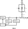
- FIG. 2 A basic equivalent electric model of the system of Fig. 1 is depicted in FIG. 2 .
- the plasma can be assumed to be a constant voltage source V p .
- An ion sheath is formed between the plasma and the surface of the material.
- the ion sheath is equivalent to a dc current source I I in parallel with a sheath capacitance C sh and a diode D 1 .
- the substrate is equivalent to a capacitor C sub .
- C sub is infinitely large, which can be treated as an ideal wire.
- C sub has a finite value.
- the table is conductive and connected to the output of the power amplifier.
- the output voltage V out is a constant dc value.
- the voltage and current measurement unit are used to monitor the dc value.
- V out is regulated by the feedback controller.
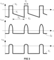
- the waveform of V out is of a tailored pulse-shape, which can be divided into 2 phases, including a discharge phase and an etching or deposition phase.
- the discharge phase consists of a positive pulse V 0 lasting for T 1 , used to attract electrons and discharge the substrate periodically. T 1 should be as short as possible only if the substrate surface gets fully discharged.
- the etching or deposition phase consists of a negative slope defined by V 1 , V 2 and T 2 .
- a negative voltage V 1 is applied to the table after the substrate is fully discharged.
- the voltage potential V e on the substrate surface during etching or deposition is approximated by V e ⁇ V 1 ⁇ V 0 .
- a negative voltage slope should be applied to the table.
- the voltage slope is defined by 3 portions V 1 , V 2 and T 2 .
- I I and C sub are unknown. In the prior arts, it is tuned either by hand or by theoretical calculation. Both tuning methods result in a deviation with the optimal voltage slope.
- the hand-tuning method requires a lot of time and an additional retarding field energy analyzer or equivalent.
- the above theoretical calculation method is based on an over-simplified model and relies on the pre-measured substrate capacitance, which might vary in the process.
- an algorithm to auto-tune the output voltage slope works based only on output voltage and output current. Either one can be set, e.g. by controller 115 and the other one can be measured, e.g. by voltage measurement unit 116 and/or current measurement unit 119.
- the tuning algorithm according to the invention can be implemented by the controller 115 in a fully automatic way and discards the need for any manual intervention or additional measurement (e.g. measurement of capacitance values).
- the output current is a negative dc value and equal to - I p .
- V sh turns to be constant.
- the lED can be tuned to be the narrowest.
- k ( S ) or b ( S ) can be calculated based on the real-time measurement results of the output voltage and current.
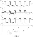
- the approximation is accurate if the step value of S n - S n- 1 is sufficiently small. As depicted by FIG.
- the above method can be also used to calculate the unknown parameters.
- the power amplifier 114 can be any variety of suitable power amplifiers. In one embodiment, it can be a voltage-source amplifier, including a switched-mode voltage amplifier, a linear amplifier or any combination of them. In another embodiment, the power amplifier can be realized by a hybrid converter.
- the hybrid converter comprises two adjustable dc voltage-source amplifiers V 0 and V 1 , two switches S 1 and S 2 and an adjustable dc current-source amplifier I P .
- the positive pulse V 0 can be obtained by turning on S 1 .
- the output voltage v out turns to be V 1 .
- the output voltage slope rate is determined by the magnitude of the I P .
- Such a hybrid converter is suitable for carrying out the tuning methods described herein. By varying the magnitude of the I P , the maximum value of k ( S ) or b ( S ) can be found as described above, allowing to obtain the narrowest lED.
- the method of the present invention is not limited to find the maximum value of k ( S ) or b ( S ) .
- the structure of a reactor might be different, resulting in a different equivalent electric model. Since the sheath capacitance is virtually removed from the electric model when the narrowest lED is obtained, an exceptional behaviour is introduced to the mathematic relations, such as an extremum, a singularity, etc. Such a behaviour can be found by applying a dedicated test function, e.g. finding the maximum of coefficients k ( S ) or b ( S ) , by varying the output voltage slope.
- the above auto-tuning method was implemented in an experiment.
- the coefficient k ( S m -1 ) , k ( S m ) , k ( S m +1 ) could be determined and a maximum k ( S ) was found to be k ( S m ).
- the dc current was changed in small steps and therefore the voltage slope difference between consecutive pulses is very small and hard to recognize from the figure. Therefore, the optimum voltage slope is S m .
- the ion energy distribution was measured for the different voltage slopes, as depicted in FIG. 7 .
- the lED corresponding to S m effectively yielded the narrowest width, thereby proving the reliability of the method of the present invention.
Landscapes
- Chemical & Material Sciences (AREA)
- Engineering & Computer Science (AREA)
- Physics & Mathematics (AREA)
- Plasma & Fusion (AREA)
- Analytical Chemistry (AREA)
- Chemical Kinetics & Catalysis (AREA)
- General Chemical & Material Sciences (AREA)
- Materials Engineering (AREA)
- Mechanical Engineering (AREA)
- Metallurgy (AREA)
- Organic Chemistry (AREA)
- General Physics & Mathematics (AREA)
- Plasma Technology (AREA)
- Drying Of Semiconductors (AREA)
- Chemical Vapour Deposition (AREA)
Claims (15)
- Procédé de détermination d'une énergie ionique pour un traitement par plasma d'un substrat diélectrique (109), le procédé comprenant les étapes ci-dessous consistant à :exposer le substrat diélectrique (109) à une décharge de plasma ;appliquer une forme d'onde de tension pulsée générée par une alimentation électrique (114) au substrat diélectrique ;dans lequel la forme d'onde de tension pulsée comprend une séquence d'impulsions, chaque impulsion comprenant un intervalle de tension supérieure et un intervalle de tension inférieure, dans lequel l'intervalle de tension inférieure comprend une pente de tension ;caractérisé en ce que le procédé comprend en outre les étapes ci-dessous consistant à :générer des premières impulsions de la séquence présentant des pentes de tension différentes les unes des autres et appliquer les premières impulsions au substrat diélectrique ;pour chacune des premières impulsions, déterminer la pente de tension (S) et un courant de sortie (IP ) correspondant à la pente de tension au niveau d'une sortie de l'alimentation électrique ;pour chacune des premières impulsions, déterminer au moins un coefficient (k, b) d'une relation mathématique entre la pente de tension et le courant de sortie correspondant uniquement sur la base de la pente de tension et du courant de sortie déterminés pour une ou plusieurs des premières impulsions ;appliquer une fonction de test audit au moins un coefficient et sélectionner une valeur de pente de tension optimale correspondante audit au moins un coefficient qui rend vraie la fonction de test.
- Procédé selon la revendication 1, dans lequel ledit au moins un coefficient est une expression constituée par : un ou plusieurs opérateurs mathématiques, une ou plusieurs valeurs des pentes de tension et une ou plusieurs valeurs du courant de sortie.
- Procédé selon la revendication 1 ou 2, dans lequel la relation mathématique est une fonction polynomiale entre le courant de sortie et la pente de tension.
- Procédé selon la revendication 3, dans lequel la fonction polynomiale est un polynôme du premier degré IP = k S + b, dans lequel « IP » représente le courant de sortie, « S » représente la pente de tension et dans lequel ledit au moins un coefficient correspond à au moins l'un parmi « k » et « b ».
- Procédé selon l'une quelconque des revendications précédentes, dans lequel ledit au moins un coefficient est représentatif d'une ou plusieurs capacités d'une interaction entre la décharge de plasma et le substrat diélectrique, ledit au moins un coefficient étant résolu uniquement sur la base de la pente de tension et du courant de sortie déterminés pour une ou plusieurs des premières impulsions.
- Procédé selon l'une quelconque des revendications précédentes, dans lequel les premières impulsions présentent des pentes de tension à croissance monotone.
- Procédé selon l'une quelconque des revendications précédentes, comprenant l'étape consistant à mesurer, pour chacune des premières impulsions, au moins l'un des éléments parmi : la pente de tension respective et le courant de sortie correspondant à la pente de tension.
- Procédé selon l'une quelconque des revendications précédentes, dans lequel la fonction de test est configurée de manière à déterminer un extremum dudit au moins un coefficient.
- Procédé selon l'une quelconque des revendications précédentes, comprenant en outre l'étape consistant à générer des secondes impulsions de la séquence, les secondes impulsions présentant une pente de tension correspondant à la valeur de pente de tension optimale et l'étape consistant à appliquer les secondes impulsions au substrat diélectrique en vue de mettre en oeuvre le traitement par plasma.
- Procédé selon l'une quelconque des revendications précédentes, dans lequel le traitement par plasma est sélectionné parmi une technique ou une combinaison des techniques ci-après : une gravure assistée par plasma et un dépôt assisté par plasma.
- Appareil pour un traitement par plasma d'un substrat diélectrique (109), comprenant :un moyen pour générer un plasma (101, 105, 108) ;une plateforme de traitement (111) destinée à soutenir le substrat diélectrique ;une alimentation électrique (114) comprenant une sortie (113) couplée à la plateforme de traitement ;au moins l'une parmi : une unité de mesure de tension (116) et une unité de mesure de courant (119) couplées à la sortie ; etune unité de commande (115) couplée à l'alimentation électrique (114), dans lequel l'unité de commande et l'alimentation électrique sont configurées conjointement de manière à générer une forme d'onde de tension pulsée, dans laquelle la forme d'onde de tension pulsée comprend une séquence d'impulsions, chaque impulsion comprenant un intervalle de tension supérieure et un intervalle de tension inférieure, dans lequel l'intervalle de tension inférieure comprend une pente de tension (S) ;caractérisé en ce que :l'unité de commande (115) et l'alimentation électrique (114) sont configurées conjointement de manière à générer des premières impulsions de la séquence présentant des pentes de tension différentes les unes des autres ;pour chacune des premières impulsions, l'unité de commande est configurée de manière à déterminer la pente de tension et le courant de sortie correspondant au niveau de la sortie, et à évaluer au moins un coefficient (k, b) d'une relation mathématique entre la pente de tension (S) et le courant de sortie (IP ), uniquement sur la base de la pente de tension et du courant de sortie déterminés pour une ou plusieurs des premières impulsions, dans laquelle l'unité de commande est en outre configurée de manière à appliquer une fonction de test audit au moins un coefficient.
- Appareil selon la revendication 11, dans lequel l'unité de commande et l'alimentation électrique sont configurées conjointement de manière à générer des secondes impulsions de la séquence, les secondes impulsions présentant une pente de tension représentative dudit au moins un coefficient qui rend vraie la fonction de test.
- Appareil selon la revendication 11 ou 12, dans lequel l'unité de commande est configurée de manière à mettre en oeuvre le procédé selon l'une quelconque des revendications 1 à 8.
- Appareil selon la revendication 13, dans lequel l'unité de commande est configurée de manière à mettre en oeuvre le procédé selon l'une quelconque des revendications 1 à 8 pour chaque substrat diélectrique traité.
- Appareil selon l'une quelconque des revendications 11 à 14, dans lequel l'alimentation électrique est un convertisseur hybride comprenant une alimentation électrique à découpage et une source de courant réglable.
Applications Claiming Priority (2)
| Application Number | Priority Date | Filing Date | Title |
|---|---|---|---|
| NL2023935A NL2023935B1 (en) | 2019-10-02 | 2019-10-02 | Determining an optimal ion energy for plasma processing of a dielectric substrate |
| PCT/EP2020/077536 WO2021064110A1 (fr) | 2019-10-02 | 2020-10-01 | Détermination d'énergie ionique optimale pour traitement au plasma de substrat diélectrique |
Publications (3)
| Publication Number | Publication Date |
|---|---|
| EP4038656A1 EP4038656A1 (fr) | 2022-08-10 |
| EP4038656B1 true EP4038656B1 (fr) | 2023-06-07 |
| EP4038656C0 EP4038656C0 (fr) | 2023-06-07 |
Family
ID=68425237
Family Applications (1)
| Application Number | Title | Priority Date | Filing Date |
|---|---|---|---|
| EP20780233.1A Active EP4038656B1 (fr) | 2019-10-02 | 2020-10-01 | Détermination d'une énergie ionique optimale pour le traitement plasma d'un substrat diélectrique |
Country Status (8)
| Country | Link |
|---|---|
| US (1) | US12347662B2 (fr) |
| EP (1) | EP4038656B1 (fr) |
| JP (1) | JP7214046B2 (fr) |
| KR (1) | KR102852168B1 (fr) |
| CN (1) | CN114556519A (fr) |
| NL (1) | NL2023935B1 (fr) |
| TW (1) | TWI805948B (fr) |
| WO (1) | WO2021064110A1 (fr) |
Families Citing this family (4)
| Publication number | Priority date | Publication date | Assignee | Title |
|---|---|---|---|---|
| US12567572B2 (en) | 2023-07-11 | 2026-03-03 | Advanced Energy Industries, Inc. | Plasma behaviors predicted by current measurements during asymmetric bias waveform application |
| KR102850760B1 (ko) * | 2024-05-09 | 2025-08-28 | 엠케이에스코리아 유한회사 | 펄스 발생기의 비대칭 멀티-레벨 제어 |
| US20260051454A1 (en) * | 2024-08-17 | 2026-02-19 | Inspiring Atoms Pte Ltd | Control System and Method for Ion Energy Distribution in Plasma Process Chambers Using Tailored Waveform Generators |
| JP7644300B1 (ja) * | 2024-09-06 | 2025-03-11 | 株式会社京三製作所 | パルス電源装置 |
Family Cites Families (22)
| Publication number | Priority date | Publication date | Assignee | Title |
|---|---|---|---|---|
| JPH09129621A (ja) | 1995-09-28 | 1997-05-16 | Applied Materials Inc | パルス波形バイアス電力 |
| US6201208B1 (en) * | 1999-11-04 | 2001-03-13 | Wisconsin Alumni Research Foundation | Method and apparatus for plasma processing with control of ion energy distribution at the substrates |
| JP4319514B2 (ja) | 2002-11-29 | 2009-08-26 | 株式会社日立ハイテクノロジーズ | サグ補償機能付き高周波電源を有するプラズマ処理装置 |
| US7851367B2 (en) * | 2006-08-31 | 2010-12-14 | Kabushiki Kaisha Toshiba | Method for plasma processing a substrate |
| JP4607930B2 (ja) * | 2007-09-14 | 2011-01-05 | 株式会社東芝 | プラズマ処理装置およびプラズマ処理方法 |
| JP5295833B2 (ja) | 2008-09-24 | 2013-09-18 | 株式会社東芝 | 基板処理装置および基板処理方法 |
| US9887069B2 (en) * | 2008-12-19 | 2018-02-06 | Lam Research Corporation | Controlling ion energy distribution in plasma processing systems |
| US9435029B2 (en) * | 2010-08-29 | 2016-09-06 | Advanced Energy Industries, Inc. | Wafer chucking system for advanced plasma ion energy processing systems |
| US11615941B2 (en) * | 2009-05-01 | 2023-03-28 | Advanced Energy Industries, Inc. | System, method, and apparatus for controlling ion energy distribution in plasma processing systems |
| US9287092B2 (en) * | 2009-05-01 | 2016-03-15 | Advanced Energy Industries, Inc. | Method and apparatus for controlling ion energy distribution |
| KR101860182B1 (ko) * | 2012-08-28 | 2018-05-21 | 어드밴스드 에너지 인더스트리즈 인코포레이티드 | 스위칭 모드 이온 에너지 분포 시스템을 제어하기 위한 방법 |
| US9685297B2 (en) * | 2012-08-28 | 2017-06-20 | Advanced Energy Industries, Inc. | Systems and methods for monitoring faults, anomalies, and other characteristics of a switched mode ion energy distribution system |
| KR101909571B1 (ko) * | 2012-08-28 | 2018-10-19 | 어드밴스드 에너지 인더스트리즈 인코포레이티드 | 넓은 다이내믹 레인지 이온 에너지 바이어스 제어; 고속 이온 에너지 스위칭; 이온 에너지 제어와 펄스동작 바이어스 서플라이; 및 가상 전면 패널 |
| CN104782233B (zh) * | 2012-08-28 | 2018-12-25 | 先进能源工业公司 | 控制开关模式离子能量分布系统的方法 |
| US9210790B2 (en) * | 2012-08-28 | 2015-12-08 | Advanced Energy Industries, Inc. | Systems and methods for calibrating a switched mode ion energy distribution system |
| US12456611B2 (en) * | 2016-06-13 | 2025-10-28 | Applied Materials, Inc. | Systems and methods for controlling a voltage waveform at a substrate during plasma processing |
| KR102476353B1 (ko) * | 2016-07-26 | 2022-12-09 | 삼성전자주식회사 | 반도체 설비의 설정 파형 발생기, 플라즈마 처리 장치, 플라즈마 처리 장치의 제어 방법 및 반도체 장치의 제조 방법 |
| US10312048B2 (en) * | 2016-12-12 | 2019-06-04 | Applied Materials, Inc. | Creating ion energy distribution functions (IEDF) |
| WO2019099870A1 (fr) * | 2017-11-17 | 2019-05-23 | Advanced Energy Industries, Inc. | Émission d'impulsions de source de traitement par plasma et polarisation de substrat synchronisées |
| KR102592922B1 (ko) * | 2018-06-21 | 2023-10-23 | 삼성전자주식회사 | 기판 처리 장치, 신호 소스 장치, 물질막의 처리 방법, 및 반도체 소자의 제조 방법 |
| CN118315254A (zh) * | 2019-01-22 | 2024-07-09 | 应用材料公司 | 用于控制脉冲电压波形的反馈回路 |
| TW202536923A (zh) * | 2019-07-12 | 2025-09-16 | 新加坡商Aes 全球公司 | 具有控制開關之偏壓供應器 |
-
2019
- 2019-10-02 NL NL2023935A patent/NL2023935B1/en not_active IP Right Cessation
-
2020
- 2020-09-30 TW TW109134066A patent/TWI805948B/zh active
- 2020-10-01 KR KR1020227014710A patent/KR102852168B1/ko active Active
- 2020-10-01 CN CN202080070215.4A patent/CN114556519A/zh active Pending
- 2020-10-01 EP EP20780233.1A patent/EP4038656B1/fr active Active
- 2020-10-01 WO PCT/EP2020/077536 patent/WO2021064110A1/fr not_active Ceased
- 2020-10-01 JP JP2022520514A patent/JP7214046B2/ja active Active
- 2020-10-01 US US17/766,373 patent/US12347662B2/en active Active
Also Published As
| Publication number | Publication date |
|---|---|
| TW202132791A (zh) | 2021-09-01 |
| US12347662B2 (en) | 2025-07-01 |
| KR102852168B1 (ko) | 2025-08-29 |
| JP7214046B2 (ja) | 2023-01-27 |
| CN114556519A (zh) | 2022-05-27 |
| NL2023935B1 (en) | 2021-05-31 |
| TWI805948B (zh) | 2023-06-21 |
| WO2021064110A1 (fr) | 2021-04-08 |
| EP4038656A1 (fr) | 2022-08-10 |
| KR20220083721A (ko) | 2022-06-20 |
| JP2022545980A (ja) | 2022-11-01 |
| US20240105430A1 (en) | 2024-03-28 |
| EP4038656C0 (fr) | 2023-06-07 |
Similar Documents
| Publication | Publication Date | Title |
|---|---|---|
| EP4038656B1 (fr) | Détermination d'une énergie ionique optimale pour le traitement plasma d'un substrat diélectrique | |
| KR101993880B1 (ko) | 플라즈마 처리 장치 | |
| EP1224684B1 (fr) | Procede et appareil permettant d'eliminer le courant de deplacement des mesures de courant dans un systeme de traitement au plasma | |
| US5543689A (en) | High frequency power source having corrected power output | |
| SG174831A1 (en) | Methods of and apparatus for measuring and controlling wafer potential in pulsed rf bias processing | |
| JP7812047B2 (ja) | プラズマ処理性能を制御するようにリアルタイムパルス測定とパルスタイミング調整を行うためのシステム及び方法 | |
| KR20230164552A (ko) | 플라즈마 시스 (sheath) 특성을 제어하기 위한 시스템들 및 방법들 | |
| US12266506B2 (en) | Scanning impedance measurement in a radio frequency plasma processing chamber | |
| US20250087462A1 (en) | Radio-frequency (rf) matching network and tuning technique | |
| WO2022010686A1 (fr) | Systèmes et procédés d'extraction d'informations de commande de processus à partir d'un système d'alimentation radiofréquence d'un système de traitement au plasma | |
| TW202422628A (zh) | 電漿蝕刻製程用的偏壓電壓定制波形之精準回饋控制 | |
| WO2024058852A1 (fr) | Bombardement de substrat avec des ions ayant une masse ciblée à l'aide d'une commande de phase de polarisation pulsée | |
| TWI920408B (zh) | 用於波形產生之方法及波形產生器 | |
| US12586768B2 (en) | Pulsed voltage compensation for plasma processing applications | |
| CN121523240A (zh) | 确定多等离子体状态工艺系统中谐振频率的以数据为导向的方法 |
Legal Events
| Date | Code | Title | Description |
|---|---|---|---|
| STAA | Information on the status of an ep patent application or granted ep patent |
Free format text: STATUS: UNKNOWN |
|
| STAA | Information on the status of an ep patent application or granted ep patent |
Free format text: STATUS: THE INTERNATIONAL PUBLICATION HAS BEEN MADE |
|
| PUAI | Public reference made under article 153(3) epc to a published international application that has entered the european phase |
Free format text: ORIGINAL CODE: 0009012 |
|
| STAA | Information on the status of an ep patent application or granted ep patent |
Free format text: STATUS: REQUEST FOR EXAMINATION WAS MADE |
|
| 17P | Request for examination filed |
Effective date: 20220425 |
|
| AK | Designated contracting states |
Kind code of ref document: A1 Designated state(s): AL AT BE BG CH CY CZ DE DK EE ES FI FR GB GR HR HU IE IS IT LI LT LU LV MC MK MT NL NO PL PT RO RS SE SI SK SM TR |
|
| GRAP | Despatch of communication of intention to grant a patent |
Free format text: ORIGINAL CODE: EPIDOSNIGR1 |
|
| STAA | Information on the status of an ep patent application or granted ep patent |
Free format text: STATUS: GRANT OF PATENT IS INTENDED |
|
| DAV | Request for validation of the european patent (deleted) | ||
| DAX | Request for extension of the european patent (deleted) | ||
| INTG | Intention to grant announced |
Effective date: 20220909 |
|
| GRAS | Grant fee paid |
Free format text: ORIGINAL CODE: EPIDOSNIGR3 |
|
| GRAA | (expected) grant |
Free format text: ORIGINAL CODE: 0009210 |
|
| STAA | Information on the status of an ep patent application or granted ep patent |
Free format text: STATUS: THE PATENT HAS BEEN GRANTED |
|
| AK | Designated contracting states |
Kind code of ref document: B1 Designated state(s): AL AT BE BG CH CY CZ DE DK EE ES FI FR GB GR HR HU IE IS IT LI LT LU LV MC MK MT NL NO PL PT RO RS SE SI SK SM TR |
|
| REG | Reference to a national code |
Ref country code: GB Ref legal event code: FG4D |
|
| REG | Reference to a national code |
Ref country code: CH Ref legal event code: EP Ref country code: AT Ref legal event code: REF Ref document number: 1577513 Country of ref document: AT Kind code of ref document: T Effective date: 20230615 |
|
| REG | Reference to a national code |
Ref country code: DE Ref legal event code: R096 Ref document number: 602020012273 Country of ref document: DE |
|
| U01 | Request for unitary effect filed |
Effective date: 20230704 |
|
| U07 | Unitary effect registered |
Designated state(s): AT BE BG DE DK EE FI FR IT LT LU LV MT NL PT SE SI Effective date: 20230719 |
|
| REG | Reference to a national code |
Ref country code: LT Ref legal event code: MG9D |
|
| U20 | Renewal fee for the european patent with unitary effect paid |
Year of fee payment: 4 Effective date: 20230920 |
|
| PG25 | Lapsed in a contracting state [announced via postgrant information from national office to epo] |
Ref country code: NO Free format text: LAPSE BECAUSE OF FAILURE TO SUBMIT A TRANSLATION OF THE DESCRIPTION OR TO PAY THE FEE WITHIN THE PRESCRIBED TIME-LIMIT Effective date: 20230907 Ref country code: ES Free format text: LAPSE BECAUSE OF FAILURE TO SUBMIT A TRANSLATION OF THE DESCRIPTION OR TO PAY THE FEE WITHIN THE PRESCRIBED TIME-LIMIT Effective date: 20230607 |
|
| PG25 | Lapsed in a contracting state [announced via postgrant information from national office to epo] |
Ref country code: RS Free format text: LAPSE BECAUSE OF FAILURE TO SUBMIT A TRANSLATION OF THE DESCRIPTION OR TO PAY THE FEE WITHIN THE PRESCRIBED TIME-LIMIT Effective date: 20230607 Ref country code: HR Free format text: LAPSE BECAUSE OF FAILURE TO SUBMIT A TRANSLATION OF THE DESCRIPTION OR TO PAY THE FEE WITHIN THE PRESCRIBED TIME-LIMIT Effective date: 20230607 Ref country code: GR Free format text: LAPSE BECAUSE OF FAILURE TO SUBMIT A TRANSLATION OF THE DESCRIPTION OR TO PAY THE FEE WITHIN THE PRESCRIBED TIME-LIMIT Effective date: 20230908 |
|
| PG25 | Lapsed in a contracting state [announced via postgrant information from national office to epo] |
Ref country code: SK Free format text: LAPSE BECAUSE OF FAILURE TO SUBMIT A TRANSLATION OF THE DESCRIPTION OR TO PAY THE FEE WITHIN THE PRESCRIBED TIME-LIMIT Effective date: 20230607 |
|
| PG25 | Lapsed in a contracting state [announced via postgrant information from national office to epo] |
Ref country code: IS Free format text: LAPSE BECAUSE OF FAILURE TO SUBMIT A TRANSLATION OF THE DESCRIPTION OR TO PAY THE FEE WITHIN THE PRESCRIBED TIME-LIMIT Effective date: 20231007 |
|
| PG25 | Lapsed in a contracting state [announced via postgrant information from national office to epo] |
Ref country code: SM Free format text: LAPSE BECAUSE OF FAILURE TO SUBMIT A TRANSLATION OF THE DESCRIPTION OR TO PAY THE FEE WITHIN THE PRESCRIBED TIME-LIMIT Effective date: 20230607 Ref country code: SK Free format text: LAPSE BECAUSE OF FAILURE TO SUBMIT A TRANSLATION OF THE DESCRIPTION OR TO PAY THE FEE WITHIN THE PRESCRIBED TIME-LIMIT Effective date: 20230607 Ref country code: RO Free format text: LAPSE BECAUSE OF FAILURE TO SUBMIT A TRANSLATION OF THE DESCRIPTION OR TO PAY THE FEE WITHIN THE PRESCRIBED TIME-LIMIT Effective date: 20230607 Ref country code: IS Free format text: LAPSE BECAUSE OF FAILURE TO SUBMIT A TRANSLATION OF THE DESCRIPTION OR TO PAY THE FEE WITHIN THE PRESCRIBED TIME-LIMIT Effective date: 20231007 Ref country code: CZ Free format text: LAPSE BECAUSE OF FAILURE TO SUBMIT A TRANSLATION OF THE DESCRIPTION OR TO PAY THE FEE WITHIN THE PRESCRIBED TIME-LIMIT Effective date: 20230607 |
|
| PG25 | Lapsed in a contracting state [announced via postgrant information from national office to epo] |
Ref country code: PL Free format text: LAPSE BECAUSE OF FAILURE TO SUBMIT A TRANSLATION OF THE DESCRIPTION OR TO PAY THE FEE WITHIN THE PRESCRIBED TIME-LIMIT Effective date: 20230607 |
|
| REG | Reference to a national code |
Ref country code: DE Ref legal event code: R097 Ref document number: 602020012273 Country of ref document: DE |
|
| PLBE | No opposition filed within time limit |
Free format text: ORIGINAL CODE: 0009261 |
|
| STAA | Information on the status of an ep patent application or granted ep patent |
Free format text: STATUS: NO OPPOSITION FILED WITHIN TIME LIMIT |
|
| 26N | No opposition filed |
Effective date: 20240308 |
|
| PG25 | Lapsed in a contracting state [announced via postgrant information from national office to epo] |
Ref country code: MC Free format text: LAPSE BECAUSE OF FAILURE TO SUBMIT A TRANSLATION OF THE DESCRIPTION OR TO PAY THE FEE WITHIN THE PRESCRIBED TIME-LIMIT Effective date: 20230607 |
|
| REG | Reference to a national code |
Ref country code: CH Ref legal event code: PL |
|
| PG25 | Lapsed in a contracting state [announced via postgrant information from national office to epo] |
Ref country code: CH Free format text: LAPSE BECAUSE OF NON-PAYMENT OF DUE FEES Effective date: 20231031 |
|
| PG25 | Lapsed in a contracting state [announced via postgrant information from national office to epo] |
Ref country code: CH Free format text: LAPSE BECAUSE OF NON-PAYMENT OF DUE FEES Effective date: 20231031 |
|
| PG25 | Lapsed in a contracting state [announced via postgrant information from national office to epo] |
Ref country code: IE Free format text: LAPSE BECAUSE OF NON-PAYMENT OF DUE FEES Effective date: 20231001 |
|
| PG25 | Lapsed in a contracting state [announced via postgrant information from national office to epo] |
Ref country code: IE Free format text: LAPSE BECAUSE OF NON-PAYMENT OF DUE FEES Effective date: 20231001 |
|
| U20 | Renewal fee for the european patent with unitary effect paid |
Year of fee payment: 5 Effective date: 20241025 |
|
| U1N | Appointed representative for the unitary patent procedure changed after the registration of the unitary effect |
Representative=s name: IP MAISON; NL |
|
| GBPC | Gb: european patent ceased through non-payment of renewal fee |
Effective date: 20241001 |
|
| PG25 | Lapsed in a contracting state [announced via postgrant information from national office to epo] |
Ref country code: GB Free format text: LAPSE BECAUSE OF NON-PAYMENT OF DUE FEES Effective date: 20241001 |
|
| PG25 | Lapsed in a contracting state [announced via postgrant information from national office to epo] |
Ref country code: CY Free format text: LAPSE BECAUSE OF FAILURE TO SUBMIT A TRANSLATION OF THE DESCRIPTION OR TO PAY THE FEE WITHIN THE PRESCRIBED TIME-LIMIT; INVALID AB INITIO Effective date: 20201001 |
|
| PG25 | Lapsed in a contracting state [announced via postgrant information from national office to epo] |
Ref country code: HU Free format text: LAPSE BECAUSE OF FAILURE TO SUBMIT A TRANSLATION OF THE DESCRIPTION OR TO PAY THE FEE WITHIN THE PRESCRIBED TIME-LIMIT; INVALID AB INITIO Effective date: 20201001 |
|
| U20 | Renewal fee for the european patent with unitary effect paid |
Year of fee payment: 6 Effective date: 20251028 |
|
| PG25 | Lapsed in a contracting state [announced via postgrant information from national office to epo] |
Ref country code: TR Free format text: LAPSE BECAUSE OF FAILURE TO SUBMIT A TRANSLATION OF THE DESCRIPTION OR TO PAY THE FEE WITHIN THE PRESCRIBED TIME-LIMIT Effective date: 20230607 |
|
| U1N | Appointed representative for the unitary patent procedure changed after the registration of the unitary effect |
Representative=s name: ARNOLD & SIEDSMA; NL |