EP4064345A1 - Boîtier de puce avec couche poreuse déformable élastiquement - Google Patents
Boîtier de puce avec couche poreuse déformable élastiquement Download PDFInfo
- Publication number
- EP4064345A1 EP4064345A1 EP21163949.7A EP21163949A EP4064345A1 EP 4064345 A1 EP4064345 A1 EP 4064345A1 EP 21163949 A EP21163949 A EP 21163949A EP 4064345 A1 EP4064345 A1 EP 4064345A1
- Authority
- EP
- European Patent Office
- Prior art keywords
- compensation layer
- semiconductor chips
- chip package
- pores
- compensation
- Prior art date
- Legal status (The legal status is an assumption and is not a legal conclusion. Google has not performed a legal analysis and makes no representation as to the accuracy of the status listed.)
- Pending
Links
Images

Classifications
-
- H—ELECTRICITY
- H10—SEMICONDUCTOR DEVICES; ELECTRIC SOLID-STATE DEVICES NOT OTHERWISE PROVIDED FOR
- H10W—GENERIC PACKAGES, INTERCONNECTIONS, CONNECTORS OR OTHER CONSTRUCTIONAL DETAILS OF DEVICES COVERED BY CLASS H10
- H10W90/00—Package configurations
-
- H—ELECTRICITY
- H10—SEMICONDUCTOR DEVICES; ELECTRIC SOLID-STATE DEVICES NOT OTHERWISE PROVIDED FOR
- H10W—GENERIC PACKAGES, INTERCONNECTIONS, CONNECTORS OR OTHER CONSTRUCTIONAL DETAILS OF DEVICES COVERED BY CLASS H10
- H10W72/00—Interconnections or connectors in packages
- H10W72/01—Manufacture or treatment
- H10W72/0198—Manufacture or treatment batch processes
-
- H—ELECTRICITY
- H10—SEMICONDUCTOR DEVICES; ELECTRIC SOLID-STATE DEVICES NOT OTHERWISE PROVIDED FOR
- H10W—GENERIC PACKAGES, INTERCONNECTIONS, CONNECTORS OR OTHER CONSTRUCTIONAL DETAILS OF DEVICES COVERED BY CLASS H10
- H10W72/00—Interconnections or connectors in packages
- H10W72/071—Connecting or disconnecting
- H10W72/072—Connecting or disconnecting of bump connectors
-
- H—ELECTRICITY
- H10—SEMICONDUCTOR DEVICES; ELECTRIC SOLID-STATE DEVICES NOT OTHERWISE PROVIDED FOR
- H10W—GENERIC PACKAGES, INTERCONNECTIONS, CONNECTORS OR OTHER CONSTRUCTIONAL DETAILS OF DEVICES COVERED BY CLASS H10
- H10W76/00—Containers; Fillings or auxiliary members therefor; Seals
- H10W76/40—Fillings or auxiliary members in containers, e.g. centering rings
Definitions
- a chip package is provided.
- Document US 6,320,268 B1 refers to a power semiconductor module in which at least one semiconductor chip with which contact is made by pressure is electrically connected via a contact element to a main connection.
- a problem to be solved is to provide a chip package in which semiconductor chips can efficiently be mounted.
- the chip package comprises an electrically conductive compensation layer which is mechanically elastically deformable.
- the compensation layer height differences between semiconductor chips can be compensated for when the semiconductor chips are pressed onto, for example, a base plate by means of the compensation layer.
- a common compensation layer can be used for a plurality of semiconductor chips to press them onto the base plate without the need for individually assigning spring elements to each one of the semiconductor chips.
- the chip package comprises at least one first compensation layer which is electrically conductive, and a plurality of semiconductor chips arranged on and electrically contacted by the at least one first compensation layer.
- the at least one first compensation layer comprises a plurality of pores and is elastically deformable so that the at least one first compensation layer is configured to compensate for height differences between the semiconductor chips.
- press pack modules for their easiness to stack them into a series connection with the help of a mechanical clamping system.
- the press pack module is divided into submodules. Each submodule may contain an identical predefined number of chips. The current rating is obtained by paralleling a required number of submodules.
- many chips are set in parallel electrically as well as mechanically.
- this kind of press pack module needs to provide a uniform distribution of a clamping force over all the chips present in the module.
- One possible solution is to rely on a relatively complex and expensive individual spring system, that is, using one spring per semiconductor chip.
- Another possibility is to rely instead on very tight mechanical tolerances, which is also costly and complicates a stack assembly.
- Such press pack modules are designed in such a way that, to connect their collector and emitter terminals, they need to be clamped in a mechanical stack. This concept offers the possibility of very low contact resistances and high current carrying capabilities. However, to do so the module should provide a uniform distribution of the clamping force over all the semiconductor chips. If the clamping force is not evenly distributed, one chip may carry more current than the others which will significantly reduce the module capability and its lifetime. In addition, if the press pack module is not perfectly flat or does not compensate for uneven flatness, its ability to be stacked will be greatly reduced, and the probability that the semiconductor chips may crack is greatly increased. This is limiting the number of modules which can be put into one stack.
- a spring-like structure that is, the at least one compensation layer, is used to uniformly distribute a clamping force over all the semiconductor chips present in the chip package or in a module comprising the chip package.
- This chip package allows for the removal of the costly multi-spring package used in other solutions while keeping the package's stacking robustness.
- the at least one compensation layer may have the following properties, individually or in any combination:
- the latter two properties can be introduced in, for example, the metal of the at least one compensation layer by generating a highly porous structure in them.
- all the pores can be longitudinally elongated and may be oriented in a predefine direction. The exact orientation of the longitudinal pores may be defined depending on a spring constant needed for the specific application.
- the number of pores introduced in the metal is, for example, a compromise between compliance to uneven flatness and conduction properties.
- the chip package further comprises a base plate.
- the base plate is of a metal like copper or aluminum or molybdenum.
- the base plate may be provided with a coating containing nickel and/or a phosphate, for example, so-called NiP. The same applies for the at least one compensation layer.
- the semiconductor chips are located directly between the base plate and the at least one first compensation layer.
- the semiconductor chips may be in physical contact with the base plate and the at least one first compensation layer, and there can be contacted by means of a dry contact, that is, without a solder, sinter layer or the like.
- the 'first' compensation layer is the at least one compensation layer being in direct contact with the semiconductor chips.
- compensation layers can be further, compensation layers, too. All the mechanical, electrical and thermal properties discussed below with reference to the first compensation layer may also apply for other compensation layers, like a second compensation layer and a third compensation layer, and vice versa.
- the base plate is a rigid, inelastic plate.
- "Rigid, inelastic” shall refer to proper or normal use of the chip package.
- the base plate has a Young's modulus exceeding the Young's modulus of the at least one compensation layer by at least a factor of three or by at least a factor of ten.
- the respective Young's modulus may be seen along a direction perpendicular to a side of the base plate the semiconductor chips are arranged on, or along a direction perpendicular to top sides of the semiconductor chips.
- the at least one compensation layer can be considered as being soft, and only the respective compensation layer, and not the base plate, may be deformed, for example, elastically deformed.
- the at least one compensation layer and the base plate are configured to be pressed together, with the semiconductor chips between.
- a pressure used to press the at least one compensation layer and the base plate together is at least 0.1 MPa or at least 0.3 MPa or at least 1 MPa. Alternatively or additionally, this pressure is at most 15 MPa or at most 3 MPa.
- the pressure may be calculated as the clamping force between the respective base plate and compensation layer, dived by the sum of the cross-sectional area of all the assigned semiconductor chips, the cross-sectional area being perpendicular to the clamping force.
- the chip package further comprises at least one post.
- the post is of at least one metal.
- the at least one assigned post may be rigid.
- the at least one post has a Young's modulus exceeding the Young's modulus of the at least one compensation layer by at least a factor of three or by at least a factor of ten.
- the chip package comprises the at least one second compensation layer.
- the at least one second compensation layer may also comprises the pores and may be mechanically as well as electrically and thermally configured identically or similarly to the at least one first compensation layer.
- the Young's moduli of the at least one second compensation layer and of the at least one first compensation layer differ by at most a factor of 1.5 or by at most a factor 1.2. It is possible that the at least one second compensation layer and the at least one first compensation layer differ from one another intentionally so that said factor is at least 1.2 or at least 1.5 and/or at most 5 or at most 2.
- the at least one second compensation layer may be that at least one compensation layer that is arranged on a side of the at least one post remote from the at least one first compensation layer.
- the chip package comprises the at least one third compensation layer.
- the at least one third compensation layer may also comprises the pores and may be mechanically as well as electrically and thermally configured identically or similarly to the at least one first compensation layer and/or identically or similarly to the at least one second compensation layer.
- the Young's moduli of the at least one third compensation layer and of the at least one first compensation layer differ by at most a factor of 1.5 or by at most a factor 1.2. It is possible that the at least one third compensation layer and the at least one first compensation layer differ from one another intentionally so that said factor is at least 1.2 or at least 1.5 and/or at most 5 or at most 2.
- the at least one third compensation layer is that at least one compensation layer that is located on a side of the semiconductor chips remote from the at least one first compensation layer, for example, on a side of the base plate remote from the semiconductor chips.
- the pores are of non-spherical shape.
- the pores are at least one of: cylindrical shape, ellipsoidal shape, shape of a cylinder with rounded bottom and top.
- the pores may have a pillar-like or column-like shape. It is possible that all the pillars are of the same shape or that there is an intentional variation of the shapes of the pillars.
- spherical pores may be combined with cylindrical pores.
- an aspect ratio of the pores is at least 1.5 or at least 4 and/or is at most 20 or at most 10 or at most 5.
- the aspect ratio of a specific pore may be the longest extent of said pore, along a straight line, divided by the maximum lateral extent in a direction perpendicular to the longest extent, the longest extent is larger than or equal to the maximum lateral extent.
- the pores are aligned in parallel with each other.
- This may mean that the axes of the longest extents of the pores point away from the closest semiconductor chips.
- said axes are in parallel with each other with a tolerance of at most 30° or of at most 20° or of at most 10°.
- said axes, or at least some of said axes are oriented perpendicular to a sides of base plate the semiconductor chips are arranged on, for example, with a tolerance of at most 30° or of at most 20° or of at most 10°.
- a volume proportion of the pores on the overall respective compensation layer is at least 5% or at least 10% or at least 20%.
- said proportion is at most 80% or at most 70% or at most 60% or at most 45% or at most 30%.
- said proportion is between 10% and 60% inclusive or between 10% and 30% inclusive.
- the volume proportion can be comparably small.
- the at least one compensation layer in a direction towards the semiconductor chips, has a Young's modulus of at least 1 GPa or of at least 2 GPa or of at least 5 GPa. Alternatively or additionally, said Young's modulus is at most 60 GPa or is at most 40 GPa or is at most 20 GPa or is at most 10 GPa.
- FIG. 1 illustrate an exemplary embodiment of a chip package 1.
- the chip package 1 comprises a first compensation layer 31 and a plurality of semiconductor chips 2 which are arranged on a mounting side 30 of the first compensation layer 31.
- the semiconductor chips 2 are selected from the following group: a metal-oxide-semiconductor field-effect transistor (MOSFET), a metal-insulator-semiconductor field-effect transistor (MISFET), an insulated-gate bipolar transistor (IGBT), a bipolar junction transistor (BJT), and a junction gate field-effect transistor (JFET), a thyristor like a gate turn-off thyristor (GTO) or a gate commutated thyristor (GCT), a diode.
- MOSFET metal-oxide-semiconductor field-effect transistor
- MISFET metal-insulator-semiconductor field-effect transistor
- IGBT insulated-gate bipolar transistor
- BJT bipolar junction transistor
- JFET junction gate field-effect transistor
- the semiconductor chips 2, or at least one or some of the semiconductor chips 2 are configured for a maximum current of at least 1 A or of at least 20 A.
- the semiconductor chips 2 are configured for a maximum voltage of at least 0.2 kV or of at least 0.6 kV or of at least 1.2 kV.
- the semiconductor chips 2 could be power semiconductor chips.
- the chip package 1 is, for example, for a power module in a vehicle to convert direct current from a battery to alternating current for an electric motor, for example, in hybrid vehicles or plug-in electric vehicles or in a train.
- the power semiconductor device can be a fuse, for example, in a vehicle like a car. It is also possible that the chip package 1 is used in power switches like transformers.
- the chip package 1 may be a press pack module or part of a press pack module.
- All the semiconductor chips 2 may be of the same kind. In this case, due to manufacturing tolerances, the semiconductor chips 2 can have different heights H. Hence, there can be height differences ⁇ H between semiconductor chips 2. Different heights H above the mounting side 30 may also result from an unevenness or roughness of the mounting side 30. Further, it is possible that different kinds of semiconductor chips 2 are used. For example, IGBTs and diodes can be used in combination to account for different current directions through the chip package. Using different kinds of semiconductor chips 2 may result in comparably large height differences ⁇ H.
- the height differences ⁇ H amount to at least 1% or at least 5% or at least 10% of a maximum height H of the semiconductor chips 2.
- said height differences ⁇ H amount to at most 70% or to at most 50% or to at most 30% of the maximum height H of the semiconductor chips 2.
- the maximum height H is at least 0.1 mm or at least 0.4 mm. Alternatively or additionally, said maximum height H is at most 2 mm or at most 0.7 mm or at most 0.5 mm. For example, the maximum height H is between 0.2 mm and 0.5 mm inclusive.
- the first compensation layer 31 is configured to compensate for the height differences ⁇ H when the semiconductor chips 2 are pressed to another component, not shown in Figure 1 , to electrically contact them by means of, for example, a dry contact. Accordingly, the first compensation layer 31 needs to be mechanically deformable to allow contacting all the sides of the semiconductor chips 2 facing away from the mounting side 30 by means of an even, hard surface. The first compensation layer 31 also needs to maintain a pressure on the semiconductor chips 2. Hence, the first compensation layer 31 needs to be elastically deformable, like a spring.
- the first compensation layer 31 has an internal structure.
- the inner structure of the first compensation layer 31 is like a foam.
- the first compensation layer 31 may comprise a plurality of pores 6.
- a volume proportion of the pores on the overall first compensation layer 31 is at least 5% or at most 80% and may be between 10% and 60% inclusive or between 10% and 30% inclusive.
- the volume proportion may be comparably small to enable high current-carrying properties und to achieve efficient cooling of the semiconductor chips 2 through the first compensation layer 31.
- the first compensation layer is configured for a current density of at least 1 A/cm 2 or of at least 5 A/cm 2 or of at least 10 A/cm 2 or at least 50 A/cm 2 .
- These current densities may refer to a direction perpendicular to a back side 34 of the first compensation layer 31, opposite the mounting side 30.
- the back side 34 may be of planar fashion.
- a maximum thickness T of the first compensation layer 31 is at least 0.2 mm or at least 0.3 mm or at least 0.8 mm. Alternatively or additionally, said thickness T is at most 5 mm or at most 3 mm or at most 1.5 mm. For example, said thickness is between 0.3 mm and 3 mm inclusive.
- the thickness T of the at least one first compensation layer is, for example, between 0.2 mm and 5 mm inclusive, and a minimum diameter of the at least one first compensation layer may exceed the thickness T by at least a factor of 3.
- the height differences ⁇ H amount to at least 1% or to at least 5% and/or to at most 70% or to at most 50% or to at most 30% or to at most 15% of the thickness T of the first compensation layer 31.
- the height differences ⁇ H amount to between 1% and 30% inclusive of the thickness T of the at least one first compensation layer 31.
- the first compensation layer 31 is of pure copper or of pure aluminum or of pure molybdenum.
- the term 'pure' may mean that the first compensation layer 31 is of at least 99% or of at least 99.8% by mass of the respective metal.
- the mechanical properties of the first compensation layer 31 are achieved by means of its internal structure, that is, the pores 6, and not or not essentially by means of alloys. Alloying, for example, Al with Be may decrease the Young's modulus in a desired manner, by may also drastically decrease the electrical conductivity. Hence, when using, for example, power semiconductor chips 2, such alloys should be avoided to keep the electrical conductivity of the first compensation layer 31 as high as desired.
- any other metal or metal alloy with good electrical conductivity could be used for the first, second and/or third compensation layers 31, 32, 33.
- the chip package 1 also includes a base plate 4.
- the base plate 4 is, for example, a massive metal plate made of, for example, copper or molybdenum or aluminum.
- the base plate 4 may be free of any inner structure but may be a homogeneous piece of metal.
- the base plate 4 is much more rigid and inflexible than the first compensation layer 31.
- the semiconductor chips 2 are electrically and thermally contacted by means of pressing the first compensation layer 31 and the base plate 4 together, then essentially only the first compensation layer 31 deforms but not the base plate 4.
- the height differences of the semiconductor chips 2 are compensated for by the first compensation layer 31 by pressing the semiconductor chips 2 into the mounting side 30 of the first compensation layer 31.
- the back side 34 may be supported by an additional layer, not shown, so that the back side 34 may still be of planar and even fashion.
- the height differences between the semiconductor chips 2 can be compensated for by a single component, so that individual springs assigned to the semiconductor chips 2, for example, in a one-to-one manner can be omitted.
- FIGS 3 and 4 possible configurations of the first compensation layer 31 are illustrated. In all these configurations it is possible that the mounting side 30 and the planar back side 34 are free of the pores 6. Hence, the mounting side 30 and the planar back side 34 can be free of any voids or holes resulting from the pores 6. Otherwise, there may be few pores 6 running to the mounting side 30 or to the back side 34, but, for example, at least 90% or at least 95% or at least 98% of the mounting side 30 and/or of the back side 34 are free of the pores 6. It is possible that there is no continuous pore or hole running from the mounting side 30 to the planar back side 34.
- the mounting side 30 and/or the back side 34 may be provided with a coating, not shown, for example, to avoid electrically insulating oxide films on these sides.
- the pores 6 are of elongated fashion.
- an aspect ratio of the pores 6 may be at least 1.5 or at least 4 and/or is at most 20 or at most 10 or at most 5 and may be between 1.5 and 10 inclusive. It is possible that all of the pores 6 are of about the same shape, like cylindrical or ellipsoidal.
- pores 6 there is only one layer of pores 6 in the direction perpendicular to the back side 34. All the pores 6, or most of the pores 6, may be aligned in parallel or about in parallel with each other.
- the term 'about' may mean a tolerance of at most 30° or of at most 20° or of at most 10°.
- a longest extent of said pore, along a straight line, for example, perpendicular to or about perpendicular to the back side 34 amounts to at least 60% or to at least 70% and/or to at most 95% or to at most 80% of the thickness of the first compensation layer 31.
- the pores 6 may nearly completely run through the first compensation layer 31, but without reaching the mounting side 30 and the back side 34 to allow for good thermal and electric contact.
- Such first compensation layers 31 may be produced, for example, by mixing metallic particles and organic particles of appropriate size and then baking or melting the metallic particles together while the organic particles vanish. Then the resulting material may anisotropically be stretched to get the elongated pores 6. By appropriately choosing the sizes of the metallic and organic particles and the volume proportions, the properties of the first compensation layer 31 can be adjusted.
- a mean diameter of the pores 6 is at least 0.1 mm or at least 0.3 mm and/or at most 2 mm or at most 1.2 mm and may be between 0.1 mm and 2 mm inclusive.
- the chip package 1 comprises a plurality of submodules 7.
- Each one of the submodules 7 may comprise one or a plurality of the semiconductor chips 2.
- per submodule 7 there are at least six or at least nine and/or at most 36 or at most 16 of the semiconductor chips 2.
- each one of the submodules 7 may include its own first compensation layer 31 so that the chip package 1 comprises a plurality of the first compensation layers 31, and on each one of the first compensation layers 31 there are some of the semiconductor chips 2.
- the submodules 7 may include posts 5.
- the posts 5 are, for example, of a massive metallic block which can be of copper or aluminum or molybdenum, for example.
- the posts 5 are rigid compared with the first compensation layers 31. It is possible that there is a one-to-one assignment between the posts 5 and the first compensation layers 31.
- the posts 5 may be in each case in direct contact with the back sides 34 of the first compensation layers 31.
- the posts 5 and the first compensation layers 1 may optionally be applied in an interior holder 82 to avoid getting out of place of the posts 5 and the first compensation layers 1.
- the chip package 1 could include a module frame 83 which is, for example, made of a ceramic.
- the module frame 83 may be of ring shape, seen in top view of the back sides 34.
- the base plate 4 is a common base plate for all the submodules 7. Hence, all the first compensation layers 31 can be located directly on the base plate 4. Otherwise, there can be a base plate 4 for each one of the submodules 7 or for groups of the submodules 7.
- the second compensation layer 32 may be directly on a side of the post 5 remote from the first compensation layers 31. All the submodules 7 can be located on the same second compensation layer 32, or there is a plurality of the second compensation layers 32, other than illustrated.
- the chip package 1 may include a cover plate 81 on top of the second compensation layer 32.
- the cover plate 81 is a common plate covering all the submodules 7, and may be an emitter contact for the semiconductor chips 2. Consequently, the base plate 4 may be a drain contact or a collector contact.
- the chip package 1 may alternatively or additionally include a third compensation layer 33.
- the third compensation layer 33 is located on a side of the base plate 4 remote from the semiconductor chips 2. By having the third compensation layer 33, a homogeneous pressure and clamping force can be applied on the base plate 4.
- All the compensation layers that is, the first compensation layers 31, the second compensation layer 32 and the third compensation layer 33, can have the same inner structure, that is, the same kind of pores 6, the same material and the same thickness. Hence, the only differences between the compensation layers 31, 32, 33 may be there lateral dimensions or edge lengths.
- the compensation layers 31, 32, 33 have intended different mechanical properties.
- the larger second and third compensation layers 32, 33 may be more rigid than the first compensation layers 31 in order to allow for larger pressure gradients on the cover plate 81 and/or on the base plate 4.
- the compensation layers 31, 32, 33 each have a Young's modulus of between 2 GPa and 20 GPa inclusive. It is possible that the first compensation layers 31 are configured for an elastic thickness gradient of at least 50 ⁇ m or of at least 0.1 mm or of at least 0.3 mm thickness variation per 1 mm lateral length. That is, over a distance of 1 mm in a direction parallel to the back side 34, a thickness difference of at least 50 ⁇ m can be compensated for. Hence, the semiconductor chips 2 may be packed relatively closely on the first compensation layers 31. Concerning the enabled thickness gradient, the same may apply to the second and third compensation layers 32, 33.
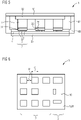
- FIG 6 a top view of another exemplary embodiment of the chip package 1 is shown.
- the plurality of semiconductor chips 2 arranged, for example, in a regular grid.
- the semiconductor chips 2 can be different types of the semiconductor chips 2, like IGBTs and diodes, having different thicknesses.
- the semiconductor chips 2 may have an edge length L.
- the edge length L is at least 0.2 mm and/or at most 2 mm or at most 2 cm.
- a distance D between adjacent semiconductor chips 2 may be smaller than the edge length L.
- said distance D may amount to at least 10% or at least 25% and/or to at most 100% or to at most 80% or to at most 65% of the edge length L.
- chip package described here is not restricted by the description on the basis of the exemplary embodiments. Rather, the chip package encompasses any new feature and also any combination of features, which includes in particular any combination of features in the patent claims, even if this feature or this combination itself is not explicitly specified in the patent claims or exemplary embodiments.
Landscapes
- Cooling Or The Like Of Semiconductors Or Solid State Devices (AREA)
- Printing Elements For Providing Electric Connections Between Printed Circuits (AREA)
- Die Bonding (AREA)
Priority Applications (4)
| Application Number | Priority Date | Filing Date | Title |
|---|---|---|---|
| EP21163949.7A EP4064345A1 (fr) | 2021-03-22 | 2021-03-22 | Boîtier de puce avec couche poreuse déformable élastiquement |
| CN202280024038.5A CN117121200A (zh) | 2021-03-22 | 2022-02-15 | 多孔的可弹性变形芯片封装 |
| JP2023558195A JP7734202B2 (ja) | 2021-03-22 | 2022-02-15 | チップパッケージ |
| PCT/EP2022/053689 WO2022199944A1 (fr) | 2021-03-22 | 2022-02-15 | Emballage de puce à couche poreuse élastiquement déformable |
Applications Claiming Priority (1)
| Application Number | Priority Date | Filing Date | Title |
|---|---|---|---|
| EP21163949.7A EP4064345A1 (fr) | 2021-03-22 | 2021-03-22 | Boîtier de puce avec couche poreuse déformable élastiquement |
Publications (1)
| Publication Number | Publication Date |
|---|---|
| EP4064345A1 true EP4064345A1 (fr) | 2022-09-28 |
Family
ID=75173014
Family Applications (1)
| Application Number | Title | Priority Date | Filing Date |
|---|---|---|---|
| EP21163949.7A Pending EP4064345A1 (fr) | 2021-03-22 | 2021-03-22 | Boîtier de puce avec couche poreuse déformable élastiquement |
Country Status (4)
| Country | Link |
|---|---|
| EP (1) | EP4064345A1 (fr) |
| JP (1) | JP7734202B2 (fr) |
| CN (1) | CN117121200A (fr) |
| WO (1) | WO2022199944A1 (fr) |
Citations (5)
| Publication number | Priority date | Publication date | Assignee | Title |
|---|---|---|---|---|
| US6320268B1 (en) | 1999-01-27 | 2001-11-20 | Abb (Schweiz) Ag | Power semiconductor module |
| US20020005578A1 (en) * | 1998-01-22 | 2002-01-17 | Hironori Kodama | Press contact type semiconductor device and converter using same |
| JP2005209784A (ja) * | 2004-01-21 | 2005-08-04 | Hitachi Ltd | 圧接型半導体装置、及びこれを用いた変換器 |
| US20140110827A1 (en) * | 2012-01-11 | 2014-04-24 | Panasonic Corporation | Pressed-contact type semiconductor device and method for manufacturing the same |
| JP2014127536A (ja) * | 2012-12-26 | 2014-07-07 | Hitachi Power Semiconductor Device Ltd | 複数の半導体素子を有する半導体装置 |
Family Cites Families (5)
| Publication number | Priority date | Publication date | Assignee | Title |
|---|---|---|---|---|
| JPH1187610A (ja) * | 1997-09-05 | 1999-03-30 | Mitsubishi Electric Corp | 半導体装置 |
| JP3617306B2 (ja) * | 1998-04-15 | 2005-02-02 | 株式会社日立製作所 | 加圧接触型半導体装置、及びこれを用いた変換器 |
| JP6216709B2 (ja) * | 2012-03-05 | 2017-10-18 | ナミックス株式会社 | 銀微粒子焼結体 |
| JP2015141952A (ja) * | 2014-01-27 | 2015-08-03 | 日本特殊陶業株式会社 | 半導体パワーモジュール |
| JP2020009989A (ja) * | 2018-07-12 | 2020-01-16 | 株式会社ジェイテクト | 半導体装置 |
-
2021
- 2021-03-22 EP EP21163949.7A patent/EP4064345A1/fr active Pending
-
2022
- 2022-02-15 CN CN202280024038.5A patent/CN117121200A/zh active Pending
- 2022-02-15 JP JP2023558195A patent/JP7734202B2/ja active Active
- 2022-02-15 WO PCT/EP2022/053689 patent/WO2022199944A1/fr not_active Ceased
Patent Citations (5)
| Publication number | Priority date | Publication date | Assignee | Title |
|---|---|---|---|---|
| US20020005578A1 (en) * | 1998-01-22 | 2002-01-17 | Hironori Kodama | Press contact type semiconductor device and converter using same |
| US6320268B1 (en) | 1999-01-27 | 2001-11-20 | Abb (Schweiz) Ag | Power semiconductor module |
| JP2005209784A (ja) * | 2004-01-21 | 2005-08-04 | Hitachi Ltd | 圧接型半導体装置、及びこれを用いた変換器 |
| US20140110827A1 (en) * | 2012-01-11 | 2014-04-24 | Panasonic Corporation | Pressed-contact type semiconductor device and method for manufacturing the same |
| JP2014127536A (ja) * | 2012-12-26 | 2014-07-07 | Hitachi Power Semiconductor Device Ltd | 複数の半導体素子を有する半導体装置 |
Also Published As
| Publication number | Publication date |
|---|---|
| JP2024516506A (ja) | 2024-04-16 |
| WO2022199944A1 (fr) | 2022-09-29 |
| JP7734202B2 (ja) | 2025-09-04 |
| CN117121200A (zh) | 2023-11-24 |
Similar Documents
| Publication | Publication Date | Title |
|---|---|---|
| US8520386B2 (en) | Power converter module with a cooled busbar arrangement | |
| CN107636827B (zh) | 功率电子设备模块 | |
| JP2003197864A (ja) | パワー半導体モジュール | |
| US6181007B1 (en) | Semiconductor device | |
| CN104465557A (zh) | 电子功率器件和制作电子功率器件的方法 | |
| US20180033711A1 (en) | Double-Encapsulated Power Semiconductor Module and Method for Producing the Same | |
| CN101673730A (zh) | 包括半导体器件的堆叠组件 | |
| US11888407B2 (en) | Power module having at least two power semiconductor arrangements that are contacted on a substrate | |
| JP3617306B2 (ja) | 加圧接触型半導体装置、及びこれを用いた変換器 | |
| CN116266576A (zh) | 功率半导体模块 | |
| US20200294883A1 (en) | Self-healing pdms encapsulation and repair of power modules | |
| KR20230159286A (ko) | 압축성 접착제를 사용한 반도체 디바이스 배열 | |
| JP2003197861A (ja) | 電力用半導体サブモジュール及び電力用半導体モジュール | |
| US20020154482A1 (en) | Press - contact type semiconductor device | |
| US20020060371A1 (en) | High-power semiconductor module, and use of such a high-power semiconductor module | |
| WO2022199944A1 (fr) | Emballage de puce à couche poreuse élastiquement déformable | |
| EP4227995B1 (fr) | Module d'électronique de puissance et son procédé de fabrication | |
| EP3513432B1 (fr) | Module de puissance type paquet pressé | |
| CN219350206U (zh) | 功率半导体模块 | |
| WO2021165483A1 (fr) | Module semi-conducteur de puissance | |
| JPH10290000A (ja) | 圧接型半導体装置 | |
| US20260090385A1 (en) | Semiconductor module comprising a housing | |
| WO2024245516A1 (fr) | Module de puissance à semiconducteur, boîtier de puissance à semiconducteur et procédé de fabrication d'un module de puissance à semiconducteur | |
| JPH11274185A (ja) | 圧接型半導体装置、及びこれを用いた変換器 | |
| US10103085B2 (en) | Clamping assembly having a pressure element |
Legal Events
| Date | Code | Title | Description |
|---|---|---|---|
| PUAI | Public reference made under article 153(3) epc to a published international application that has entered the european phase |
Free format text: ORIGINAL CODE: 0009012 |
|
| STAA | Information on the status of an ep patent application or granted ep patent |
Free format text: STATUS: THE APPLICATION HAS BEEN PUBLISHED |
|
| AK | Designated contracting states |
Kind code of ref document: A1 Designated state(s): AL AT BE BG CH CY CZ DE DK EE ES FI FR GB GR HR HU IE IS IT LI LT LU LV MC MK MT NL NO PL PT RO RS SE SI SK SM TR |
|
| STAA | Information on the status of an ep patent application or granted ep patent |
Free format text: STATUS: REQUEST FOR EXAMINATION WAS MADE |
|
| 17P | Request for examination filed |
Effective date: 20221129 |
|
| RBV | Designated contracting states (corrected) |
Designated state(s): AL AT BE BG CH CY CZ DE DK EE ES FI FR GB GR HR HU IE IS IT LI LT LU LV MC MK MT NL NO PL PT RO RS SE SI SK SM TR |
|
| P01 | Opt-out of the competence of the unified patent court (upc) registered |
Effective date: 20230527 |
|
| RAP1 | Party data changed (applicant data changed or rights of an application transferred) |
Owner name: HITACHI ENERGY LTD |
|
| STAA | Information on the status of an ep patent application or granted ep patent |
Free format text: STATUS: EXAMINATION IS IN PROGRESS |
|
| 17Q | First examination report despatched |
Effective date: 20240910 |