EP4074860B1 - Procédé de production d'une couche contenant du cuivre - Google Patents
Procédé de production d'une couche contenant du cuivre Download PDFInfo
- Publication number
- EP4074860B1 EP4074860B1 EP20899821.1A EP20899821A EP4074860B1 EP 4074860 B1 EP4074860 B1 EP 4074860B1 EP 20899821 A EP20899821 A EP 20899821A EP 4074860 B1 EP4074860 B1 EP 4074860B1
- Authority
- EP
- European Patent Office
- Prior art keywords
- copper
- substrate
- raw material
- containing layer
- thin
- Prior art date
- Legal status (The legal status is an assumption and is not a legal conclusion. Google has not performed a legal analysis and makes no representation as to the accuracy of the status listed.)
- Active
Links
Images

Classifications
-
- C—CHEMISTRY; METALLURGY
- C23—COATING METALLIC MATERIAL; COATING MATERIAL WITH METALLIC MATERIAL; CHEMICAL SURFACE TREATMENT; DIFFUSION TREATMENT OF METALLIC MATERIAL; COATING BY VACUUM EVAPORATION, BY SPUTTERING, BY ION IMPLANTATION OR BY CHEMICAL VAPOUR DEPOSITION, IN GENERAL; INHIBITING CORROSION OF METALLIC MATERIAL OR INCRUSTATION IN GENERAL
- C23C—COATING METALLIC MATERIAL; COATING MATERIAL WITH METALLIC MATERIAL; SURFACE TREATMENT OF METALLIC MATERIAL BY DIFFUSION INTO THE SURFACE, BY CHEMICAL CONVERSION OR SUBSTITUTION; COATING BY VACUUM EVAPORATION, BY SPUTTERING, BY ION IMPLANTATION OR BY CHEMICAL VAPOUR DEPOSITION, IN GENERAL
- C23C30/00—Coating with metallic material characterised only by the composition of the metallic material, i.e. not characterised by the coating process
-
- C—CHEMISTRY; METALLURGY
- C07—ORGANIC CHEMISTRY
- C07F—ACYCLIC, CARBOCYCLIC OR HETEROCYCLIC COMPOUNDS CONTAINING ELEMENTS OTHER THAN CARBON, HYDROGEN, HALOGEN, OXYGEN, NITROGEN, SULFUR, SELENIUM OR TELLURIUM
- C07F1/00—Compounds containing elements of Groups 1 or 11 of the Periodic Table
- C07F1/08—Copper compounds
-
- C—CHEMISTRY; METALLURGY
- C09—DYES; PAINTS; POLISHES; NATURAL RESINS; ADHESIVES; COMPOSITIONS NOT OTHERWISE PROVIDED FOR; APPLICATIONS OF MATERIALS NOT OTHERWISE PROVIDED FOR
- C09D—COATING COMPOSITIONS, e.g. PAINTS, VARNISHES OR LACQUERS; FILLING PASTES; CHEMICAL PAINT OR INK REMOVERS; INKS; CORRECTING FLUIDS; WOODSTAINS; PASTES OR SOLIDS FOR COLOURING OR PRINTING; USE OF MATERIALS THEREFOR
- C09D1/00—Coating compositions, e.g. paints, varnishes or lacquers, based on inorganic substances
-
- C—CHEMISTRY; METALLURGY
- C23—COATING METALLIC MATERIAL; COATING MATERIAL WITH METALLIC MATERIAL; CHEMICAL SURFACE TREATMENT; DIFFUSION TREATMENT OF METALLIC MATERIAL; COATING BY VACUUM EVAPORATION, BY SPUTTERING, BY ION IMPLANTATION OR BY CHEMICAL VAPOUR DEPOSITION, IN GENERAL; INHIBITING CORROSION OF METALLIC MATERIAL OR INCRUSTATION IN GENERAL
- C23C—COATING METALLIC MATERIAL; COATING MATERIAL WITH METALLIC MATERIAL; SURFACE TREATMENT OF METALLIC MATERIAL BY DIFFUSION INTO THE SURFACE, BY CHEMICAL CONVERSION OR SUBSTITUTION; COATING BY VACUUM EVAPORATION, BY SPUTTERING, BY ION IMPLANTATION OR BY CHEMICAL VAPOUR DEPOSITION, IN GENERAL
- C23C16/00—Chemical coating by decomposition of gaseous compounds, without leaving reaction products of surface material in the coating, i.e. chemical vapour deposition [CVD] processes
- C23C16/02—Pretreatment of the material to be coated
-
- C—CHEMISTRY; METALLURGY
- C23—COATING METALLIC MATERIAL; COATING MATERIAL WITH METALLIC MATERIAL; CHEMICAL SURFACE TREATMENT; DIFFUSION TREATMENT OF METALLIC MATERIAL; COATING BY VACUUM EVAPORATION, BY SPUTTERING, BY ION IMPLANTATION OR BY CHEMICAL VAPOUR DEPOSITION, IN GENERAL; INHIBITING CORROSION OF METALLIC MATERIAL OR INCRUSTATION IN GENERAL
- C23C—COATING METALLIC MATERIAL; COATING MATERIAL WITH METALLIC MATERIAL; SURFACE TREATMENT OF METALLIC MATERIAL BY DIFFUSION INTO THE SURFACE, BY CHEMICAL CONVERSION OR SUBSTITUTION; COATING BY VACUUM EVAPORATION, BY SPUTTERING, BY ION IMPLANTATION OR BY CHEMICAL VAPOUR DEPOSITION, IN GENERAL
- C23C16/00—Chemical coating by decomposition of gaseous compounds, without leaving reaction products of surface material in the coating, i.e. chemical vapour deposition [CVD] processes
- C23C16/02—Pretreatment of the material to be coated
- C23C16/0209—Pretreatment of the material to be coated by heating
- C23C16/0218—Pretreatment of the material to be coated by heating in a reactive atmosphere
-
- C—CHEMISTRY; METALLURGY
- C23—COATING METALLIC MATERIAL; COATING MATERIAL WITH METALLIC MATERIAL; CHEMICAL SURFACE TREATMENT; DIFFUSION TREATMENT OF METALLIC MATERIAL; COATING BY VACUUM EVAPORATION, BY SPUTTERING, BY ION IMPLANTATION OR BY CHEMICAL VAPOUR DEPOSITION, IN GENERAL; INHIBITING CORROSION OF METALLIC MATERIAL OR INCRUSTATION IN GENERAL
- C23C—COATING METALLIC MATERIAL; COATING MATERIAL WITH METALLIC MATERIAL; SURFACE TREATMENT OF METALLIC MATERIAL BY DIFFUSION INTO THE SURFACE, BY CHEMICAL CONVERSION OR SUBSTITUTION; COATING BY VACUUM EVAPORATION, BY SPUTTERING, BY ION IMPLANTATION OR BY CHEMICAL VAPOUR DEPOSITION, IN GENERAL
- C23C16/00—Chemical coating by decomposition of gaseous compounds, without leaving reaction products of surface material in the coating, i.e. chemical vapour deposition [CVD] processes
- C23C16/02—Pretreatment of the material to be coated
- C23C16/0227—Pretreatment of the material to be coated by cleaning or etching
- C23C16/0245—Pretreatment of the material to be coated by cleaning or etching by etching with a plasma
-
- C—CHEMISTRY; METALLURGY
- C23—COATING METALLIC MATERIAL; COATING MATERIAL WITH METALLIC MATERIAL; CHEMICAL SURFACE TREATMENT; DIFFUSION TREATMENT OF METALLIC MATERIAL; COATING BY VACUUM EVAPORATION, BY SPUTTERING, BY ION IMPLANTATION OR BY CHEMICAL VAPOUR DEPOSITION, IN GENERAL; INHIBITING CORROSION OF METALLIC MATERIAL OR INCRUSTATION IN GENERAL
- C23C—COATING METALLIC MATERIAL; COATING MATERIAL WITH METALLIC MATERIAL; SURFACE TREATMENT OF METALLIC MATERIAL BY DIFFUSION INTO THE SURFACE, BY CHEMICAL CONVERSION OR SUBSTITUTION; COATING BY VACUUM EVAPORATION, BY SPUTTERING, BY ION IMPLANTATION OR BY CHEMICAL VAPOUR DEPOSITION, IN GENERAL
- C23C16/00—Chemical coating by decomposition of gaseous compounds, without leaving reaction products of surface material in the coating, i.e. chemical vapour deposition [CVD] processes
- C23C16/06—Chemical coating by decomposition of gaseous compounds, without leaving reaction products of surface material in the coating, i.e. chemical vapour deposition [CVD] processes characterised by the deposition of metallic material
- C23C16/18—Chemical coating by decomposition of gaseous compounds, without leaving reaction products of surface material in the coating, i.e. chemical vapour deposition [CVD] processes characterised by the deposition of metallic material from metallo-organic compounds
-
- C—CHEMISTRY; METALLURGY
- C23—COATING METALLIC MATERIAL; COATING MATERIAL WITH METALLIC MATERIAL; CHEMICAL SURFACE TREATMENT; DIFFUSION TREATMENT OF METALLIC MATERIAL; COATING BY VACUUM EVAPORATION, BY SPUTTERING, BY ION IMPLANTATION OR BY CHEMICAL VAPOUR DEPOSITION, IN GENERAL; INHIBITING CORROSION OF METALLIC MATERIAL OR INCRUSTATION IN GENERAL
- C23C—COATING METALLIC MATERIAL; COATING MATERIAL WITH METALLIC MATERIAL; SURFACE TREATMENT OF METALLIC MATERIAL BY DIFFUSION INTO THE SURFACE, BY CHEMICAL CONVERSION OR SUBSTITUTION; COATING BY VACUUM EVAPORATION, BY SPUTTERING, BY ION IMPLANTATION OR BY CHEMICAL VAPOUR DEPOSITION, IN GENERAL
- C23C16/00—Chemical coating by decomposition of gaseous compounds, without leaving reaction products of surface material in the coating, i.e. chemical vapour deposition [CVD] processes
- C23C16/44—Chemical coating by decomposition of gaseous compounds, without leaving reaction products of surface material in the coating, i.e. chemical vapour deposition [CVD] processes characterised by the method of coating
- C23C16/455—Chemical coating by decomposition of gaseous compounds, without leaving reaction products of surface material in the coating, i.e. chemical vapour deposition [CVD] processes characterised by the method of coating characterised by the method used for introducing gases into reaction chamber or for modifying gas flows in reaction chamber
- C23C16/45523—Pulsed gas flow or change of composition over time
- C23C16/45525—Atomic layer deposition [ALD]
- C23C16/45527—Atomic layer deposition [ALD] characterized by the ALD cycle, e.g. different flows or temperatures during half-reactions, unusual pulsing sequence, use of precursor mixtures or auxiliary reactants or activations
- C23C16/45536—Use of plasma, radiation or electromagnetic fields
-
- C—CHEMISTRY; METALLURGY
- C23—COATING METALLIC MATERIAL; COATING MATERIAL WITH METALLIC MATERIAL; CHEMICAL SURFACE TREATMENT; DIFFUSION TREATMENT OF METALLIC MATERIAL; COATING BY VACUUM EVAPORATION, BY SPUTTERING, BY ION IMPLANTATION OR BY CHEMICAL VAPOUR DEPOSITION, IN GENERAL; INHIBITING CORROSION OF METALLIC MATERIAL OR INCRUSTATION IN GENERAL
- C23C—COATING METALLIC MATERIAL; COATING MATERIAL WITH METALLIC MATERIAL; SURFACE TREATMENT OF METALLIC MATERIAL BY DIFFUSION INTO THE SURFACE, BY CHEMICAL CONVERSION OR SUBSTITUTION; COATING BY VACUUM EVAPORATION, BY SPUTTERING, BY ION IMPLANTATION OR BY CHEMICAL VAPOUR DEPOSITION, IN GENERAL
- C23C16/00—Chemical coating by decomposition of gaseous compounds, without leaving reaction products of surface material in the coating, i.e. chemical vapour deposition [CVD] processes
- C23C16/44—Chemical coating by decomposition of gaseous compounds, without leaving reaction products of surface material in the coating, i.e. chemical vapour deposition [CVD] processes characterised by the method of coating
- C23C16/455—Chemical coating by decomposition of gaseous compounds, without leaving reaction products of surface material in the coating, i.e. chemical vapour deposition [CVD] processes characterised by the method of coating characterised by the method used for introducing gases into reaction chamber or for modifying gas flows in reaction chamber
- C23C16/45523—Pulsed gas flow or change of composition over time
- C23C16/45525—Atomic layer deposition [ALD]
- C23C16/45527—Atomic layer deposition [ALD] characterized by the ALD cycle, e.g. different flows or temperatures during half-reactions, unusual pulsing sequence, use of precursor mixtures or auxiliary reactants or activations
- C23C16/45536—Use of plasma, radiation or electromagnetic fields
- C23C16/45542—Plasma being used non-continuously during the ALD reactions
-
- C—CHEMISTRY; METALLURGY
- C23—COATING METALLIC MATERIAL; COATING MATERIAL WITH METALLIC MATERIAL; CHEMICAL SURFACE TREATMENT; DIFFUSION TREATMENT OF METALLIC MATERIAL; COATING BY VACUUM EVAPORATION, BY SPUTTERING, BY ION IMPLANTATION OR BY CHEMICAL VAPOUR DEPOSITION, IN GENERAL; INHIBITING CORROSION OF METALLIC MATERIAL OR INCRUSTATION IN GENERAL
- C23C—COATING METALLIC MATERIAL; COATING MATERIAL WITH METALLIC MATERIAL; SURFACE TREATMENT OF METALLIC MATERIAL BY DIFFUSION INTO THE SURFACE, BY CHEMICAL CONVERSION OR SUBSTITUTION; COATING BY VACUUM EVAPORATION, BY SPUTTERING, BY ION IMPLANTATION OR BY CHEMICAL VAPOUR DEPOSITION, IN GENERAL
- C23C16/00—Chemical coating by decomposition of gaseous compounds, without leaving reaction products of surface material in the coating, i.e. chemical vapour deposition [CVD] processes
- C23C16/44—Chemical coating by decomposition of gaseous compounds, without leaving reaction products of surface material in the coating, i.e. chemical vapour deposition [CVD] processes characterised by the method of coating
- C23C16/455—Chemical coating by decomposition of gaseous compounds, without leaving reaction products of surface material in the coating, i.e. chemical vapour deposition [CVD] processes characterised by the method of coating characterised by the method used for introducing gases into reaction chamber or for modifying gas flows in reaction chamber
- C23C16/45523—Pulsed gas flow or change of composition over time
- C23C16/45525—Atomic layer deposition [ALD]
- C23C16/45553—Atomic layer deposition [ALD] characterized by the use of precursors specially adapted for ALD
-
- H—ELECTRICITY
- H10—SEMICONDUCTOR DEVICES; ELECTRIC SOLID-STATE DEVICES NOT OTHERWISE PROVIDED FOR
- H10P—GENERIC PROCESSES OR APPARATUS FOR THE MANUFACTURE OR TREATMENT OF DEVICES COVERED BY CLASS H10
- H10P14/00—Formation of materials, e.g. in the shape of layers or pillars
- H10P14/40—Formation of materials, e.g. in the shape of layers or pillars of conductive or resistive materials
- H10P14/42—Formation of materials, e.g. in the shape of layers or pillars of conductive or resistive materials using a gas or vapour
- H10P14/43—Chemical deposition, e.g. chemical vapour deposition [CVD]
- H10P14/432—Chemical deposition, e.g. chemical vapour deposition [CVD] using selective deposition
-
- H—ELECTRICITY
- H10—SEMICONDUCTOR DEVICES; ELECTRIC SOLID-STATE DEVICES NOT OTHERWISE PROVIDED FOR
- H10W—GENERIC PACKAGES, INTERCONNECTIONS, CONNECTORS OR OTHER CONSTRUCTIONAL DETAILS OF DEVICES COVERED BY CLASS H10
- H10W20/00—Interconnections in chips, wafers or substrates
- H10W20/01—Manufacture or treatment
- H10W20/031—Manufacture or treatment of conductive parts of the interconnections
- H10W20/032—Manufacture or treatment of conductive parts of the interconnections of conductive barrier, adhesion or liner layers
- H10W20/052—Manufacture or treatment of conductive parts of the interconnections of conductive barrier, adhesion or liner layers by treatments not introducing additional elements therein
- H10W20/0523—Manufacture or treatment of conductive parts of the interconnections of conductive barrier, adhesion or liner layers by treatments not introducing additional elements therein by irradiating with ultraviolet or particle radiation
Definitions
- the present invention relates to a method of producing a copper-containing layer having a low electrical resistivity.
- the number of elements per unit area is increased and a distance between elements is shortened by narrowing a wiring width and a wiring distance of a metal wiring circuit, and thus a drive voltage can be reduced.
- the semiconductor thus highly integrated can achieve a high-speed operation and a low-power consumption operation.
- an electronic device can achieve downsizing/weight saving and improvements in function and performance, and reductions in power consumption and cost.
- the wiring width is narrowed, there is a high risk in that electromigration occurs owing to increases in resistance per unit length and current density, resulting in a failure of the semiconductor. Accordingly, a semiconductor using copper, which is less liable to be affected by the electromigration, as a conductive material has increasingly been manufactured.
- Patent Document 1 As the semiconductor using copper as a conductive material, for example, in Patent Document 1, there is a proposal of a product in which a tantalum layer is formed by a physical vapor deposition (PVD) method on a tantalum nitride layer formed by an atomic layer deposition (ALD) method, and further, copper is formed by the PVD method on the tantalum layer.
- PVD physical vapor deposition
- ALD atomic layer deposition
- Non Patent Document 1 there is a description that a metal film of copper, which is formed on a substrate formed of silica, titanium nitride, tantalum, or the like through use of a copper complex by a plasma ALD method, has a low electrical resistivity. Further relevant prior art is disclosed in patent document 2 and patent document 3, as well as in non patent document 2.
- a method of producing a copper-containing layer including: step 1: a step of reducing a surface of a substrate, provided that a substrate having a surface formed of a silicic acid compound is excluded, through use of a reducing agent;
- a thickness of the copper containing layer is 20 nm or less.
- a copper-containing layer having a low electrical resistivity can be produced.
- production method of the present invention A method of producing a copper-containing layer of the present invention (hereinafter referred to as "production method of the present invention") is described.
- the production method of the present invention is characterized by including: a step 1 of reducing a substrate through use of a reducing agent; and a step 2 of, after the step 1, forming a copper-containing layer on the substrate through use of a thin-film forming raw material containing a copper compound by a plasma ALD method.
- a well-known plasma ALD apparatus enabling plasma treatment of a reactive gas may be used in the production method of the present invention.
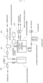
- Specific examples of the plasma ALD apparatus include: an apparatus as illustrated in FIG.
- the apparatus is not limited to a single-substrate type apparatus including a film formation chamber as illustrated in each of FIG. 1 and FIG. 2 , and an apparatus capable of simultaneously processing a large number of substrates through use of a batch furnace may also be used.
- step 1 of the production method of the present invention is described.
- the step 1 is a process of subjecting the surface of the substrate to reduction treatment by bringing the reducing agent into contact with the surface of the substrate while applying heat to the substrate as required. It is preferred that the step 1 be performed by the plasma ALD apparatus, and it is preferred that the step 1 and the step 2 be continuously performed by the plasma ALD apparatus.
- the substrate used in the production method of the present invention is a substrate except a substrate having a surface formed of a silicic acid compound, and is a metal substrate or a substrate having a metal film formed on a surface thereof, for example, a metal selected from the group consisting of: aluminum; silver; gold; lead; vanadium; manganese; magnesium; iron; cobalt; nickel; copper; chromium; palladium; molybdenum; tungsten; platinum; titanium; zirconium; and zinc, and an alloy, such as brass, bronze, steel, stainless steel, an aluminum alloy, a magnesium alloy, or a titanium alloy.
- a metal selected from the group consisting of: aluminum; silver; gold; lead; vanadium; manganese; magnesium; iron; cobalt; nickel; copper; chromium; palladium; molybdenum; tungsten; platinum; titanium; zirconium; and zinc, and an alloy, such as brass, bronze, steel, stainless steel, an aluminum alloy, a magnesium alloy,
- a substrate having a surface formed of a silicic acid compound is excluded because the effect of the present invention cannot be obtained, a substrate having a metal film formed on the surface of the silicic acid compound is used in the production method of the present invention.
- a formation method for the metal film there is given a method involving forming the metal film on the surface of the substrate through use of a metal compound by an ALD method or a CVD method.
- An example of the metal compound is "the other precursor" to be described later.
- the shape of the substrate is, for example, a plate shape, a spherical shape, a fibrous shape, or a scaly shape.
- the surface of the substrate may be planar, or may have a three-dimensional structure, such as a trench structure.
- a metal is reduced by bringing the reducing agent (gas) into contact with the surface of the substrate.
- the substrate may be heated, or heat may be applied thereto by heating the film formation chamber.
- the step 1 is preferably performed at a temperature within the range of from 20°C to 400°C. When the temperature is less than 20°C, there is no apparatus that can be handled at the temperature. Meanwhile, when the temperature is more than 400°C, the substrate cannot withstand damage due to heat in some cases.
- the reducing agent includes hydrogen, carbon monoxide, hydrogen sulfide, sulfur dioxide, ammonia, hydrazine, monosilane, disilane, diborane, trimethylaluminum (TMA), and diethylzinc (ZnEt 2 ), and products obtained by subjecting those reducing agents to plasma treatment may also be used.
- at least one selected from the group consisting of: hydrogen; ammonia; hydrazine; monosilane; disilane; diborane; trimethylaluminum; diethylzinc; and plasma thereof is used as the reducing agent.
- hydrogen plasma is more preferably used from the viewpoints of causing less damage to the substrate and less influence on film contamination, and enabling a reduction in film formation temperature.
- introduction method for the reducing agent into the film formation chamber for example, decompression of the film formation chamber may be adopted.
- a plasma treatment method for the reducing agent there is given, for example, a method involving radiating plasma emitted from a coil electrode to the reducing agent.
- the plasma include: capacitively coupled plasma generated by an electrostatic field caused by a high-frequency voltage applied to the coil electrode; and inductively coupled plasma by an induction field generated by a high-frequency current flowing through the coil electrode.
- Those plasmas can each be generated in a separate location from the substrate, and hence damage caused by the plasma to the substrate can be suppressed.
- a plasma excitation frequency during the radiation of the plasma to the reducing agent is preferably 13.56 MHz, and a plasma output is preferably from 1 W to 600 W, more preferably from 20 W to 200 W.
- a plasma output is preferably from 1 W to 600 W, more preferably from 20 W to 200 W.
- the output is less than 20 W, the effect of the present invention may not be obtained. Meanwhile, when the output is more than 200 W, damage to the substrate may be increased.
- the reducing agent (gas) is preferably evacuated from the film formation chamber.
- the reducing agent (gas) be completely evacuated from the film formation chamber, but it is not always required that the reducing agent (gas) be completely evacuated.
- an evacuation method there are given, for example, a method involving purging the inside of the film formation chamber with an inert gas, such as helium, nitrogen, or argon, a method involving performing evacuation by decompressing the inside of the film formation chamber, and a combination of these methods.
- the degree of decompression in the case of performing decompression falls within the range of preferably from 0.01 Pa to 300 Pa, more preferably from 0.01 Pa to 100 Pa.
- the step 2 is a process of forming the copper-containing layer on the surface having been reduced in the step 1 through use of the thin-film forming raw material containing a copper compound by the plasma ALD method.
- the step 2 includes: a step (raw material gas introduction step) of introducing vapor obtained by vaporizing the thin-film forming raw material containing a copper compound and vapor of another precursor to be used as required (hereinafter referred to as "raw material gas”) into the film formation chamber; a step (precursor layer formation step) of depositing the copper compound in the raw material gas on the surface of the substrate, to thereby form a precursor layer; a step (evacuation step) of evacuating the raw material gas remaining unreacted; and a step (copper-containing layer formation step) of introducing plasma of a reactive gas into the film formation chamber to cause the precursor layer and the plasma of the reactive gas to react with each other, to thereby form a copper-containing layer on the surface of the substrate.
- a step of vaporizing the thin-film forming raw material to obtain vapor (raw material gas) may be performed in a raw material container, or may be performed in a vaporization chamber after the thin-film forming raw material is introduced into the vaporization chamber.
- the raw material gas introduction step as a transportation and supply method at the time of introducing the raw material gas into the film formation chamber, there are specifically given, for example: a gas transportation method involving heating and/or decompressing the thin-film forming raw material in a storage container (hereinafter referred to as “raw material container”), to thereby vaporize the raw material to obtain a raw material gas, and introducing the raw material gas into the film formation chamber (hereinafter referred to as "deposition reaction portion") having the substrate set therein together with a carrier gas, such as argon, nitrogen, or helium, as required as illustrated in FIG.
- a carrier gas such as argon, nitrogen, or helium
- the copper compound itself may be used as the thin-film forming raw material.
- the copper compound itself or a solution obtained by dissolving the copper compound in an organic solvent may be used as the thin-film forming raw material.
- the thin-film forming raw material may further contain a nucleophilic reagent or the like.
- the thin-film forming raw material is preferably vaporized at 20°C to 200°C.
- the pressure in the raw material container and the pressure in the vaporization chamber preferably fall within the range of from 1 Pa to 10,000 Pa.
- the copper compound contained in the thin-film forming raw material only needs to be capable of forming a thin-film of copper, and the structure of the copper compound is not particularly limited. However, when the copper compound has a molecular weight of more than 1,000, its melting point becomes too high, with the result that its utilization as the thin-film forming raw material may be difficult.
- the copper compound has a molecular weight of preferably less than 800, more preferably from 200 to 600.
- the copper compound has a melting point of preferably 50°C or less, and is more preferably a liquid at normal temperature in order to ensure, in an apparatus for producing a thin-film through use of the thin-film forming raw material, transportability in piping of the apparatus.
- “Me” represents a “methyl group”
- “Et” represents an “ethyl group”
- “iPr” represents an “isopropyl group”
- "nPr” represents a “n-propyl group”
- "tBu” represents a “tert-butyl group”
- sBu represents a "sec-butyl group
- nBu represents a "n-butyl group”
- SiMe 3 represents a "trimethylsilyl group”.
- a copper compound represented by the following general formula (1) is used in the production method of the present invention because the compound has a high vapor pressure and is excellent in thermal stability.
- R 1 , R 2 , R 5 , and R 6 each independently represent a hydrogen atom, an alkyl group having 1 to 4 carbon atoms, or a halogen atom
- R 3 , R 4 , R 7 , and R 8 each independently represent an alkyl group having 1 to 4 carbon atoms or a halogen atom.
- the alkyl group having 1 to 4 carbon atoms represented by each of R 1 to R 8 in the above-mentioned general formula (1) may be linear or branched.
- Specific examples of the alkyl group having 1 to 4 carbon atoms include a methyl group, an ethyl group, a propyl group, an isopropyl group, a n-butyl group, a sec-butyl group, a tert-butyl group, and an isobutyl group.
- An alkyl group having more than 4 carbon atoms causes an increase in melting point, which may make the thin-film forming raw material unusable.
- the alkyl group preferably has 1 to 3 carbon atoms.
- a copper compound in which R 1 and R 5 each represent a methyl group, and R 2 and R 6 each represent a hydrogen atom is preferred, and a copper compound in which R 1 and R 5 each represent a methyl group, R 2 and R 6 each represent a hydrogen atom, and R 3 , R 4 , R 7 , and R 8 each represent a group selected from the group consisting of: a methyl group; an ethyl group; and an isopropyl group is more preferred.
- Examples of the halogen atom represented by each of R 1 to R 8 in the above-mentioned general formula (1) include a fluorine atom, a chlorine atom, a bromine atom, and an iodine atom. Of those, a chlorine atom is preferred.
- the copper compound represented by the above-mentioned general formula (1) include the compound 5 to the compound 16 described above, but the production method of the present invention is not limited by these copper compounds.
- a production method for the above-mentioned copper compound is not particularly limited, and the copper compound is produced through application of a well-known reaction.
- the copper compound may be obtained by a production method described in JP 2015-218117 A .
- the thin-film forming raw material only needs to contain the copper compound and be usable as a precursor of a thin-film, and the composition thereof varies depending on the kind of a target thin-film.
- the thin-film forming raw material when a thin-film containing only copper as a metal is to be produced, the thin-film forming raw material is free of a metal compound other than copper and a semimetal compound.
- the thin-film forming raw material may contain a compound containing a desired metal and/or a compound containing a semimetal (hereinafter referred to as "other precursor") in addition to the copper compound.
- a multi-component ALD method in which a plurality of precursors are used, there is no particular limitation on the other precursor that may be used together with the copper compound, and a well-known general precursor used for the thin-film forming raw material for an ALD method may be used.
- Examples of the above-mentioned other precursor include compounds each formed of: one kind or two or more kinds selected from the group consisting of compounds used as organic ligands, such as an alcohol compound, a glycol compound, a ⁇ -diketone compound, a cyclopentadiene compound, and an organic amine compound; and a metal.
- compounds used as organic ligands such as an alcohol compound, a glycol compound, a ⁇ -diketone compound, a cyclopentadiene compound, and an organic amine compound.
- examples of the kind of the metal in the precursor include lithium, sodium, potassium, magnesium, calcium, strontium, barium, titanium, zirconium, hafnium, vanadium, niobium, tantalum, chromium, tungsten, manganese, iron, osmium, ruthenium, cobalt, rhodium, iridium, nickel, palladium, platinum, silver, gold, zinc, aluminum, gallium, indium, germanium, tin, lead, antimony, bismuth, radium, scandium, ruthenium, yttrium, lanthanum, cerium, praseodymium, neodymium, promethium, samarium, europium, gadolinium, terbium, dysprosium, holmium, erbium, thulium, ytterbium, and lutetium.
- Examples of the alcohol compound to be used as the organic ligand in the above-mentioned other precursor include: alkyl alcohols, such as methanol, ethanol, propanol, isopropyl alcohol, butanol, sec-butyl alcohol, isobutyl alcohol, tert-butyl alcohol, pentyl alcohol, isopentyl alcohol, and tert-pentyl alcohol; ether alcohols, such as 2-methoxyethanol, 2-ethoxyethanol, 2-butoxyethanol, 2-(2-methoxyethoxy)ethanol, 2-methoxy-1-methylethanol, 2-methoxy-1,1-dimethylethanol, 2-ethoxy-1,1-dimethylethanol, 2-isopropoxy-1,1-dimethylethanol, 2-butoxy-1,1-dimethylethanol, 2-(2-methoxyethoxy)-1,1-dimethylethanol, 2-propoxy-1,1-diethylethanol, 2-sec-butoxy-1,1-diethylethanol, and 3-methoxy
- glycol compound to be used as the organic ligand in the above-mentioned other precursor examples include 1,2-ethanediol, 1,2-propanediol, 1,3-propanediol, 2,4-hexanediol, 2,2-dimethyl-1,3-propanediol, 2,2-diethyl-1,3-propanediol, 1,3-butanediol, 2,4-butanediol, 2,2-diethyl-1,3-butanediol, 2-ethyl-2-butyl-1,3-propanediol, 2,4-pentanediol, 2-methyl-1,3-propanediol, 2-methyl-2,4-pentanediol, 2,4-hexanediol, and 2,4-dimethyl-2,4-pentanediol.
- Examples of the ⁇ -diketone compound to be used as the organic ligand in the above-mentioned other precursor include: alkyl-substituted ⁇ -diketones, such as acetylacetone, hexane-2,4-dione, 5-methylhexane-2,4-dione, heptane-2,4-dione, 2-methylheptane-3,5-dione, 5-methylheptane-2,4-dione, 6-methylheptane-2,4-dione, 2,2-dimethylheptane-3,5-dione, 2,6-dimethylheptane-3,5-dione, 2,2,6-trimethylheptane-3,5-dione, 2,2,6,6-tetramethylheptane-3,5-dione, octane-2,4-dione, 2,2,6-trimethyloctane-3,5-dione, 2,6-dimethyloc
- cyclopentadiene compound to be used as the organic ligand in the above-mentioned other precursor examples include cyclopentadiene, methylcyclopentadiene, ethylcyclopentadiene, propylcyclopentadiene, isopropylcyclopentadiene, butylcyclopentadiene, sec-butylcyclopentadiene, isobutylcyclopentadiene, tert-butylcyclopentadiene, dimethylcyclopentadiene, and tetramethylcyclopentadiene.
- Examples of the organic amine compound to be used as the above-mentioned organic ligand include methylamine, ethylamine, propylamine, isopropylamine, butylamine, sec-butylamine, tert-butylamine, isobutylamine, dimethylamine, diethylamine, dipropylamine, diisopropylamine, ethylmethylamine, propylmethylamine, and isopropylmethylamine.
- the precursor when the alcohol compound is used as the organic ligand, the precursor may be produced through a reaction between an inorganic salt of the metal described above or a hydrate thereof and an alkali metal alkoxide of the alcohol compound.
- examples of the inorganic salt of the metal or the hydrate thereof may include a halide and a nitrate of the metal
- examples of the alkali metal alkoxide may include a sodium alkoxide, a lithium alkoxide, and a potassium alkoxide.
- Examples of the multi-component ALD method as described above include: a method involving vaporizing and supplying each component of the thin-film forming raw material independently (hereinafter referred to as “single source method”); and a method involving vaporizing and supplying a mixed raw material obtained by mixing multi-component raw materials in accordance with desired composition in advance (hereinafter referred to as “cocktail source method”).
- the above-mentioned other precursor is preferably a compound similar to the copper compound in the behavior of thermal decomposition and/or oxidative decomposition.
- the above-mentioned other precursor is preferably a compound that not only is similar to the copper compound in the behavior of thermal decomposition and/or oxidative decomposition but also is prevented from being altered through a chemical reaction or the like at the time of mixing.
- a mixture of the copper compound and the other precursor, or a mixed solution obtained by dissolving the mixture in an organic solvent may be used as the thin-film forming raw material.
- organic solvent there is no particular limitation on the above-mentioned organic solvent, and a well-known general organic solvent may be used.
- organic solvent include: acetic acid esters, such as ethyl acetate, butyl acetate, and methoxyethyl acetate; ethers, such as tetrahydrofuran, tetrahydropyran, ethylene glycol dimethyl ether, diethylene glycol dimethyl ether, triethylene glycol dimethyl ether, dibutyl ether, and dioxane; ketones, such as methyl butyl ketone, methyl isobutyl ketone, ethyl butyl ketone, dipropyl ketone, diisobutyl ketone, methyl pentyl ketone, cyclohexanone, and methylcyclohexanone; hydrocarbons, such as hexane, cyclohexane, methylcyclohexane, dimethylcycl
- the thin-film forming raw material to be used in the production method of the present invention is the above-mentioned mixed solution
- the thin-film forming raw material is prepared so that the amount of the entire precursors in the thin-film forming raw material is preferably from 0.01 mol/liter to 2.0 mol/liter, more preferably from 0.05 mol/liter to 1.0 mol/liter.
- the amount of the entire precursors refers to the amount of the copper compound when the thin-film forming raw material is free of the metal compound other than the copper compound and the semimetal compound, and to the total amount of the copper compound and the other precursor when the thin-film forming raw material contains the other precursor.
- the thin-film forming raw material to be used in the production method of the present invention may contain a nucleophilic reagent as required in order to improve the stability of each of the copper compound and the other precursor.
- the nucleophilic reagent include: ethylene glycol ethers, such as glyme, diglyme, triglyme, and tetraglyme; crown ethers, such as 18-crown-6, dicyclohexyl-18-crown-6, 24-crown-8, dicyclohexyl-24-crown-8, and dibenzo-24-crown-8; polyamines, such as ethylenediamine, N,N'-tetramethylethylenediamine, diethylenetriamine, triethylenetetramine, tetraethylenepentamine, pentaethylenehexamine, 1,1,4,7,7-pentamethyldiethylenetriamine, 1,1,4,7,10,10-hexamethyltriethylenetetramine, and triethoxytriethylene
- the thin-film forming raw material be prevented from including impurity metal elements other than the components for forming the raw material, impurity halogens such as impurity chlorine, and impurity organic substances to the extent possible.
- the content of each of the impurity metal elements is preferably 100 ppb or less, more preferably 10 ppb or less, and the total content thereof is preferably 1 ppm or less, more preferably 100 ppb or less.
- the raw material when used as a gate insulating film, a gate film, or a barrier layer of an LSI, it is required to reduce the contents of alkali metal elements and alkaline-earth metal elements that influence the electrical characteristics of a thin-film to be obtained.
- the content of the impurity halogens is preferably 100 ppm or less, more preferably 10 ppm or less, still more preferably 1 ppm or less.
- the total content of the impurity organic substances is preferably 500 ppm or less, more preferably 50 ppm or less, still more preferably 10 ppm or less.
- moisture causes generation of particles in the thin-film forming raw material and during thin-film formation.
- the moisture is desirably removed as much as possible in advance at the time of use.
- the moisture content of each of the precursor, the organic solvent, and the nucleophilic reagent is preferably 10 ppm or less, more preferably 1 ppm or less.
- the thin-film forming raw material be prevented from including particles to the extent possible in order to reduce or prevent particle contamination of a thin-film to be formed.
- the number of particles larger than 0.3 ⁇ m be 100 or less in 1 ml of the liquid phase, and it is more preferred that the number of particles larger than 0.2 ⁇ m be 100 or less in 1 ml of the liquid phase.
- the raw material gas is introduced to the substrate set in the deposition reaction portion to deposit the copper compound in the raw material gas on the surface of the substrate, to thereby form the precursor layer on the substrate.
- the substrate may be heated, or heat may be applied thereto by heating the deposition reaction portion.
- a reaction temperature substrate temperature
- a reaction pressure reaction pressure
- a deposition rate and the like may appropriately be determined depending on the kind of the thin-film forming raw material.
- the reaction temperature is preferably not less than 20°C that is the temperature at which the thin-film forming raw material sufficiently reacts, more preferably from 20°C to 400°C, and the thin-film forming raw material is used within an ALD window adapted to the plasma of the reactive gas.
- the film thickness is controlled by the number of cycles so that a desired film thickness is obtained.
- the reaction pressure is preferably from 1 Pa to 10,000 Pa, more preferably from 10 Pa to 1,000 Pa.
- the other precursor is also deposited on the surface of the substrate together with the copper compound.
- the raw material gas not having been deposited on the surface of the substrate is evacuated from the deposition reaction portion. It is ideal that the raw material gas be completely evacuated from the deposition reaction portion, but it is not always required that the gas be completely evacuated.
- an evacuation method there are given, for example, a method involving purging the inside of the deposition reaction portion with an inert gas, such as helium, nitrogen, or argon, a method involving performing evacuation by decompressing the inside of the deposition reaction portion, and a combination of these methods.
- the degree of decompression in the case of performing decompression falls within the range of preferably from 0.01 Pa to 300 Pa, more preferably from 0.01 Pa to 100 Pa.
- the plasma of the reactive gas is introduced into the deposition reaction portion so that the plasma of the reactive gas is caused to react with the precursor layer, that is, the copper compound having been deposited on the surface of the substrate through the action of the plasma of the reactive gas or through the action of the plasma of the reactive gas and the action of heat, to thereby form the copper-containing layer.
- the reactive gas may be introduced into the deposition reaction portion after the reactive gas is subjected to plasma treatment in advance, or may be subjected to plasma treatment in the deposition reaction portion.
- the plasma of the reactive gas may be generated by radiating plasma to the reactive gas.
- the conditions of the plasma treatment may be the same as those of the plasma treatment performed on the reducing agent in the step 1.
- the reactive gas only needs to be a reactive gas that reacts with the precursor layer after being subjected to plasma treatment, and examples thereof include: oxidizing gases, such as hydrogen, oxygen, ozone, nitrogen dioxide, nitrogen monoxide, water vapor, hydrogen peroxide, formic acid, acetic acid, and acetic anhydride; reducing gases such as hydrogen; and nitriding gases, such as organic amine compounds including a monoalkylamine, a dialkylamine, a trialkylamine, and an alkylenediamine, hydrazine, and ammonia.
- the reactive gases may be used alone or as a mixture thereof.
- hydrogen plasma is preferably used as the plasma of the reactive gas because the effect of the present invention becomes remarkable.
- the temperature thereof falls within the range of preferably from room temperature to 400°C, more preferably from 20°C to 400°C.
- the temperature falls within the range of preferably from 20°C to 200°C, more preferably from 20°C to 150°C because of the following reason: when the reaction between the precursor layer and the plasma of the reactive gas is performed at low temperature, carbon serving as an impurity can be suppressed from remaining in the copper-containing layer to be obtained.
- the pressure in the deposition reaction portion when the step 2 is performed is preferably from 1 Pa to 10,000 Pa, more preferably from 10 Pa to 2,000 Pa.
- the plasma of the reactive gas remaining unreacted and a by-product gas are evacuated from the deposition reaction portion as required.
- An evacuation method and the degree of decompression in the case of performing decompression are the same as those in the above-mentioned evacuation step after the precursor layer formation step.
- step 2 of the production method of the present invention when deposition performed by a series of operations of the "raw material gas introduction step”, the "precursor layer formation step”, the “evacuation step”, the “copper-containing layer formation step”, and the “evacuation step” is defined as one cycle, and the cycle is repeated a plurality of times until a thin-film having a required film thickness is obtained, a copper-containing layer having a desired film thickness can be produced.
- the deposition rate of the copper-containing layer may be controlled by the supply conditions (vaporization temperature and vaporization pressure) of the thin-film forming raw material, the reaction temperature between the thin-film forming raw material and the plasma of the reactive gas, and the reaction pressure.
- the deposition rate is preferably from 0.01 nm/min to 100 nm/min, more preferably from 0.05 nm/min to 50 nm/min.
- annealing treatment may be performed under an inert atmosphere, an oxidizing atmosphere, or a reducing atmosphere in order to obtain more satisfactory electrical characteristics.
- a reflow step may be provided.
- the temperature in this case is preferably from 200°C to 1,000°C, more preferably from 250°C to 500°C.
- the thickness of the copper-containing layer obtained by the production method of the present invention is preferably 20 nm or less, more preferably 10 nm or less because the effect of the present invention becomes remarkable.
- the thickness of the copper-containing layer obtained by the production method of the present invention is preferably at least 1 nm.
- the present invention provides a copper-containing thin-film having a low electrical resistivity.
- Such thin-film may cover a metal, an oxide ceramic, a nitride ceramic, or a glass substrate by appropriately selecting the other precursor, the reactive gas, and the production conditions.
- the thin-film produced by the production method of the present invention is excellent in electrical characteristics, and is hence suitable for the production of, for example, an electrode material for a memory element such as a DRAM element, a resistance film, a diamagnetic film used for the recording layer of a hard disk, and a catalyst material for a polymer electrolyte fuel cell.
- the following copper compound was used as a precursor and evaluated.
- the following substrates A to C were each used in the production method of the present invention and evaluated.
- a copper-containing layer obtained by the production method of the present invention was evaluated by the following methods.
- a RMS (nm) of a cross section of the copper-containing layer in a thickness direction was measured with FE-SEM.
- the RMS is an indicator of uniformity in thickness of the copper-containing layer, and it can be said that a lower RMS indicates that the copper-containing layer has more uniform thickness.
- the RMS is a root obtained by averaging the square of a deviation from an average line to a measurement curve, and is represented by the following formula (2).
- RMS 1 L Z 2 x dx
- L represents a reference length
- Z represents a height from the average line to the measurement curve.
- the electrical resistivity ( ⁇ cm) of the copper-containing layer was measured by a four-terminal method.
- the thickness (nm) of the copper-containing layer was measured through film thickness measurement by an X-ray reflectance method.
- Examples 1 to 8 and Comparative Examples 1 to 5 First, as the step 1, after having been heated to a temperature shown in Table 1, the surface of the substrate was reduced by bringing hydrogen plasma obtained by subjecting a hydrogen gas to plasma treatment under the conditions of a RF output of 100 W and an irradiation time of 20 seconds into contact with the substrate for 20 seconds.
- the substrate to be used was selected from the substrates A to C.
- a copper-containing layer was formed on the surface of the substrate under conditions 1 or 2 shown in Table 2 by a plasma ALD method. The evaluation results of the resultant copper-containing layer are shown in Table 1.
- the copper-containing layer was formed in the same manner as in Example 1 except that the step 1 was not performed on the substrate.
- a copper-containing layer having a uniform thickness and a low electrical resistivity can be formed.
Landscapes
- Chemical & Material Sciences (AREA)
- Engineering & Computer Science (AREA)
- Organic Chemistry (AREA)
- Materials Engineering (AREA)
- Chemical Kinetics & Catalysis (AREA)
- Mechanical Engineering (AREA)
- Metallurgy (AREA)
- General Chemical & Material Sciences (AREA)
- Physics & Mathematics (AREA)
- Plasma & Fusion (AREA)
- Electromagnetism (AREA)
- Inorganic Chemistry (AREA)
- Life Sciences & Earth Sciences (AREA)
- Wood Science & Technology (AREA)
- Chemical Vapour Deposition (AREA)
- Electrodes Of Semiconductors (AREA)
- Laminated Bodies (AREA)
- Chemically Coating (AREA)
- Conductive Materials (AREA)
Claims (3)
- Procédé de production d'une couche contenant du cuivre, comprenant :étape 1 : une étape de réduction d'une surface d'un substrat, à condition qu'un substrat ayant une surface formée d'un composé d'acide silicique soit exclu, par l'utilisation d'un agent réducteur, dans lequelle substrat est un substrat métallique ou un substrat ayant un film métallique formé sur une surface de celui-ci, etl'agent réducteur est au moins un sélectionné parmi le groupe constitué de :hydrogène ; ammoniaque ; hydrazine ; monosilane ; disilane ; diborane ; triméthylaluminium ; diéthylzinc ; et plasma de ceux-ci ; etétape 2 : une étape de formation d'une couche contenant du cuivre sur la surface ayant été réduite à l'étape 1 par l'utilisation d'une matière première de formation de film fin contenant un composé de cuivre par un procédé de dépôt de couches atomiques assisté par plasma, dans lequelle composé de cuivre est un composé de cuivre représenté par la formule générale suivante (1) :
 dans la formule (1), R1, R2, R5 et R6 représentent chacun indépendamment un atome d'hydrogène, un groupe alkyle ayant 1 à 4 atomes de carbone ou un atome d'halogène, et R3, R4, R7 et R8 représentent chacun indépendamment un groupe alkyle ayant 1 à 4 atomes de carbone ou un atome d'halogène.
 - Procédé de production d'une couche contenant du cuivre selon la revendication 1, dans lequel une épaisseur de la couche contenant du cuivre est de 20 nm ou moins.
- Procédé de production d'une couche contenant du cuivre selon la revendication 1 ou 2, dans lequel l'étape 1 est réalisée au sein d'une plage allant de 20 °C à 400 °C.
Applications Claiming Priority (2)
| Application Number | Priority Date | Filing Date | Title |
|---|---|---|---|
| JP2019224367 | 2019-12-12 | ||
| PCT/JP2020/044618 WO2021117540A1 (fr) | 2019-12-12 | 2020-12-01 | Procédé de production d'une couche contenant du cuivre |
Publications (3)
| Publication Number | Publication Date |
|---|---|
| EP4074860A1 EP4074860A1 (fr) | 2022-10-19 |
| EP4074860A4 EP4074860A4 (fr) | 2024-01-03 |
| EP4074860B1 true EP4074860B1 (fr) | 2024-09-18 |
Family
ID=76330237
Family Applications (1)
| Application Number | Title | Priority Date | Filing Date |
|---|---|---|---|
| EP20899821.1A Active EP4074860B1 (fr) | 2019-12-12 | 2020-12-01 | Procédé de production d'une couche contenant du cuivre |
Country Status (7)
| Country | Link |
|---|---|
| US (1) | US12344931B2 (fr) |
| EP (1) | EP4074860B1 (fr) |
| JP (1) | JP7641235B2 (fr) |
| KR (1) | KR20220113962A (fr) |
| IL (1) | IL293726A (fr) |
| TW (1) | TWI865674B (fr) |
| WO (1) | WO2021117540A1 (fr) |
Citations (1)
| Publication number | Priority date | Publication date | Assignee | Title |
|---|---|---|---|---|
| JP2012532993A (ja) * | 2009-07-10 | 2012-12-20 | レール・リキード−ソシエテ・アノニム・プール・レテュード・エ・レクスプロワタシオン・デ・プロセデ・ジョルジュ・クロード | 銅含有膜の堆積のためのビス−ケトイミナート銅前駆体 |
Family Cites Families (6)
| Publication number | Priority date | Publication date | Assignee | Title |
|---|---|---|---|---|
| KR101177576B1 (ko) | 2003-06-13 | 2012-08-27 | 어플라이드 머티어리얼스, 인코포레이티드 | 구리 금속배선을 위한 통합식 질화탄탈 원자층 증착 방법및 이를 위한 장치 |
| US20130330473A1 (en) * | 2012-06-11 | 2013-12-12 | Wayne State University | Atomic Layer Deposition of Transition Metal Thin Films Using Boranes as the Reducing Agent |
| JP6278827B2 (ja) | 2014-05-14 | 2018-02-14 | 株式会社Adeka | 銅化合物、薄膜形成用原料及び薄膜の製造方法 |
| US20160032455A1 (en) * | 2014-07-31 | 2016-02-04 | Applied Materials, Inc. | High through-put and low temperature ald copper deposition and integration |
| KR102493327B1 (ko) | 2014-11-21 | 2023-01-27 | 어플라이드 머티어리얼스, 인코포레이티드 | 알코올 보조 ald 막 증착 |
| US10229826B2 (en) | 2016-10-21 | 2019-03-12 | Lam Research Corporation | Systems and methods for forming low resistivity metal contacts and interconnects by reducing and removing metallic oxide |
-
2020
- 2020-12-01 EP EP20899821.1A patent/EP4074860B1/fr active Active
- 2020-12-01 WO PCT/JP2020/044618 patent/WO2021117540A1/fr not_active Ceased
- 2020-12-01 US US17/782,403 patent/US12344931B2/en active Active
- 2020-12-01 IL IL293726A patent/IL293726A/en unknown
- 2020-12-01 JP JP2021563868A patent/JP7641235B2/ja active Active
- 2020-12-01 KR KR1020227020859A patent/KR20220113962A/ko active Pending
- 2020-12-08 TW TW109143193A patent/TWI865674B/zh active
Patent Citations (1)
| Publication number | Priority date | Publication date | Assignee | Title |
|---|---|---|---|---|
| JP2012532993A (ja) * | 2009-07-10 | 2012-12-20 | レール・リキード−ソシエテ・アノニム・プール・レテュード・エ・レクスプロワタシオン・デ・プロセデ・ジョルジュ・クロード | 銅含有膜の堆積のためのビス−ケトイミナート銅前駆体 |
Also Published As
| Publication number | Publication date |
|---|---|
| TW202132602A (zh) | 2021-09-01 |
| EP4074860A4 (fr) | 2024-01-03 |
| IL293726A (en) | 2022-08-01 |
| JPWO2021117540A1 (fr) | 2021-06-17 |
| JP7641235B2 (ja) | 2025-03-06 |
| US12344931B2 (en) | 2025-07-01 |
| WO2021117540A1 (fr) | 2021-06-17 |
| KR20220113962A (ko) | 2022-08-17 |
| US20230041933A1 (en) | 2023-02-09 |
| EP4074860A1 (fr) | 2022-10-19 |
| TWI865674B (zh) | 2024-12-11 |
Similar Documents
| Publication | Publication Date | Title |
|---|---|---|
| EP3783130A1 (fr) | Matériau source de formation de film mince de dépôt de couche atomique et procédé de production d'un film mince | |
| US11555044B2 (en) | Thin-film forming raw material for use in atomic layer deposition method, thin-film forming raw material, method for producing thin-film, and compound | |
| EP3712159B1 (fr) | Composé ruthénium, matière de départ pour formation de film mince, et procédé de fabrication de film mince | |
| KR102724144B1 (ko) | 박막 형성용 원료 및 박막의 제조 방법 | |
| US12415821B2 (en) | Tin compound, thin-film forming raw material containing said compound, thin film formed from said thin-film forming raw material, method of producing said thin film using said compound as precursor, and method of producing said thin film | |
| EP4130335A1 (fr) | Matériau pour la formation de film mince destiné à être utilisé dans le dépôt de couche atomique et procédé de production d'un film mince | |
| EP4130010B1 (fr) | Composé de zinc, matière première pour la formation de couche mince et procédés de production de couche mince | |
| EP4180417A1 (fr) | Composé alcoxyde, matériau de formation de couche mince et procédé de fabrication de couche mince | |
| EP4074860B1 (fr) | Procédé de production d'une couche contenant du cuivre | |
| EP4067365B1 (fr) | Composé, matière première de formation de couche mince, et procédé de production de couche mince | |
| KR102884827B1 (ko) | 산화이트륨 함유막의 제조 방법 | |
| EP3951006A1 (fr) | Matière première permettant la formation d'un film mince, procédé de production d'un film mince et composé de scandium | |
| US12486573B2 (en) | Thin-film forming raw material, thin-film and method of producing thin-film | |
| EP4434994A1 (fr) | Matériau de formation de film mince destiné à être utilisé dans le dépôt de couche atomique, film mince, procédé de production de film mince et composé de ruthénium | |
| EP4249629A1 (fr) | Procédé de fabrication de couche mince | |
| EP4249631A1 (fr) | Procédé de fabrication de film mince | |
| EP3647460B1 (fr) | Procédé de production de films minces et nouveau composé | |
| US20230349039A1 (en) | Thin-film forming raw material used in atomic layer deposition method, and method of producing thin-film | |
| KR20250155913A (ko) | 박막 형성용 조성물, 박막 형성용 조성물의 제조 방법, 박막 및 박막의 제조 방법 | |
| KR20260019524A (ko) | 화합물, 박막 형성용 원료, 박막 및 박막의 제조 방법 |
Legal Events
| Date | Code | Title | Description |
|---|---|---|---|
| STAA | Information on the status of an ep patent application or granted ep patent |
Free format text: STATUS: THE INTERNATIONAL PUBLICATION HAS BEEN MADE |
|
| PUAI | Public reference made under article 153(3) epc to a published international application that has entered the european phase |
Free format text: ORIGINAL CODE: 0009012 |
|
| STAA | Information on the status of an ep patent application or granted ep patent |
Free format text: STATUS: REQUEST FOR EXAMINATION WAS MADE |
|
| 17P | Request for examination filed |
Effective date: 20220623 |
|
| AK | Designated contracting states |
Kind code of ref document: A1 Designated state(s): AL AT BE BG CH CY CZ DE DK EE ES FI FR GB GR HR HU IE IS IT LI LT LU LV MC MK MT NL NO PL PT RO RS SE SI SK SM TR |
|
| DAV | Request for validation of the european patent (deleted) | ||
| DAX | Request for extension of the european patent (deleted) | ||
| A4 | Supplementary search report drawn up and despatched |
Effective date: 20231205 |
|
| RIC1 | Information provided on ipc code assigned before grant |
Ipc: C23C 30/00 20060101ALI20231129BHEP Ipc: C23C 16/455 20060101ALI20231129BHEP Ipc: C23C 16/02 20060101ALI20231129BHEP Ipc: H01L 21/02 20060101ALI20231129BHEP Ipc: C23C 28/02 20060101ALI20231129BHEP Ipc: C23C 16/18 20060101AFI20231129BHEP |
|
| RIC1 | Information provided on ipc code assigned before grant |
Ipc: H01L 21/768 20060101ALN20240501BHEP Ipc: H01L 21/285 20060101ALI20240501BHEP Ipc: C23C 30/00 20060101ALI20240501BHEP Ipc: C23C 16/455 20060101ALI20240501BHEP Ipc: C23C 16/02 20060101ALI20240501BHEP Ipc: H01L 21/02 20060101ALI20240501BHEP Ipc: C23C 28/02 20060101ALI20240501BHEP Ipc: C23C 16/18 20060101AFI20240501BHEP |
|
| GRAP | Despatch of communication of intention to grant a patent |
Free format text: ORIGINAL CODE: EPIDOSNIGR1 |
|
| STAA | Information on the status of an ep patent application or granted ep patent |
Free format text: STATUS: GRANT OF PATENT IS INTENDED |
|
| RIC1 | Information provided on ipc code assigned before grant |
Ipc: H01L 21/768 20060101ALN20240523BHEP Ipc: H01L 21/285 20060101ALI20240523BHEP Ipc: C23C 30/00 20060101ALI20240523BHEP Ipc: C23C 16/455 20060101ALI20240523BHEP Ipc: C23C 16/02 20060101ALI20240523BHEP Ipc: H01L 21/02 20060101ALI20240523BHEP Ipc: C23C 28/02 20060101ALI20240523BHEP Ipc: C23C 16/18 20060101AFI20240523BHEP |
|
| INTG | Intention to grant announced |
Effective date: 20240618 |
|
| GRAS | Grant fee paid |
Free format text: ORIGINAL CODE: EPIDOSNIGR3 |
|
| P01 | Opt-out of the competence of the unified patent court (upc) registered |
Free format text: CASE NUMBER: APP_39971/2024 Effective date: 20240704 |
|
| GRAA | (expected) grant |
Free format text: ORIGINAL CODE: 0009210 |
|
| STAA | Information on the status of an ep patent application or granted ep patent |
Free format text: STATUS: THE PATENT HAS BEEN GRANTED |
|
| AK | Designated contracting states |
Kind code of ref document: B1 Designated state(s): AL AT BE BG CH CY CZ DE DK EE ES FI FR GB GR HR HU IE IS IT LI LT LU LV MC MK MT NL NO PL PT RO RS SE SI SK SM TR |
|
| REG | Reference to a national code |
Ref country code: GB Ref legal event code: FG4D |
|
| REG | Reference to a national code |
Ref country code: CH Ref legal event code: EP |
|
| REG | Reference to a national code |
Ref country code: IE Ref legal event code: FG4D |
|
| REG | Reference to a national code |
Ref country code: DE Ref legal event code: R096 Ref document number: 602020038138 Country of ref document: DE |
|
| REG | Reference to a national code |
Ref country code: LT Ref legal event code: MG9D |
|
| PG25 | Lapsed in a contracting state [announced via postgrant information from national office to epo] |
Ref country code: NO Free format text: LAPSE BECAUSE OF FAILURE TO SUBMIT A TRANSLATION OF THE DESCRIPTION OR TO PAY THE FEE WITHIN THE PRESCRIBED TIME-LIMIT Effective date: 20241218 |
|
| PG25 | Lapsed in a contracting state [announced via postgrant information from national office to epo] |
Ref country code: GR Free format text: LAPSE BECAUSE OF FAILURE TO SUBMIT A TRANSLATION OF THE DESCRIPTION OR TO PAY THE FEE WITHIN THE PRESCRIBED TIME-LIMIT Effective date: 20241219 Ref country code: FI Free format text: LAPSE BECAUSE OF FAILURE TO SUBMIT A TRANSLATION OF THE DESCRIPTION OR TO PAY THE FEE WITHIN THE PRESCRIBED TIME-LIMIT Effective date: 20240918 |
|
| PG25 | Lapsed in a contracting state [announced via postgrant information from national office to epo] |
Ref country code: BG Free format text: LAPSE BECAUSE OF FAILURE TO SUBMIT A TRANSLATION OF THE DESCRIPTION OR TO PAY THE FEE WITHIN THE PRESCRIBED TIME-LIMIT Effective date: 20240918 |
|
| PG25 | Lapsed in a contracting state [announced via postgrant information from national office to epo] |
Ref country code: LV Free format text: LAPSE BECAUSE OF FAILURE TO SUBMIT A TRANSLATION OF THE DESCRIPTION OR TO PAY THE FEE WITHIN THE PRESCRIBED TIME-LIMIT Effective date: 20240918 |
|
| PG25 | Lapsed in a contracting state [announced via postgrant information from national office to epo] |
Ref country code: HR Free format text: LAPSE BECAUSE OF FAILURE TO SUBMIT A TRANSLATION OF THE DESCRIPTION OR TO PAY THE FEE WITHIN THE PRESCRIBED TIME-LIMIT Effective date: 20240918 |
|
| REG | Reference to a national code |
Ref country code: NL Ref legal event code: MP Effective date: 20240918 |
|
| PG25 | Lapsed in a contracting state [announced via postgrant information from national office to epo] |
Ref country code: RS Free format text: LAPSE BECAUSE OF FAILURE TO SUBMIT A TRANSLATION OF THE DESCRIPTION OR TO PAY THE FEE WITHIN THE PRESCRIBED TIME-LIMIT Effective date: 20241218 |
|
| PG25 | Lapsed in a contracting state [announced via postgrant information from national office to epo] |
Ref country code: RS Free format text: LAPSE BECAUSE OF FAILURE TO SUBMIT A TRANSLATION OF THE DESCRIPTION OR TO PAY THE FEE WITHIN THE PRESCRIBED TIME-LIMIT Effective date: 20241218 Ref country code: NO Free format text: LAPSE BECAUSE OF FAILURE TO SUBMIT A TRANSLATION OF THE DESCRIPTION OR TO PAY THE FEE WITHIN THE PRESCRIBED TIME-LIMIT Effective date: 20241218 Ref country code: LV Free format text: LAPSE BECAUSE OF FAILURE TO SUBMIT A TRANSLATION OF THE DESCRIPTION OR TO PAY THE FEE WITHIN THE PRESCRIBED TIME-LIMIT Effective date: 20240918 Ref country code: HR Free format text: LAPSE BECAUSE OF FAILURE TO SUBMIT A TRANSLATION OF THE DESCRIPTION OR TO PAY THE FEE WITHIN THE PRESCRIBED TIME-LIMIT Effective date: 20240918 Ref country code: GR Free format text: LAPSE BECAUSE OF FAILURE TO SUBMIT A TRANSLATION OF THE DESCRIPTION OR TO PAY THE FEE WITHIN THE PRESCRIBED TIME-LIMIT Effective date: 20241219 Ref country code: FI Free format text: LAPSE BECAUSE OF FAILURE TO SUBMIT A TRANSLATION OF THE DESCRIPTION OR TO PAY THE FEE WITHIN THE PRESCRIBED TIME-LIMIT Effective date: 20240918 Ref country code: BG Free format text: LAPSE BECAUSE OF FAILURE TO SUBMIT A TRANSLATION OF THE DESCRIPTION OR TO PAY THE FEE WITHIN THE PRESCRIBED TIME-LIMIT Effective date: 20240918 |
|
| REG | Reference to a national code |
Ref country code: AT Ref legal event code: MK05 Ref document number: 1724759 Country of ref document: AT Kind code of ref document: T Effective date: 20240918 |
|
| PG25 | Lapsed in a contracting state [announced via postgrant information from national office to epo] |
Ref country code: NL Free format text: LAPSE BECAUSE OF FAILURE TO SUBMIT A TRANSLATION OF THE DESCRIPTION OR TO PAY THE FEE WITHIN THE PRESCRIBED TIME-LIMIT Effective date: 20240918 |
|
| PG25 | Lapsed in a contracting state [announced via postgrant information from national office to epo] |
Ref country code: IS Free format text: LAPSE BECAUSE OF FAILURE TO SUBMIT A TRANSLATION OF THE DESCRIPTION OR TO PAY THE FEE WITHIN THE PRESCRIBED TIME-LIMIT Effective date: 20250118 Ref country code: PT Free format text: LAPSE BECAUSE OF FAILURE TO SUBMIT A TRANSLATION OF THE DESCRIPTION OR TO PAY THE FEE WITHIN THE PRESCRIBED TIME-LIMIT Effective date: 20250120 |
|
| PG25 | Lapsed in a contracting state [announced via postgrant information from national office to epo] |
Ref country code: SM Free format text: LAPSE BECAUSE OF FAILURE TO SUBMIT A TRANSLATION OF THE DESCRIPTION OR TO PAY THE FEE WITHIN THE PRESCRIBED TIME-LIMIT Effective date: 20240918 Ref country code: RO Free format text: LAPSE BECAUSE OF FAILURE TO SUBMIT A TRANSLATION OF THE DESCRIPTION OR TO PAY THE FEE WITHIN THE PRESCRIBED TIME-LIMIT Effective date: 20240918 |
|
| PG25 | Lapsed in a contracting state [announced via postgrant information from national office to epo] |
Ref country code: ES Free format text: LAPSE BECAUSE OF FAILURE TO SUBMIT A TRANSLATION OF THE DESCRIPTION OR TO PAY THE FEE WITHIN THE PRESCRIBED TIME-LIMIT Effective date: 20240918 |
|
| PG25 | Lapsed in a contracting state [announced via postgrant information from national office to epo] |
Ref country code: AT Free format text: LAPSE BECAUSE OF FAILURE TO SUBMIT A TRANSLATION OF THE DESCRIPTION OR TO PAY THE FEE WITHIN THE PRESCRIBED TIME-LIMIT Effective date: 20240918 Ref country code: EE Free format text: LAPSE BECAUSE OF FAILURE TO SUBMIT A TRANSLATION OF THE DESCRIPTION OR TO PAY THE FEE WITHIN THE PRESCRIBED TIME-LIMIT Effective date: 20240918 |
|
| PG25 | Lapsed in a contracting state [announced via postgrant information from national office to epo] |
Ref country code: PL Free format text: LAPSE BECAUSE OF FAILURE TO SUBMIT A TRANSLATION OF THE DESCRIPTION OR TO PAY THE FEE WITHIN THE PRESCRIBED TIME-LIMIT Effective date: 20240918 Ref country code: CZ Free format text: LAPSE BECAUSE OF FAILURE TO SUBMIT A TRANSLATION OF THE DESCRIPTION OR TO PAY THE FEE WITHIN THE PRESCRIBED TIME-LIMIT Effective date: 20240918 |
|
| PG25 | Lapsed in a contracting state [announced via postgrant information from national office to epo] |
Ref country code: SK Free format text: LAPSE BECAUSE OF FAILURE TO SUBMIT A TRANSLATION OF THE DESCRIPTION OR TO PAY THE FEE WITHIN THE PRESCRIBED TIME-LIMIT Effective date: 20240918 Ref country code: IT Free format text: LAPSE BECAUSE OF FAILURE TO SUBMIT A TRANSLATION OF THE DESCRIPTION OR TO PAY THE FEE WITHIN THE PRESCRIBED TIME-LIMIT Effective date: 20240918 |
|
| REG | Reference to a national code |
Ref country code: DE Ref legal event code: R097 Ref document number: 602020038138 Country of ref document: DE |
|
| REG | Reference to a national code |
Ref country code: DE Ref legal event code: R119 Ref document number: 602020038138 Country of ref document: DE |
|
| PG25 | Lapsed in a contracting state [announced via postgrant information from national office to epo] |
Ref country code: MC Free format text: LAPSE BECAUSE OF FAILURE TO SUBMIT A TRANSLATION OF THE DESCRIPTION OR TO PAY THE FEE WITHIN THE PRESCRIBED TIME-LIMIT Effective date: 20240918 |
|
| PG25 | Lapsed in a contracting state [announced via postgrant information from national office to epo] |
Ref country code: DK Free format text: LAPSE BECAUSE OF FAILURE TO SUBMIT A TRANSLATION OF THE DESCRIPTION OR TO PAY THE FEE WITHIN THE PRESCRIBED TIME-LIMIT Effective date: 20240918 |
|
| PLBE | No opposition filed within time limit |
Free format text: ORIGINAL CODE: 0009261 |
|
| STAA | Information on the status of an ep patent application or granted ep patent |
Free format text: STATUS: NO OPPOSITION FILED WITHIN TIME LIMIT |
|
| REG | Reference to a national code |
Ref country code: CH Ref legal event code: PL |
|
| PG25 | Lapsed in a contracting state [announced via postgrant information from national office to epo] |
Ref country code: LU Free format text: LAPSE BECAUSE OF NON-PAYMENT OF DUE FEES Effective date: 20241201 |
|
| 26N | No opposition filed |
Effective date: 20250619 |
|
| GBPC | Gb: european patent ceased through non-payment of renewal fee |
Effective date: 20241218 |
|
| PG25 | Lapsed in a contracting state [announced via postgrant information from national office to epo] |
Ref country code: SE Free format text: LAPSE BECAUSE OF FAILURE TO SUBMIT A TRANSLATION OF THE DESCRIPTION OR TO PAY THE FEE WITHIN THE PRESCRIBED TIME-LIMIT Effective date: 20240918 |
|
| REG | Reference to a national code |
Ref country code: BE Ref legal event code: MM Effective date: 20241231 |
|
| PG25 | Lapsed in a contracting state [announced via postgrant information from national office to epo] |
Ref country code: DE Free format text: LAPSE BECAUSE OF NON-PAYMENT OF DUE FEES Effective date: 20250701 |
|
| PG25 | Lapsed in a contracting state [announced via postgrant information from national office to epo] |
Ref country code: BE Free format text: LAPSE BECAUSE OF NON-PAYMENT OF DUE FEES Effective date: 20241231 Ref country code: GB Free format text: LAPSE BECAUSE OF NON-PAYMENT OF DUE FEES Effective date: 20241218 |
|
| PG25 | Lapsed in a contracting state [announced via postgrant information from national office to epo] |
Ref country code: FR Free format text: LAPSE BECAUSE OF NON-PAYMENT OF DUE FEES Effective date: 20241231 |
|
| PG25 | Lapsed in a contracting state [announced via postgrant information from national office to epo] |
Ref country code: CH Free format text: LAPSE BECAUSE OF NON-PAYMENT OF DUE FEES Effective date: 20241231 |
|
| PGFP | Annual fee paid to national office [announced via postgrant information from national office to epo] |
Ref country code: IE Payment date: 20251219 Year of fee payment: 6 |
|
| PG25 | Lapsed in a contracting state [announced via postgrant information from national office to epo] |
Ref country code: CY Free format text: LAPSE BECAUSE OF FAILURE TO SUBMIT A TRANSLATION OF THE DESCRIPTION OR TO PAY THE FEE WITHIN THE PRESCRIBED TIME-LIMIT; INVALID AB INITIO Effective date: 20201201 |