EP4112701B1 - Alignement moléculaire de phosphores homoleptiques d'iridium - Google Patents
Alignement moléculaire de phosphores homoleptiques d'iridium Download PDFInfo
- Publication number
- EP4112701B1 EP4112701B1 EP22177684.2A EP22177684A EP4112701B1 EP 4112701 B1 EP4112701 B1 EP 4112701B1 EP 22177684 A EP22177684 A EP 22177684A EP 4112701 B1 EP4112701 B1 EP 4112701B1
- Authority
- EP
- European Patent Office
- Prior art keywords
- compound
- oled
- ligand
- host
- group
- Prior art date
- Legal status (The legal status is an assumption and is not a legal conclusion. Google has not performed a legal analysis and makes no representation as to the accuracy of the status listed.)
- Active
Links
Images


Classifications
-
- C—CHEMISTRY; METALLURGY
- C07—ORGANIC CHEMISTRY
- C07F—ACYCLIC, CARBOCYCLIC OR HETEROCYCLIC COMPOUNDS CONTAINING ELEMENTS OTHER THAN CARBON, HYDROGEN, HALOGEN, OXYGEN, NITROGEN, SULFUR, SELENIUM OR TELLURIUM
- C07F15/00—Compounds containing elements of Groups 8, 9, 10 or 18 of the Periodic Table
- C07F15/0006—Compounds containing elements of Groups 8, 9, 10 or 18 of the Periodic Table compounds of the platinum group
- C07F15/0033—Iridium compounds
-
- C—CHEMISTRY; METALLURGY
- C09—DYES; PAINTS; POLISHES; NATURAL RESINS; ADHESIVES; COMPOSITIONS NOT OTHERWISE PROVIDED FOR; APPLICATIONS OF MATERIALS NOT OTHERWISE PROVIDED FOR
- C09K—MATERIALS FOR MISCELLANEOUS APPLICATIONS, NOT PROVIDED FOR ELSEWHERE
- C09K11/00—Luminescent materials, e.g. electroluminescent or chemiluminescent
- C09K11/06—Luminescent materials, e.g. electroluminescent or chemiluminescent containing organic luminescent materials
-
- H—ELECTRICITY
- H10—SEMICONDUCTOR DEVICES; ELECTRIC SOLID-STATE DEVICES NOT OTHERWISE PROVIDED FOR
- H10K—ORGANIC ELECTRIC SOLID-STATE DEVICES
- H10K85/00—Organic materials used in the body or electrodes of devices covered by this subclass
- H10K85/30—Coordination compounds
- H10K85/341—Transition metal complexes, e.g. Ru(II)polypyridine complexes
- H10K85/342—Transition metal complexes, e.g. Ru(II)polypyridine complexes comprising iridium
-
- C—CHEMISTRY; METALLURGY
- C09—DYES; PAINTS; POLISHES; NATURAL RESINS; ADHESIVES; COMPOSITIONS NOT OTHERWISE PROVIDED FOR; APPLICATIONS OF MATERIALS NOT OTHERWISE PROVIDED FOR
- C09K—MATERIALS FOR MISCELLANEOUS APPLICATIONS, NOT PROVIDED FOR ELSEWHERE
- C09K2211/00—Chemical nature of organic luminescent or tenebrescent compounds
- C09K2211/10—Non-macromolecular compounds
- C09K2211/1003—Carbocyclic compounds
- C09K2211/1007—Non-condensed systems
-
- C—CHEMISTRY; METALLURGY
- C09—DYES; PAINTS; POLISHES; NATURAL RESINS; ADHESIVES; COMPOSITIONS NOT OTHERWISE PROVIDED FOR; APPLICATIONS OF MATERIALS NOT OTHERWISE PROVIDED FOR
- C09K—MATERIALS FOR MISCELLANEOUS APPLICATIONS, NOT PROVIDED FOR ELSEWHERE
- C09K2211/00—Chemical nature of organic luminescent or tenebrescent compounds
- C09K2211/10—Non-macromolecular compounds
- C09K2211/1018—Heterocyclic compounds
- C09K2211/1025—Heterocyclic compounds characterised by ligands
- C09K2211/1044—Heterocyclic compounds characterised by ligands containing two nitrogen atoms as heteroatoms
-
- C—CHEMISTRY; METALLURGY
- C09—DYES; PAINTS; POLISHES; NATURAL RESINS; ADHESIVES; COMPOSITIONS NOT OTHERWISE PROVIDED FOR; APPLICATIONS OF MATERIALS NOT OTHERWISE PROVIDED FOR
- C09K—MATERIALS FOR MISCELLANEOUS APPLICATIONS, NOT PROVIDED FOR ELSEWHERE
- C09K2211/00—Chemical nature of organic luminescent or tenebrescent compounds
- C09K2211/18—Metal complexes
- C09K2211/185—Metal complexes of the platinum group, i.e. Os, Ir, Pt, Ru, Rh or Pd
-
- H—ELECTRICITY
- H10—SEMICONDUCTOR DEVICES; ELECTRIC SOLID-STATE DEVICES NOT OTHERWISE PROVIDED FOR
- H10K—ORGANIC ELECTRIC SOLID-STATE DEVICES
- H10K2101/00—Properties of the organic materials covered by group H10K85/00
- H10K2101/30—Highest occupied molecular orbital [HOMO], lowest unoccupied molecular orbital [LUMO] or Fermi energy values
-
- H—ELECTRICITY
- H10—SEMICONDUCTOR DEVICES; ELECTRIC SOLID-STATE DEVICES NOT OTHERWISE PROVIDED FOR
- H10K—ORGANIC ELECTRIC SOLID-STATE DEVICES
- H10K50/00—Organic light-emitting devices
- H10K50/10—OLEDs or polymer light-emitting diodes [PLED]
- H10K50/11—OLEDs or polymer light-emitting diodes [PLED] characterised by the electroluminescent [EL] layers
-
- Y—GENERAL TAGGING OF NEW TECHNOLOGICAL DEVELOPMENTS; GENERAL TAGGING OF CROSS-SECTIONAL TECHNOLOGIES SPANNING OVER SEVERAL SECTIONS OF THE IPC; TECHNICAL SUBJECTS COVERED BY FORMER USPC CROSS-REFERENCE ART COLLECTIONS [XRACs] AND DIGESTS
- Y02—TECHNOLOGIES OR APPLICATIONS FOR MITIGATION OR ADAPTATION AGAINST CLIMATE CHANGE
- Y02E—REDUCTION OF GREENHOUSE GAS [GHG] EMISSIONS, RELATED TO ENERGY GENERATION, TRANSMISSION OR DISTRIBUTION
- Y02E10/00—Energy generation through renewable energy sources
- Y02E10/50—Photovoltaic [PV] energy
- Y02E10/549—Organic PV cells
Definitions
- the present invention relates to compounds for use as emitters, and devices, such as organic light emitting diodes, including the same.
- Opto-electronic devices that make use of organic materials are becoming increasingly desirable for a number of reasons. Many of the materials used to make such devices are relatively inexpensive, so organic opto-electronic devices have the potential for cost advantages over inorganic devices. In addition, the inherent properties of organic materials, such as their flexibility, may make them well suited for particular applications such as fabrication on a flexible substrate. Examples of organic opto-electronic devices include organic light emitting diodes/devices (OLEDs), organic phototransistors, organic photovoltaic cells, and organic photodetectors. For OLEDs, the organic materials may have performance advantages over conventional materials. For example, the wavelength at which an organic emissive layer emits light may generally be readily tuned with appropriate dopants.
- OLEDs make use of thin organic films that emit light when voltage is applied across the device. OLEDs are becoming an increasingly interesting technology for use in applications such as flat panel displays, illumination, and backlighting. Several OLED materials and configurations are described in U.S. Pat. Nos. 5,844,363, 6,303,238, and 5,707,745 .
- phosphorescent emissive molecules are full color display. Industry standards for such a display call for pixels adapted to emit particular colors, referred to as "saturated" colors. In particular, these standards call for saturated red, green, and blue pixels.
- the OLED can be designed to emit white light. In conventional liquid crystal displays, emission from a white backlight is filtered using absorption filters to produce red, green and blue emission. The same technique can also be used with OLEDs.
- the white OLED can be either a single EML device or a stack structure. Color may be measured using CIE coordinates, which are well known to the art.
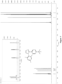
- a green emissive molecule is tris(2-phenylpyridine) iridium, denoted Ir(ppy) 3 , which has the following structure:
- organic includes polymeric materials as well as small molecule organic materials that may be used to fabricate organic opto-electronic devices.
- Small molecule refers to any organic material that is not a polymer, and "small molecules” may actually be quite large. Small molecules may include repeat units in some circumstances. For example, using a long chain alkyl group as a substituent does not remove a molecule from the "small molecule” class. Small molecules may also be incorporated into polymers, for example as a pendent group on a polymer backbone or as a part of the backbone. Small molecules may also serve as the core moiety of a dendrimer, which consists of a series of chemical shells built on the core moiety.
- the core moiety of a dendrimer may be a fluorescent or phosphorescent small molecule emitter.
- a dendrimer may be a "small molecule,” and it is believed that all dendrimers currently used in the field of OLEDs are small molecules.
- top means furthest away from the substrate, while “bottom” means closest to the substrate.
- first layer is described as “disposed over” a second layer, the first layer is disposed further away from substrate. There may be other layers between the first and second layer, unless it is specified that the first layer is "in contact with” the second layer.
- a cathode may be described as “disposed over” an anode, even though there are various organic layers in between.
- solution processable means capable of being dissolved, dispersed, or transported in and/or deposited from a liquid medium, either in solution or suspension form.
- a ligand may be referred to as "photoactive” when it is believed that the ligand directly contributes to the photoactive properties of an emissive material.
- a ligand may be referred to as "ancillary” when it is believed that the ligand does not contribute to the photoactive properties of an emissive material, although an ancillary ligand may alter the properties of a photoactive ligand.
- a first "Highest Occupied Molecular Orbital” (HOMO) or “Lowest Unoccupied Molecular Orbital” (LUMO) energy level is “greater than” or "higher than” a second HOMO or LUMO energy level if the first energy level is closer to the vacuum energy level.
- IP ionization potentials
- a higher HOMO energy level corresponds to an IP having a smaller absolute value (an IP that is less negative).
- a higher LUMO energy level corresponds to an electron affinity (EA) having a smaller absolute value (an EA that is less negative).
- the LUMO energy level of a material is higher than the HOMO energy level of the same material.
- a "higher” HOMO or LUMO energy level appears closer to the top of such a diagram than a "lower” HOMO or LUMO energy level.
- a first work function is "greater than” or “higher than” a second work function if the first work function has a higher absolute value. Because work functions are generally measured as negative numbers relative to vacuum level, this means that a "higher” work function is more negative. On a conventional energy level diagram, with the vacuum level at the top, a “higher” work function is illustrated as further away from the vacuum level in the downward direction. Thus, the definitions of HOMO and LUMO energy levels follow a different convention than work functions.
- US 2005/116626 A1 discloses iridium complexes and light emitting devices comprising iridium complexes as phosphorescent bodies.
- US 2010/176386 A1 describes the use of metal complexes containing bulky carborane-containing auxiliary ligands in organic electronic devices.
- US 2017/352822 A1 discloses a platinum complex, an OLED using the platinum complex, and an apparatus emitting visible light or near-IR light.
- JP 2012006878 A describes iridium complexes to be used as phosphorescent dopants in OLEDs.
- the present disclosure relates to an electroluminescent compound having a surface region of highly negative electrostatic potential
- An OLED comprising the compound of the present disclosure in an organic layer therein is also disclosed.
- a consumer product comprising the OLED is also disclosed.
- a formulation comprising the compound of the present disclosure is also disclosed.
- an OLED comprises at least one organic layer disposed between and electrically connected to an anode and a cathode.
- the anode injects holes and the cathode injects electrons into the organic layer(s).
- the injected holes and electrons each migrate toward the oppositely charged electrode.
- an "exciton” which is a localized electron-hole pair having an excited energy state, is formed.
- Light is emitted when the exciton relaxes via a photoemissive mechanism.
- the exciton may be localized on an excimer or an exciplex. Non-radiative mechanisms, such as thermal relaxation, may also occur, but are generally considered undesirable.
- the initial OLEDs used emissive molecules that emitted light from their singlet states ("fluorescence") as disclosed, for example, in U.S. Pat. No. 4,769,292 . Fluorescent emission generally occurs in a time frame of less than 10 nanoseconds.
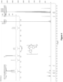
- FIG. 1 shows an organic light emitting device 100.
- Device 100 may include a substrate 110, an anode 115, a hole injection layer 120, a hole transport layer 125, an electron blocking layer 130, an emissive layer 135, a hole blocking layer 140, an electron transport layer 145, an electron injection layer 150, a protective layer 155, a cathode 160, and a barrier layer 170.
- Cathode 160 is a compound cathode having a first conductive layer 162 and a second conductive layer 164.
- Device 100 may be fabricated by depositing the layers described, in order. The properties and functions of these various layers, as well as example materials, are described in more detail in US 7,279,704 at cols. 6-10.
- a flexible and transparent substrate-anode combination is disclosed in U.S. Pat. No. 5,844,363 .
- An example of a p-doped hole transport layer is m-MTDATA doped with F 4 -TCNQ at a molar ratio of 50:1, as disclosed in U.S. Patent Application Publication No. 2003/0230980 .
- Examples of emissive and host materials are disclosed in U.S. Pat. No. 6,303,238 to Thompson et al. .
- An example of an n-doped electron transport layer is BPhen doped with Li at a molar ratio of 1:1, as disclosed in U.S. Patent Application Publication No. 2003/0230980 .
- U.S. Pat. Nos. 5,703,436 and 5,707,745 disclose examples of cathodes including compound cathodes having a thin layer of metal such as Mg:Ag with an overlying transparent, electrically-conductive, sputter-deposited ITO layer.
- the theory and use of blocking layers is described in more detail in U.S. Pat. No. 6,097,147 and U.S. Patent Application Publication No. 2003/0230980 .
- Examples of injection layers are provided in U.S. Patent Application Publication No. 2004/0174116 .
- a description of protective layers may be found in U.S. Patent Application Publication No. 2004/0174116 .
- FIG. 2 shows an inverted OLED 200.
- the device includes a substrate 210, a cathode 215, an emissive layer 220, a hole transport layer 225, and an anode 230.
- Device 200 may be fabricated by depositing the layers described, in order. Because the most common OLED configuration has a cathode disposed over the anode, and device 200 has cathode 215 disposed under anode 230, device 200 may be referred to as an "inverted" OLED. Materials similar to those described with respect to device 100 may be used in the corresponding layers of device 200.
- FIG. 2 provides one example of how some layers may be omitted from the structure of device 100.
- FIGS. 1 and 2 The simple layered structure illustrated in FIGS. 1 and 2 is provided by way of non-limiting example, and it is understood that embodiments of the invention may be used in connection with a wide variety of other structures.
- the specific materials and structures described are exemplary in nature, and other materials and structures may be used.
- Functional OLEDs may be achieved by combining the various layers described in different ways, or layers may be omitted entirely, based on design, performance, and cost factors. Other layers not specifically described may also be included. Materials other than those specifically described may be used. Although many of the examples provided herein describe various layers as comprising a single material, it is understood that combinations of materials, such as a mixture of host and dopant, or more generally a mixture, may be used. Also, the layers may have various sublayers.
- hole transport layer 225 transports holes and injects holes into emissive layer 220, and may be described as a hole transport layer or a hole injection layer.
- an OLED may be described as having an "organic layer" disposed between a cathode and an anode. This organic layer may comprise a single layer, or may further comprise multiple layers of different organic materials as described, for example, with respect to FIGS. 1 and 2 .
- OLEDs comprised of polymeric materials (PLEDs) such as disclosed in U.S. Pat. No. 5,247,190 to Friend et al. .
- PLEDs polymeric materials
- OLEDs having a single organic layer may be used.
- OLEDs may be stacked, for example as described in U.S. Pat. No. 5,707,745 to Forrest et al.
- the OLED structure may deviate from the simple layered structure illustrated in FIGS. 1 and 2 .
- the substrate may include an angled reflective surface to improve out-coupling, such as a mesa structure as described in U.S. Pat. No. 6,091,195 to Forrest et al. , and/or a pit structure as described in U.S. Pat. No. 5,834,893 to Bulovic et al. .
- any of the layers of the various embodiments may be deposited by any suitable method.
- preferred methods include thermal evaporation, ink-jet, such as described in U.S. Pat. Nos. 6,013,982 and 6,087,196 organic vapor phase deposition (OVPD), such as described in U.S. Pat. No. 6,337,102 to Forrest et al. and deposition by organic vapor jet printing (OVJP), such as described in U.S. Pat. No. 7,431,968 .
- OVPD organic vapor phase deposition
- OJP organic vapor jet printing
- Other suitable deposition methods include spin coating and other solution based processes. Solution based processes are preferably carried out in nitrogen or an inert atmosphere.
- preferred methods include thermal evaporation.
- Preferred patterning methods include deposition through a mask, cold welding such as described in U.S. Pat. Nos. 6,294,398 and 6,468,819 and patterning associated with some of the deposition methods such as ink-jet and organic vapor jet printing (OVJP). Other methods may also be used.
- the materials to be deposited may be modified to make them compatible with a particular deposition method.
- substituents such as alkyl and aryl groups, branched or unbranched, and preferably containing at least 3 carbons, may be used in small molecules to enhance their ability to undergo solution processing. Substituents having 20 carbons or more may be used, and 3-20 carbons is a preferred range. Materials with asymmetric structures may have better solution processability than those having symmetric structures, because asymmetric materials may have a lower tendency to recrystallize. Dendrimer substituents may be used to enhance the ability of small molecules to undergo solution processing.
- Devices fabricated in accordance with embodiments of the present invention may further optionally comprise a barrier layer.
- a barrier layer One purpose of the barrier layer is to protect the electrodes and organic layers from damaging exposure to harmful species in the environment including moisture, vapor and/or gases, etc.
- the barrier layer may be deposited over, under or next to a substrate, an electrode, or over any other parts of a device including an edge.
- the barrier layer may comprise a single layer, or multiple layers.
- the barrier layer may be formed by various known chemical vapor deposition techniques and may include compositions having a single phase as well as compositions having multiple phases. Any suitable material or combination of materials may be used for the barrier layer.
- the barrier layer may incorporate an inorganic or an organic compound or both.
- the preferred barrier layer comprises a mixture of a polymeric material and a non-polymeric material as described in U.S. Pat. No. 7,968,146 , PCT Pat. Application Nos. PCT/US2007/023098 and PCT/US2009/042829 .
- the aforesaid polymeric and non-polymeric materials comprising the barrier layer should be deposited under the same reaction conditions and/or at the same time.
- the weight ratio of polymeric to non-polymeric material may be in the range of 95:5 to 5:95.
- the polymeric material and the non-polymeric material may be created from the same precursor material.
- the mixture of a polymeric material and a non-polymeric material consists essentially of polymeric silicon and inorganic silicon.
- Devices fabricated in accordance with embodiments of the invention can be incorporated into a wide variety of electronic component modules (or units) that can be incorporated into a variety of electronic products or intermediate components. Examples of such electronic products or intermediate components include display screens, lighting devices such as discrete light source devices or lighting panels, etc. that can be utilized by the end-user product manufacturers. Such electronic component modules can optionally include the driving electronics and/or power source(s). Devices fabricated in accordance with embodiments of the invention can be incorporated into a wide variety of consumer products that have one or more of the electronic component modules (or units) incorporated therein.
- a consumer product comprising an OLED that includes the compound of the present disclosure in the organic layer in the OLED is disclosed.
- Such consumer products would include any kind of products that include one or more light source(s) and/or one or more of some type of visual displays.
- Some examples of such consumer products include flat panel displays, curved displays, computer monitors, medical monitors, televisions, billboards, lights for interior or exterior illumination and/or signaling, heads-up displays, fully or partially transparent displays, flexible displays, rollable displays, foldable displays, stretchable displays, laser printers, telephones, mobile phones, tablets, phablets, personal digital assistants (PDAs), wearable devices, laptop computers, digital cameras, camcorders, viewfinders, micro-displays (displays that are less than 2 inches diagonal), 3-D displays, virtual reality or augmented reality displays, vehicles, video walls comprising multiple displays tiled together, theater or stadium screen, a light therapy device, and a sign.
- control mechanisms may be used to control devices fabricated in accordance with the present invention, including passive matrix and active matrix. Many of the devices are intended for use in a temperature range comfortable to humans, such as 18 degrees C. to 30 degrees C., and more preferably at room temperature (20-25 degrees C), but could be used outside this temperature range, for example, from -40 degree C to + 80 degree C.
- the materials and structures described herein may have applications in devices other than OLEDs.
- other optoelectronic devices such as organic solar cells and organic photodetectors may employ the materials and structures.
- organic devices such as organic transistors, may employ the materials and structures.
- halo halogen
- halide halogen
- fluorine chlorine, bromine, and iodine
- acyl refers to a substituted carbonyl radical (C(O)-R s ).
- esters refers to a substituted oxycarbonyl (-O-C(O)-R s or -C(O)-O-R s ) radical.
- ether refers to an -OR s radical.
- sulfanyl or "thio-ether” are used interchangeably and refer to a -SR s radical.
- sulfinyl refers to a -S(O)-R s radical.
- sulfonyl refers to a -SO 2 -R, radical.
- phosphino refers to a -P(R s ) 3 radical, wherein each R s can be same or different.
- sil refers to a -Si(R s ) 3 radical, wherein each R s can be same or different.
- R s can be hydrogen or a substituent selected from the group consisting of deuterium, halogen, alkyl, cycloalkyl, heteroalkyl, heterocycloalkyl, arylalkyl, alkoxy, aryloxy, amino, silyl, alkenyl, cycloalkenyl, heteroalkenyl, alkynyl, aryl, heteroaryl, and combination thereof.
- Preferred R s is selected from the group consisting of alkyl, cycloalkyl, aryl, heteroaryl, and combination thereof.
- alkyl refers to and includes both straight and branched chain alkyl radicals.
- Preferred alkyl groups are those containing from one to fifteen carbon atoms and includes methyl, ethyl, propyl, 1-methylethyl, butyl, 1-methylpropyl, 2-methylpropyl, pentyl, 1-methylbutyl, 2-methylbutyl, 3-methylbutyl, 1,1-dimethylpropyl, 1,2-dimethylpropyl, 2,2-dimethylpropyl. Additionally, the alkyl group is optionally substituted.
- cycloalkyl refers to and includes monocyclic, polycyclic, and spiro alkyl radicals.
- Preferred cycloalkyl groups are those containing 3 to 12 ring carbon atoms and includes cyclopropyl, cyclopentyl, cyclohexyl, bicyclo[3.1. 1]heptyl, spiro[4.5]decyl, spiro[5.5]undecyl, adamantyl. Additionally, the cycloalkyl group is optionally substituted.
- heteroalkyl or “heterocycloalkyl” refer to an alkyl or a cycloalkyl radical, respectively, having at least one carbon atom replaced by a heteroatom.
- the at least one heteroatom is selected from O, S, N, P, B, Si and Se, preferably, O, S or N.
- the heteroalkyl or heterocycloalkyl group is optionally substituted.
- alkenyl refers to and includes both straight and branched chain alkene radicals.
- Alkenyl groups are essentially alkyl groups that include at least one carbon-carbon double bond in the alkyl chain.
- Cycloalkenyl groups are essentially cycloalkyl groups that include at least one carbon-carbon double bond in the cycloalkyl ring.
- heteroalkenyl refers to an alkenyl radical having at least one carbon atom replaced by a heteroatom.
- the at least one heteroatom is selected from O, S, N, P, B, Si, and Se, preferably, O, S, or N.
- Preferred alkenyl, cycloalkenyl, or heteroalkenyl groups are those containing two to fifteen carbon atoms. Additionally, the alkenyl, cycloalkenyl, or heteroalkenyl group is optionally substituted.
- alkynyl refers to and includes both straight and branched chain alkyne radicals. Preferred alkynyl groups are those containing two to fifteen carbon atoms. Additionally, the alkynyl group is optionally substituted.
- aralkyl or “arylalkyl” are used interchangeably and refer to an alkyl group that is substituted with an aryl group. Additionally, the aralkyl group is optionally substituted.
- heterocyclic group refers to and includes aromatic and non-aromatic cyclic radicals containing at least one heteroatom.
- the at least one heteroatom is selected from O, S, N, P, B, Si, and Se, preferably, O, S, or N.
- Hetero-aromatic cyclic radicals may be used interchangeably with heteroaryl.
- Preferred hetero-non-aromatic cyclic groups are those containing 3 to 7 ring atoms which includes at least one hetero atom, and includes cyclic amines such as morpholino, piperidino, pyrrolidino, and cyclic ethers/thio-ethers, such as tetrahydrofuran, tetrahydropyran, tetrahydrothiophene. Additionally, the heterocyclic group may be optionally substituted.
- aryl refers to and includes both single-ring aromatic hydrocarbyl groups and polycyclic aromatic ring systems.
- the polycyclic rings may have two or more rings in which two carbons are common to two adjoining rings (the rings are "fused") wherein at least one of the rings is an aromatic hydrocarbyl group, e.g., the other rings can be cycloalkyls, cycloalkenyls, aryl, heterocycles, and/or heteroaryls.
- Preferred aryl groups are those containing six to thirty carbon atoms, preferably six to twenty carbon atoms, more preferably six to twelve carbon atoms. Especially preferred is an aryl group having six carbons, ten carbons or twelve carbons.
- Suitable aryl groups include phenyl, biphenyl, triphenyl, triphenylene, tetraphenylene, naphthalene, anthracene, phenalene, phenanthrene, fluorene, pyrene, chrysene, perylene, and azulene, preferably phenyl, biphenyl, triphenyl, triphenylene, fluorene, and naphthalene. Additionally, the aryl group is optionally substituted.
- heteroaryl refers to and includes both single-ring aromatic groups and polycyclic aromatic ring systems that include at least one heteroatom.
- the heteroatoms include O, S, N, P, B, Si, and Se. In many instances, O, S, or N are the preferred heteroatoms.
- Hetero-single ring aromatic systems are preferably single rings with 5 or 6 ring atoms, and the ring can have from one to six heteroatoms.
- the hetero-polycyclic ring systems can have two or more rings in which two atoms are common to two adjoining rings (the rings are "fused") wherein at least one of the rings is a heteroaryl, e.g., the other rings can be cycloalkyls, cycloalkenyls, aryl, heterocycles, and/or heteroaryls.
- the hetero-polycyclic aromatic ring systems can have from one to six heteroatoms per ring of the polycyclic aromatic ring system.
- Preferred heteroaryl groups are those containing three to thirty carbon atoms, preferably three to twenty carbon atoms, more preferably three to twelve carbon atoms.
- Suitable heteroaryl groups include dibenzothiophene, dibenzofuran, dibenzoselenophene, furan, thiophene, benzofuran, benzothiophene, benzoselenophene, carbazole, indolocarbazole, pyridylindole, pyrrolodipyridine, pyrazole, imidazole, triazole, oxazole, thiazole, oxadiazole, oxatriazole, dioxazole, thiadiazole, pyridine, pyridazine, pyrimidine, pyrazine, triazine, oxazine, oxathiazine, oxadiazine, indole, benzimidazole, indazole, indoxazine, benzoxazole, benzisoxazole, benzothiazole, quinoline, isoquinoline, cinnoline, qui
- aryl and heteroaryl groups listed above the groups of triphenylene, naphthalene, anthracene, dibenzothiophene, dibenzofuran, dibenzoselenophene, carbazole, indolocarbazole, imidazole, pyridine, pyrazine, pyrimidine, triazine, and benzimidazole, and the respective aza-analogs of each thereof are of particular interest.
- alkyl, cycloalkyl, heteroalkyl, heterocycloalkyl, alkenyl, cycloalkenyl, heteroalkenyl, alkynyl, aralkyl, heterocyclic group, aryl, and heteroaryl, as used herein, are independently unsubstituted, or independently substituted, with one or more general substituents.
- the general substituents are selected from the group consisting of deuterium, halogen, alkyl, cycloalkyl, heteroalkyl, heterocycloalkyl, arylalkyl, alkoxy, aryloxy, amino, silyl, alkenyl, cycloalkenyl, heteroalkenyl, alkynyl, aryl, heteroaryl, acyl, carboxylic acid, ether, ester, nitrile, isonitrile, sulfanyl, sulfinyl, sulfonyl, phosphino, and combinations thereof.
- the preferred general substituents are selected from the group consisting of deuterium, fluorine, alkyl, cycloalkyl, heteroalkyl, alkoxy, aryloxy, amino, silyl, alkenyl, cycloalkenyl, heteroalkenyl, aryl, heteroaryl, nitrile, isonitrile, sulfanyl, and combinations thereof.
- the preferred general substituents are selected from the group consisting of deuterium, fluorine, alkyl, cycloalkyl, alkoxy, aryloxy, amino, silyl, aryl, heteroaryl, sulfanyl, and combinations thereof.
- the more preferred general substituents are selected from the group consisting of deuterium, fluorine, alkyl, cycloalkyl, aryl, heteroaryl, and combinations thereof.
- substituted and substitution refer to a substituent other than H that is bonded to the relevant position, e.g., a carbon or nitrogen.
- R 1 when R 1 represents monosubstitution, then one R 1 must be other than H (i.e., a substitution). Similarly, when R 1 represents disubstitution, then two of R 1 must be other than H.
- R 1 when R 1 represents no substitution, R 1 , for example, can be a hydrogen for available valencies of ring atoms, as in carbon atoms for benzene and the nitrogen atom in pyrrole, or simply represents nothing for ring atoms with fully filled valencies, e.g., the nitrogen atom in pyridine.
- the maximum number of substitutions possible in a ring structure will depend on the total number of available valencies in the ring atoms.
- substitution includes a combination of two to four of the listed groups.
- substitution includes a combination of two to three groups.
- substitution includes a combination of two groups.
- Preferred combinations of substituent groups are those that contain up to fifty atoms that are not hydrogen or deuterium, or those which include up to forty atoms that are not hydrogen or deuterium, or those that include up to thirty atoms that are not hydrogen or deuterium. In many instances, a preferred combination of substituent groups will include up to twenty atoms that are not hydrogen or deuterium.
- aza-dibenzofuran i.e. aza-dibenzofuran, aza-dibenzothiophene, etc.
- azatriphenylene encompasses both dibenzo[ f,h ]quinoxaline and dibenzo[ f , h ]quinoline.
- deuterium refers to an isotope of hydrogen.
- Deuterated compounds can be readily prepared using methods known in the art. For example, U.S. Pat. No. 8,557,400 , Patent Pub. No. WO 2006/095951 , and U.S. Pat. Application Pub. No. US 2011/0037057 describe the making of deuterium-substituted organometallic complexes. Further reference is made to Ming Yan, et al., Tetrahedron 2015, 71, 1425-30 and Atzrodt et al., Angew. Chem. Int. Ed. (Reviews) 2007, 46, 7744-65 describe the deuteration of the methylene hydrogens in benzyl amines and efficient pathways to replace aromatic ring hydrogens with deuterium, respectively.
- a pair of adjacent substituents can be optionally joined or fused into a ring.
- the preferred ring is a five, six, or seven-membered carbocyclic or heterocyclic ring, includes both instances where the portion of the ring formed by the pair of substituents is saturated and where the portion of the ring formed by the pair of substituents is unsaturated.
- "adjacent" means that the two substituents involved can be on the same ring next to each other, or on two neighboring rings having the two closest available substitutable positions, such as 2, 2' positions in a biphenyl, or 1, 8 position in a naphthalene, as long as they can form a stable fused ring system.
- the present disclosure relates to an electroluminescent compound having a surface region of highly negative electrostatic potential
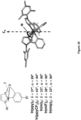
- the compound has the formula M(L A ) x (L B ) y , where x is 1, 2, or 3; y is 0, 1, or 2; and x + y is the oxidation state of the metal.
- the optional ligand L B is bidentate.
- the optional ligand L B is monoanionic.
- each of the ligands L B can be the same as, or different from, each other ligand L B .
- the ligand L A has a different structure from the ligand L B .
- the ligand L B does not include a perfluoroalkyl or perfluoroaryl group.
- the metal M is selected from the group consisting of Re, Os, Rh, Ir, Pd, Pt, Ag, Ag, and Cu.
- the metal M is selected from Os, Ru, Ir, or Rh.
- the ligand L A is bidentate, and the coordination to the metal includes one, two, or three ligand(s) L A .
- the metal M is also coordinated to one or more additional ligand L B .
- the metal M is selected from Pt or Pd.
- the coordination to the metal includes one or two ligand(s) L A . In one embodiment, if there are two ligands L A . In one embodiment, the compound comprises one ligand L A and one optional ligand L B .
- the compound has the formula Ir(L A ) 3 . In one embodiment, the compound having the formula Ir(L A ) 3 is the facial ( fac ) isomer. In one embodiment, the compound has a neutral charge.
- the compound comprises a surface region of high electrostatic potential (ESP).
- the region of high ESP comprises a region of very negative ESP.
- the ESP of the compound is non-uniform.
- the most negative ESPs of the compound are symmetrically disposed around the C 3 axis.
- the negative ESP of the compound forms a patch of high ESP.
- the patch of high ESP reinforces an alignment of the molecule that favors a low anisotropy factor.
- the patch of high ESP has a lower affinity for the surface of the host matrix.
- the lower affinity of the region of high ESP is caused by a decrease in van der Waals interactions.
- the region of high ESP reinforces horizontal alignment during deposition of the compound.
- a formulation comprising the compound described herein is also disclosed.
- the present disclosure relates to an organic electroluminescent device (OLED) comprising an anode; a cathode; and an organic layer, disposed between the anode and the cathode, comprising a compound of the present disclosure.
- OLED organic electroluminescent device
- the OLED has one or more characteristics selected from the group consisting of being flexible, being rollable, being foldable, being stretchable, and being curved. In some embodiments, the OLED is transparent or semi-transparent. In some embodiments, the OLED further comprises a layer comprising carbon nanotubes.
- the OLED further comprises a layer comprising a delayed fluorescent emitter.
- the OLED comprises a RGB pixel arrangement or white plus color filter pixel arrangement.
- the OLED is a mobile device, a hand held device, or a wearable device.
- the OLED is a display panel having less than 10 inch diagonal or 50 square inch area.
- the OLED is a display panel having at least 10 inch diagonal or 50 square inch area.
- the OLED is a lighting panel.
- the compound can be an emissive dopant.
- the compound can produce emissions via phosphorescence, fluorescence, thermally activated delayed fluorescence, i.e., TADF (also referred to as E-type delayed fluorescence; see, e.g., U.S. Application No. 15/700,352 ), triplet-triplet annihilation, or combinations of these processes.
- the emissive dopant can be a racemic mixture, or can be enriched in one enantiomer.
- the compound is neutrally charged.
- the compound can be homoleptic (each ligand is the same).
- the compound can be heteroleptic (at least one ligand is different from others).
- the ligands can all be the same in some embodiments.
- at least one ligand is different from the other ligands.
- every ligand can be different from each other. This is also true in embodiments where a ligand being coordinated to a metal can be linked with other ligands being coordinated to that metal to form a tridentate, tetradentate, pentadentate, or hexadentate ligands.
- the coordinating ligands are being linked together, all of the ligands can be the same in some embodiments, and at least one of the ligands being linked can be different from the other ligand(s) in some other embodiments.
- the compound can be used as a phosphorescent sensitizer in an OLED where one or multiple layers in the OLED contains an acceptor in the form of one or more fluorescent and/or delayed fluorescence emitters.
- the compound can be used as one component of an exciplex to be used as a sensitizer.
- the compound must be capable of energy transfer to the acceptor and the acceptor will emit the energy or further transfer energy to a final emitter.
- the acceptor concentrations can range from 0.001% to 100%.
- the acceptor could be in either the same layer as the phosphorescent sensitizer or in one or more different layers.
- the acceptor is a TADF emitter.
- the acceptor is a fluorescent emitter.
- the emission can arise from any or all of the sensitizer, acceptor, and final emitter.
- the OLED disclosed herein can be incorporated into one or more of a consumer product, an electronic component module, and a lighting panel.
- the organic layer can be an emissive layer and the compound can be an emissive dopant in some embodiments, while the compound can be a non-emissive dopant in other embodiments.
- the organic layer can also include a host.
- a host In some embodiments, two or more hosts are preferred.
- the hosts used maybe a) bipolar, b) electron transporting, c) hole transporting or d) wide band gap materials that play little role in charge transport.
- the host can include a metal complex.
- the host can be a triphenylene containing benzo-fused thiophene or benzo-fused furan.
- n can range from 1 to 10; and Ar 1 and Ar 2 can be independently selected from the group consisting of benzene, biphenyl, naphthalene, triphenylene, carbazole, and heteroaromatic analogs thereof.
- the host can be an inorganic compound.
- a Zn containing inorganic material e.g. ZnS.
- the host can be a compound comprising at least one chemical group selected from the group consisting of triphenylene, carbazole, dibenzothiophene, dibenzofuran, dibenzoselenophene, azatriphenylene, azacarbazole, aza-dibenzothiophene, aza-dibenzofuran, and aza-dibenzoselenophene.
- the host can include a metal complex.
- the host can be a specific compound selected from the group consisting of: and combinations thereof. Additional information on possible hosts is provided below.
- a formulation that comprises the novel compound disclosed herein is described.
- the formulation can include one or more components selected from the group consisting of a solvent, a host, a hole injection material, hole transport material, electron blocking material, hole blocking material, and an electron transport material, disclosed herein.
- the materials described herein as useful for a particular layer in an organic light emitting device may be used in combination with a wide variety of other materials present in the device.
- emissive dopants disclosed herein may be used in conjunction with a wide variety of hosts, transport layers, blocking layers, injection layers, electrodes and other layers that may be present.
- the materials described or referred to below are non-limiting examples of materials that may be useful in combination with the compounds disclosed herein, and one of skill in the art can readily consult the literature to identify other materials that may be useful in combination.
- a charge transport layer can be doped with conductivity dopants to substantially alter its density of charge carriers, which will in turn alter its conductivity.
- the conductivity is increased by generating charge carriers in the matrix material, and depending on the type of dopant, a change in the Fermi level of the semiconductor may also be achieved.
- Hole-transporting layer can be doped by p-type conductivity dopants and n-type conductivity dopants are used in the electron-transporting layer.
- Non-limiting examples of the conductivity dopants that may be used in an OLED in combination with materials disclosed herein are exemplified below together with references that disclose those materials: EP01617493 , EP01968131 , EP2020694 , EP2684932 , US20050139810 , US20070160905 , US20090167167 , US2010288362 , WO06081780 , WO2009003455 , WO2009008277 , WO2009011327 , WO2014009310 , US2007252140 , US2015060804 , US20150123047 , and US2012146012 .
- a hole injecting/transporting material to be used in the present invention is not particularly limited, and any compound may be used as long as the compound is typically used as a hole injecting/transporting material.
- the material include: a phthalocyanine or porphyrin derivative; an aromatic amine derivative; an indolocarbazole derivative; a polymer containing fluorohydrocarbon; a polymer with conductivity dopants; a conducting polymer, such as PEDOT/PSS; a self-assembly monomer derived from compounds such as phosphonic acid and silane derivatives; a metal oxide derivative, such as MoO x ; a p-type semiconducting organic compound, such as 1,4,5,8,9,12-Hexaazatriphenylenehexacarbonitrile; a metal complex, and a cross-linkable compounds.
- aromatic amine derivatives used in HIL or HTL include the following general structures:
- Each of Ar 1 to Ar 9 is selected from the group consisting of aromatic hydrocarbon cyclic compounds such as benzene, biphenyl, triphenyl, triphenylene, naphthalene, anthracene, phenalene, phenanthrene, fluorene, pyrene, chrysene, perylene, and azulene; the group consisting of aromatic heterocyclic compounds such as dibenzothiophene, dibenzofuran, dibenzoselenophene, furan, thiophene, benzofuran, benzothiophene, benzoselenophene, carbazole, indolocarbazole, pyridylindole, pyrrolodipyridine, pyrazole, imidazole, triazole, oxazole, thiazole, oxadiazole, oxatriazole, dioxazole, thiadiazole, pyridine, pyridazine
- Each Ar may be unsubstituted or may be substituted by a substituent selected from the group consisting of deuterium, halogen, alkyl, cycloalkyl, heteroalkyl, heterocycloalkyl, arylalkyl, alkoxy, aryloxy, amino, silyl, alkenyl, cycloalkenyl, heteroalkenyl, alkynyl, aryl, heteroaryl, acyl, carboxylic acids, ether, ester, nitrile, isonitrile, sulfanyl, sulfinyl, sulfonyl, phosphino, and combinations thereof.
- a substituent selected from the group consisting of deuterium, halogen, alkyl, cycloalkyl, heteroalkyl, heterocycloalkyl, arylalkyl, alkoxy, aryloxy, amino, silyl, alkenyl, cycloalkenyl, heteroalkeny
- Ar 1 to Ar 9 is independently selected from the group consisting of: wherein k is an integer from 1 to 20; X 101 to X 108 is C (including CH) or N; Z 101 is NAr 1 , O, or S; Ar 1 has the same group defined above.
- Examples of metal complexes used in HIL or HTL include the following general formula: wherein Met is a metal, which can have an atomic weight greater than 40; (Y 101 -Y 102 ) is a bidentate ligand, Y 101 and Y 102 are independently selected from C, N, O, P, and S; L 101 is an ancillary ligand; k' is an integer value from 1 to the maximum number of ligands that may be attached to the metal; and k'+k" is the maximum number of ligands that may be attached to the metal.
- (Y 101 -Y 102 ) is a 2-phenylpyridine derivative. In another aspect, (Y 101 -Y 102 ) is a carbene ligand. In another aspect, Met is selected from Ir, Pt, Os, and Zn. In a further aspect, the metal complex has a smallest oxidation potential in solution vs. Fc + /Fc couple less than about 0.6 V.
- Non-limiting examples of the HIL and HTL materials that may be used in an OLED in combination with materials disclosed herein are exemplified below together with references that disclose those materials: CN102702075 , DE102012005215 , EP01624500 , EP01698613 , EP01806334 , EP01930964 , EP01972613 , EP01997799 , EP02011790 , EP02055700 , EP02055701 , EP1725079 , EP2085382 , EP2660300 , EP650955 , JP07-073529 , JP2005112765 , JP2007091719 , JP2008021687 , JP2014-009196 , KR20110088898 , KR20130077473 , TW201139402 , US06517957 , US20020158242 , US20030162053 , US20050123751 , US20060182993 , US200602402
- An electron blocking layer may be used to reduce the number of electrons and/or excitons that leave the emissive layer.
- the presence of such a blocking layer in a device may result in substantially higher efficiencies, and/or longer lifetime, as compared to a similar device lacking a blocking layer.
- a blocking layer may be used to confine emission to a desired region of an OLED.
- the EBL material has a higher LUMO (closer to the vacuum level) and/or higher triplet energy than the emitter closest to the EBL interface.
- the EBL material has a higher LUMO (closer to the vacuum level) and/or higher triplet energy than one or more of the hosts closest to the EBL interface.
- the compound used in EBL contains the same molecule or the same functional groups used as one of the hosts described below.
- the light emitting layer of the organic EL device of the present invention preferably contains at least a metal complex as light emitting material, and may contain a host material using the metal complex as a dopant material.
- the host material are not particularly limited, and any metal complexes or organic compounds may be used as long as the triplet energy of the host is larger than that of the dopant. Any host material may be used with any dopant so long as the triplet criteria is satisfied.
- Examples of metal complexes used as host are preferred to have the following general formula: wherein Met is a metal; (Y 103 -Y 104 ) is a bidentate ligand, Y 103 and Y 104 are independently selected from C, N, O, P, and S; L 101 is an another ligand; k' is an integer value from 1 to the maximum number of ligands that may be attached to the metal; and k'+k" is the maximum number of ligands that may be attached to the metal.
- the metal complexes are: wherein (O-N) is a bidentate ligand, having metal coordinated to atoms O and N.
- Met is selected from Ir and Pt.
- (Y 103 -Y 104 ) is a carbene ligand.
- the host compound contains at least one of the following groups selected from the group consisting of aromatic hydrocarbon cyclic compounds such as benzene, biphenyl, triphenyl, triphenylene, tetraphenylene, naphthalene, anthracene, phenalene, phenanthrene, fluorene, pyrene, chrysene, perylene, and azulene; the group consisting of aromatic heterocyclic compounds such as dibenzothiophene, dibenzofuran, dibenzoselenophene, furan, thiophene, benzofuran, benzothiophene, benzoselenophene, carbazole, indolocarbazole, pyridylindole, pyrrolodipyridine, pyrazole, imidazole, triazole, oxazole, thiazole, oxadiazole, oxatriazole, dioxazole, thiadia
- Each option within each group may be unsubstituted or may be substituted by a substituent selected from the group consisting of deuterium, halogen, alkyl, cycloalkyl, heteroalkyl, heterocycloalkyl, arylalkyl, alkoxy, aryloxy, amino, silyl, alkenyl, cycloalkenyl, heteroalkenyl, alkynyl, aryl, heteroaryl, acyl, carboxylic acids, ether, ester, nitrile, isonitrile, sulfanyl, sulfinyl, sulfonyl, phosphino, and combinations thereof.
- the host compound contains at least one of the following groups in the molecule: and wherein R 101 is selected from the group consisting of hydrogen, deuterium, halogen, alkyl, cycloalkyl, heteroalkyl, heterocycloalkyl, arylalkyl, alkoxy, aryloxy, amino, silyl, alkenyl, cycloalkenyl, heteroalkenyl, alkynyl, aryl, heteroaryl, acyl, carboxylic acids, ether, ester, nitrile, isonitrile, sulfanyl, sulfinyl, sulfonyl, phosphino, and combinations thereof, and when it is aryl or heteroaryl, it has the similar definition as Ar's mentioned above.
- k is an integer from 0 to 20 or 1 to 20.
- X 101 to X 108 are independently selected from C (including CH) or N.
- Z 101 and Z 102 are independently selected from NR 101
- Non-limiting examples of the host materials that may be used in an OLED in combination with materials disclosed herein are exemplified below together with references that disclose those materials: EP2034538 , EP2034538A , EP2757608 , JP2007254297 , KR20100079458 , KR20120088644 , KR20120129733 , KR20130115564 , TW201329200 , US20030175553 , US20050238919 , US20060280965 , US20090017330 , US20090030202 , US20090167162 , US20090302743 , US20090309488 , US20100012931 , US20100084966 , US20100187984 , US2010187984 , US2012075273 , US2012126221 , US2013009543 , US2013105787 , US2013175519 , US2014001446 , US20140183503 , US20140225088 ,
- One or more additional emitter dopants may be used in conjunction with the compound of the present disclosure.
- the additional emitter dopants are not particularly limited, and any compounds may be used as long as the compounds are typically used as emitter materials.
- suitable emitter materials include compounds, which can produce emissions via phosphorescence, fluorescence, thermally activated delayed fluorescence, i.e., TADF (also referred to as E-type delayed fluorescence), triplet-triplet annihilation, or combinations of these processes.
- Non-limiting examples of the emitter materials that may be used in an OLED in combination with materials disclosed herein are exemplified below together with references that disclose those materials: CN103694277 , CN1696137 , EB01238981 , EP01239526 , EP01961743 , EP1239526 , EP1244155 , EP1642951 , EP1647554 , EP1841834 , EP1841834B , EP2062907 , EP2730583 , JP2012074444 , JP2013110263 , JP4478555 , KR1020090133652 , KR20120032054 , KR20130043460 , TW201332980 , US06699599 , US06916554 , US20010019782 , US20020034656 , US20030068526 , US20030072964 , US20030138657 , US20050123788 , US20050244673 , US200512379
- a hole blocking layer may be used to reduce the number of holes and/or excitons that leave the emissive layer.
- the presence of such a blocking layer in a device may result in substantially higher efficiencies and/or longer lifetime as compared to a similar device lacking a blocking layer.
- a blocking layer may be used to confine emission to a desired region of an OLED.
- the HBL material has a lower HOMO (further from the vacuum level) and/or higher triplet energy than the emitter closest to the HBL interface.
- the HBL material has a lower HOMO (further from the vacuum level) and/or higher triplet energy than one or more of the hosts closest to the HBL interface.
- compound used in HBL contains the same molecule or the same functional groups used as host described above.
- compound used in HBL contains at least one of the following groups in the molecule: wherein k is an integer from 1 to 20; L 101 is an another ligand, k' is an integer from 1 to 3.
- Electron transport layer may include a material capable of transporting electrons. Electron transport layer may be intrinsic (undoped), or doped. Doping may be used to enhance conductivity. Examples of the ETL material are not particularly limited, and any metal complexes or organic compounds may be used as long as they are typically used to transport electrons.
- compound used in ETL contains at least one of the following groups in the molecule: wherein R 101 is selected from the group consisting of hydrogen, deuterium, halogen, alkyl, cycloalkyl, heteroalkyl, heterocycloalkyl, arylalkyl, alkoxy, aryloxy, amino, silyl, alkenyl, cycloalkenyl, heteroalkenyl, alkynyl, aryl, heteroaryl, acyl, carboxylic acids, ether, ester, nitrile, isonitrile, sulfanyl, sulfinyl, sulfonyl, phosphino, and combinations thereof, when it is aryl or heteroaryl, it has the similar definition as Ar's mentioned above.
- Ar 1 to Ar 3 has the similar definition as Ar's mentioned above.
- k is an integer from 1 to 20.
- X 101 to X 108 is selected from C (including CH) or N.
- the metal complexes used in ETL contains, but not limit to the following general formula: wherein (O-N) or (N-N) is a bidentate ligand, having metal coordinated to atoms O, N or N, N; L 101 is another ligand; k' is an integer value from 1 to the maximum number of ligands that may be attached to the metal.
- Non-limiting examples of the ETL materials that may be used in an OLED in combination with materials disclosed herein are exemplified below together with references that disclose those materials: CN103508940 , EP01602648 , EP01734038 , EP01956007 , JP2004-022334 , JP2005149918 , JP2005-268199 , KR0117693 , KR20130108183 , US20040036077 , US20070104977 , US2007018155 , US20090101870 , US20090115316 , US20090140637 , US20090179554 , US2009218940 , US2010108990 , US2011156017 , US2011210320 , US2012193612 , US2012214993 , US2014014925 , US2014014927 , US20140284580 , US6656612 , US8415031 , WO2003060956 , WO2007111263 , WO
- the CGL plays an essential role in the performance, which is composed of an n-doped layer and a p-doped layer for injection of electrons and holes, respectively. Electrons and holes are supplied from the CGL and electrodes. The consumed electrons and holes in the CGL are refilled by the electrons and holes injected from the cathode and anode, respectively; then, the bipolar currents reach a steady state gradually.
- Typical CGL materials include n and p conductivity dopants used in the transport layers.
- the hydrogen atoms can be partially or fully deuterated.
- any specifically listed substituent such as, without limitation, methyl, phenyl, pyridyl, etc. may be undeuterated, partially deuterated, and fully deuterated versions thereof.
- classes of substituents such as, without limitation, alkyl, aryl, cycloalkyl, heteroaryl, etc. also may be undeuterated, partially deuterated, and fully deuterated versions thereof.
- the orientation of facial ( fac ) tris -cyclometalated iridium complexes in doped films prepared by vacuum deposition is investigated by altering the physical shape and electronic asymmetry in the molecular structure.
- Angle-dependent photoluminescence spectroscopy and Fourier-plane imaging microscopy show that the orientation of roughly spherical fac- tris(2-phenylpyridyl)iridium (Ir(ppy) 3 ) is isotropic, whereas complexes that are oblate spheroids, fac -tris(mesityl-2-phenyl-1H-imidazole)iridium (Ir(mi) 3 ) and fac -tris((3,5-dimethyl-[1,1'-biphenyl]-4-yl)-2-phenyl-1H-imidazole)iridium (Ir(mip) 3 ), have a net horizontal alignment of their transition dipole moments.
- Optical anisotropy factors of 0.26 and 0.15, respectively, are obtained from the latter complexes when doped into tris (4-(9H-carbazol-9-yl)phenyl)amine host thin films.
- the horizontal alignment is attributed to the favorable van der Waals interaction between the oblate Ir complexes and host material.
- Trifluoromethyl groups substituted on one polar face of the Ir(ppy) 3 and Ir(mi) 3 complexes introduce chemical asymmetries in the molecules at the expense of their oblate shapes.
- the anisotropy factors of films doped with these substituted derivatives are lower relative to the parent complexes, indicating that the fluorinated patches reinforce horizontal alignment during deposition.
- High efficiencies obtained from organic light emitting diodes prepared using the Ir dopants are attributed, in part, to improved outcoupling of electroluminescence brought about by molecular alignment.
- OLEDs Organic light emitting diodes
- G. Hong, et al., Adv. Mater. 2021, 33 Even though 100% internal quantum efficiency has been achieved using phosphorescent dopants, fabrication of extremely high efficiency OLEDs has been hampered by relatively inefficient light extraction from the device ( W. Briitting, et al., physica status solidi (a) 2013, 210, 44 ; Y. Watanabe, et al., Bull. Chem. Soc. Jpn. 2019, 92, 716 ).
- TDMs transition dipole moments
- ⁇ the anisotropy factor
- Bis -cyclometalated Ir diketonate complexes are common emissive dopants in OLEDs that show anisotropy factors of 0.22-0.25 in vacuum deposited films, indicating a net in-plane TDM alignment ( C. K. Moon, et al., Nature Communications 2017, 8 ; T. Lee, et al., Nano Lett. 2017, 17, 6464 ).
- C ⁇ N octahedral (C ⁇ N) 2 Ir(L ⁇ X) type complexes
- Jurow et al. proposed that the organic/vacuum interface induces reorientation of dopants due to the inherent chemical asymmetries of the surface.
- C ⁇ N represents a cyclometalated ligand and L ⁇ X an auxiliary ligand ( M. J. Jurow, et al., Nature Materials 2016, 15, 85 ).
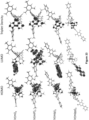
- Ir(ppy) 3 , Ir(ppyCF 3 ) 3 Ir(mi) 3 were prepared according to the literature procedure ( A. B. Tamayo, et al., Journal of the American Chemical Society 2003, 125, 7377 ; A. Singh, et al., J. Organomet. Chem. 2015, 776, 51 ; K. Udagawa, et al., Adv. Mater. 2014, 26, 5062 ; J. Y. Zhuang, et al., New J. Chem. 2015, 39, 246 ). Except for Ir(mipp) 3 , three compounds sublime with the reasonable yields (>50%), allowing for them to be employed in OLEDs.
- the reaction was cooled to ambient temperature and concentrated in vacuo to remove the methanol solvent.
- the crude mixture was diluted with ethyl acetate and treated with 1 M aqueous sodium hydroxide solution. The layers were then extracted and separated with water three times, and the resultant organic layer was then washed with brine, dried with sodium sulfate and concentrated in vacuo.
- the crude mixture was further purified by column chromatography (4:1 hexanes:ethyl acetate) to yield a pale yellow solid (1.67 g, 8.6%).
- Phosphoric acid (1.22 g, 12.5 mmol) was added after one hour and the reaction was left to reflux for an additional 24 hrs. The reaction was cooled to ambient temperature and concentrated in vacuo to remove the methanol solvent. The crude mixture was diluted with ethyl acetate and treated with 1 M aqueous sodium hydroxide solution. The layers were then extracted and separated with water three times and the resultant organic layer was then washed with brine, dried with sodium sulfate and concentrated in vacuo.
- the crude mixture was diluted with ethyl acetate and extracted with water three times, and the resultant organic layer was then washed with brine, dried with sodium sulfate and concentrated in vacuo.
- the crude mixture was further purified by column chromatography (4:1 hexanes:ethyl acetate) to yield a pale yellow solid (1.1 g, 36 %).
- Figure 8 provides a 1 H NMR spectrum of mipp-H in Acetone-d 6 .
- Figure 10 provides a 13 C NMR spectrum of Ir(mip) 3 in Acetone-d 6 : 13 C NMR (101 MHz, acetone) ⁇ 205.16, 156.43, 141.89, 139.85, 136.77, 136.41, 135.93, 131.95, 128.90, 127.78, 127.03, 126.98, 125.91, 120.30, 120.24, 17.21, 17.09.
- Figure 11 provides a 13 C NMR spectrum of Ir(miF) 3 in Acetone-d 6 : 13 C NMR (101 MHz, acetone) ⁇ 159.43, 140.09, 139.77, 135.67, 135.24, 133.35, 129.51, 129.41, 126.29, 121.61, 120.36, 115.91, 115.87, 20.27, 16.81, 16.42.
- Figure 12 provides a 13 C NMR spectrum of Ir(mipp) 3 in Acetone-d 6 : 13 C NMR (101 MHz, acetone) ⁇ 205.17, 160.48, 156.53, 141.29, 140.41, 140.28, 138.74, 137.46, 136.84, 136.48, 136.32, 136.01, 128.90, 127.53, 127.47, 127.38, 126.91, 126.76, 125.96, 120.69, 120.03, 118.27, 17.25, 17.13.
- Figure 13 provides a 13 C NMR spectrum of mip-H in Acetone-d 6 : 13 C NMR (101 MHz, acetone) ⁇ 141.44, 139.82, 135.96, 129.48, 128.87, 128.24, 128.03, 127.72, 127.01, 126.90, 126.55, 122.00, 17.01.
- Figure 14 provides a 13 C NMR spectrum of miF-H in Acetone-d 6 : 13 C NMR (101 MHz, acetone) ⁇ 139.14, 134.97, 129.85, 129.42, 126.72, 125.25, 125.21, 125.17, 125.14, 123.14, 20.18, 16.66.
- Figure 15 provides a 13 C NMR spectrum of mipp-H in Acetone-d 6 : 13 C NMR (101 MHz, acetone) ⁇ 205.18, 205.18, 205.16, 140.82, 140.32, 140.25, 138.70, 136.83, 136.02, 131.30, 129.48, 128.89, 128.24, 128.03, 127.48, 127.37, 127.32, 126.87, 126.74, 126.54, 122.00, 17.03.
- Figure 16 provides a 13 C NMR spectrum of 1-(4-bromo-2,6-dimethylphenyl)-2-phenyl-1 ⁇ 4 ,3 ⁇ 2 -imidazole in Acetone-d 6 : 13 C NMR (101 MHz, acetone) ⁇ 138.11, 136.78, 131.30, 130.98, 129.64, 128.31, 128.21, 126.58, 122.03, 121.80, 16.64.
- Photophysical Measurements Photoluminescence spectra were measured using a QuantaMaster Photon Technology International phosphorescence/fluorescence spectrofluorometer. Phosphorescent lifetimes were measured by time-correlated single-photon counting using an IBH Fluorocube instrument equipped with an LED excitation source. Quantum yield measurements were carried out using a Hamamatsu C9920 system equipped with a xenon lamp, calibrated integrating sphere and model C10027 photonic multi-channel analyzer (PMA). UV-vis spectra were recorded on a Hewlett-Packard 4853 diode array spectrometer. The samples were deaerated by extensive sparging with N 2 .
- PMA photonic multi-channel analyzer
- Table 1 Absorption data for the Ir complexes Ir(mi) 3 (1), Ir(miF) 3 (2), and Ir(mip) 3 (3) ⁇ max (nm) ( ⁇ , 10 3 M -1 cm -1 ) Ir(mi) 3 (1) 304 (10.7), 350 (12.6), 380 (sh, 8.13), 413 (sh, 3.47), 459 (sh, 0.461) Ir(miF) 3 (2) 353 (11.3), 386 (sh, 6.67), 428 (sh, 2.52), 473 (sh, 0.529) Ir(mip) 3 (3) 340 (14.8), 380 (sh, 9.25), 415 (sh, 3.86), 459 (sh, 0.722)
- LUMO of (1) and (3) are mainly located on mesityl and phenyl xylyl ligand respectively.
- the second phenyl group attached to mesityl imidazole ligand allows for the electrons to delocalize across extended xylyl phenyl backbone of the ligand, resulting in stabilization of the LUMO of (3).
- the 3D moments matrix of each complex was computed by taking the Ir atom as the center.
- ⁇ 1 , ⁇ 2 and ⁇ 3 represent the relative length of the principal semi-axes of a hypothetical ellipsoid hull that represents the molecule (i.e., a ⁇ ⁇ 1 , b ⁇ ⁇ 2 , c ⁇ ⁇ 3 ).
- the lengths of at least two of the semi-axes are expected to be similar ( a ⁇ b ).
- the aspect ratio can then be computed as the ratio between a and c.
- the DFT ground state optimized geometries were used to compute the aspect ratios in all cases; the results are shown in Table 2. Table 2.
- SOC-TDDFT spin-orbit coupling
- HOMO, LUMO, and triplet density of exemplary complexes are provided in Figure 23 .
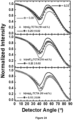
- Transition dipole moment vector (TDM) alignment measurements All thin films used in PL measurements were deposited at 0.9 ⁇ /s and 0.1 ⁇ /s for the host and dopant molecules, respectively, on 0.2 mm thick fused silica glass by vacuum thermal evaporation in a chamber with a base pressure of 1 ⁇ 10 -7 torr (1.33 . 10 -5 Pa). The deposition rate and thicknesses were controlled using a quartz crystal thickness monitor. Following the deposition, devices were encapsulated using an epoxy seal around the edge of a 1.57 mm thick cover glass in an ultrapure N 2 environment.
- TDM Transition dipole moment vector
- a motorized stage was used to position the detector. Simulations of the angular intensity profile are based on the dyadic Green's function in a birefringent medium ( K. Celebi, et al., Opt. Express 2007, 15, 1762 ). A least-squares algorithm was used to fit the experimental data to the simulation. The refractive indices and extinction coefficients of materials were measured using variable-angle spectroscopic ellipsometry.
- FPIM Fourier-plane imaging microscopy
- a long-pass filter was used to prevent the laser beam being incident on the CCD, while a band-pass filter with the pass band near the peak wavelength of the dopant photoluminescence was also placed in the optical path.
- a linear polarizer separates the emission into two the orthogonal planes corresponding to the p - and s - polarized plane modes. The obtained emission contour was fitted according to the reported method ( J. Kim, et al., Phys. Rev. Appl. 2020, 14, 034048 ).
- the k -space fitting was performed over a limited range of -1.1 ⁇ k x / k 0 ⁇ 1.1 ( J. A. Kurvits, et al., J. Opt. Soc. Am. A 2015, 32, 2082 ; J. A. Schuller, et al., Nat Nanotechnol 2013, 8, 271 ; M. A. Lieb, et al., J. Opt. Soc. Am. B 2004, 21, 1210 ; T. H. Taminiau, et al., Nat. Photonics 2008, 2, 234 ; M. Böhmler, et al., Opt. Express 2010, 18, 16443 ).
- OLED fabrication All thin films used in PL measurements were deposited at 0.9 ⁇ /s and 0.1 ⁇ /s for the host and dopant molecules, respectively, on 0.2 mm thick fused silica glass by vacuum thermal evaporation in a chamber with a base pressure of 1 ⁇ 10 -7 torr (1.33 ⁇ 10 -5 Pa). The deposition rate and thicknesses were controlled using a quartz crystal thickness monitor. Following the deposition, devices were encapsulated using an epoxy seal around the edge of a 1.57 mm thick cover glass in an ultrapure N 2 environment. PhOLEDs were grown by vacuum thermal evaporation (VTE) on precleaned glass substrates coated with 70 nm thick indium tin oxide (ITO).
- VTE vacuum thermal evaporation
- the device structures were: 70 nm ITO/50 nm 4,4' -cyclohexylidenebis(N,N-bis(4-methylphenyl)benzenamine) (TAPC) /EML, 15 nm Co-host, tris (4-carbazoyl-9-yl-phenyl)amine (TCTA): 2,6-bis(3-(9H-carbazol-9-yl)phenyl)pyridine (26DCzPPy) 2 mixed with the dopants doped at 10 vol.%/50 nm 3,3',5,5'-tetra[( m- pyridyl)-phen-3-yl]biphenyl (BP4mPy)/1.5 nm Li quinolate/Al.
- the current density-voltage ( J-V ) characteristics were measured using a parameter analyzer (HP4145, Hewlett-Packard) and a calibrated photodiode (FDS1010-CAL, Thorlabs, Inc.) following standard procedures ( S. R. Forrest, et al., Adv. Mater. 2003, 15, 1043 ).
- the device structure used for the simulation is: ITO 70 nm / 1,1-bis[(di-4-tolylamino)phenyl]cyclohexane (TAPC) 50 nm / tris (4-carbazoyl-9-ylphenyl)amine (TCTA) : 2,6-bis(3-(carbazol-9-yl)phenyl)pyridine (26DCzPPy) 2 mixed host 15 nm (Active Layer) / (BP4mPy) 3,3',5,5'-tetra[( m -pyridyl)-phen-3-yl]biphenyl 50 nm / Al 100 nm.
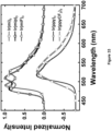
- the Ir(ppy) 3 and Ir(ppyCF 3 ) 3 complexes emit in the green, with the CF 3 substituents leading to a small blue shift in emission.
- the complexes have photoluminescence lifetimes ( ⁇ ) in the microsecond range at both room temperature and 77K, and high quantum yields ( ⁇ PL > 90%) (see Tables 1, 4, and 5 for the full photophysical characterization of the compounds).
- ⁇ and ⁇ PL observed are comparable to those found in other homoleptic tris-cyclometalated iridium (III) complexes ( J. Y. Zhuang, et al., New J. Chem. 2015, 39, 246 ; M. E.
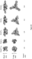
- the Ir(ppy) 3 complex has a slightly ellipsoidal shape (aspect ratio of 1.2) due to a compression along the C 3 axis.
- the Ir(mi) 3 complex has a more oblate spheroidal shape, with an aspect ratio of 2.2. Extending the imidazolyl ligand by appending an additional phenyl group in Ir(mip) 3 increases the aspect ratio to 3.0. Addition of CF 3 groups decreases the aspect ratio relative to the parent complexes, giving ratios for Ir(miF) 3 of 1.9, and Ir(ppyCF 3 ) 3 of 1.0. In all cases, the long axis of the oblate shape lies perpendicular to the C 3 axis.
- the molecular orientation of the luminescent complex relative to the substrate can be established from the optical anisotropy of dopant-based films ( vide infra ) .
- the dopant's TDM needs to be mapped onto the molecular frame of the compound.
- This mapping of the TDM of the triplet excited state for each dopant was carried out using time-dependent density functional theory (TDDFT) with the zero-order regular approximation (ZORA) that incorporates spin-orbit coupling ( E. van Lenthe, et al., The Journal of Chemical Physics 1994, 101, 9783 ; E. vanLenthe, et al., J. Chem. Phys. 1996, 105, 6505 ; E. v.
- the TDM is localized in the plane of a single Ir(C ⁇ N) moiety with the origin on the Ir atom ( Figure 29 ).
- the C 3 axis of the Ir(C ⁇ N) 3 complex leads to three such TDMs in the molecule whose orientations lie at the angle, ⁇ , relative to the Ir-N bond. Mapping the orientation of the TDM onto the full molecular frame gives its angle, ⁇ , with the C 3 axis.
- a horizontal TDM alignment is indicative a dopant oriented with the C 3 axis perpendicular to the substrate.
- ⁇ 90°
- ⁇ changes no more than 0.01 for a decrease in ⁇ from 90° to 84°. This is within the error range of APDS measurement (0.01-0.04), indicating directions of TDMs in all compounds are close to be in ideal condition.
- the anisotropy data for Ir(mip) 3 doped films supports the hypothesis that maximizing the ⁇ - ⁇ interaction area of the dopant and organic surface, and thus the van der Waals attractive forces, drives horizontal alignment.
- Molecular interactions between Ir(mip) 3 and the host during deposition is expected to be strongest when the long axis of the oblate spheroid is parallel to the substrate.
- the Coulomb force exerted by the permanent dipole moment is roughly equal when the PDM is pointed either at or away from the substrate. Since their modeling predicted a significantly lower magnitude for Coulomb relative to the van der Waals interactions, the Coulomb term only becomes relevant for dopants having a small aspect ratio, especially when deposited in host materials with high PDMs (the host molecules used in the Kim study has a PDM of 5.0 D, Table 3) ( C. K. Moon, et al., Nature Communications 2017, 8 ). The energetic models thus suggest that Coulomb forces acting on molecules with high dipole moments should favor dopant alignment.
- the net horizontal alignment of Ir(ppyCF 3 ) 3 compared to Ir(ppy) 3 is attributed to the CF 3 groups, suggesting that chemical asymmetry can increase the degree of horizontal alignment of the TDMs in the thin film.
- FIG. 30 A plot of the anisotropy factor versus the aspect ratio of the compounds studied here, as well as the cyano-substituted derivatives of Kim, et al., is shown in Figure 30 .
- the compounds are clustered into three groups depending the type (or absence) of substituent, with each grouping having a similar dependence of ⁇ on the aspect ratio.
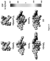
- the presence of chemical asymmetry can be illustrated using the electrostatic surface potential of the complex.
- the ESP calculated for the unsubstituted complexes is relatively uniform, whereas in both the CF 3 - and cyano-substituted derivatives, the ESPs are non-uniform ( Figure 31 ).
- the color of the ESP surface is based on the energy of a proton moved across the surface.
- a large negative energy (red) denotes a high negative charge at the surface, whereas a large positive energy (blue) indicates a high positive charge at the surface of the molecule.
- the most negative ESPs of the acceptor substituted molecules are symmetrically disposed around the C 3 axis, forming a "patch" of high ESP.
- the patch of high ESP reinforces an alignment of the molecule that favors low ⁇ .
- Dopant alignment appears to be a cooperative process, with both high aspect ratio and non-uniform ESP contributing to a lower ⁇ .
- the cyano substituents promote a higher degree of dopant alignment than CF 3 -substitution for a given dopant aspect ratio.
- FIGs 32 to 35 illustrate the device along with the performance data obtained using the structure: glass substrate / 70 nm ITO / 50 nm 4,4'-cyclohexylidenebis [N,N-bis(4-methylphenyl)benzenamine] (TAPC) / 15 nm EML / 50 nm 3,3',5,5'-tetra[(m-pyridyl)-phen-3-yl]biphenyl (BP4mPy) / 1.5 nm 8-hydroxyquinolinato lithium (LiQ) / 100 nm Al ( Figure 32 ).
- TAPC 4,4'-cyclohexylidenebis [N,N-bis(4-methylphenyl)benzenamine]
- BP4mPy 4,4'-cyclohexylidenebis [N,N-bis(4-methylphenyl)benzenamine]
- BP4mPy 4,4'-cyclohexylidenebis [N,N-
- the mixed host system was employed to enhance injection and transport of charges in the emissive layer, resulting in improved charge balance in the EML and low drive voltage ( K. Udagawa, et al., Adv. Opt. Mater. 2016, 4, 86 ).
- the device performance parameters are summarized in Table 7. Table 7.
- the electroluminescence (EL) spectra have distinct vibronic features and no detectable host emission, consistent with efficient exciton trapping on the dopant.
- the modal power distributions of the PHOLEDs were calculated based on Green's function analysis, using the ⁇ values determined by ADPS and FPIM ( R. R. Chance, et al., Opt. Express 2007, 15, 1762 ).
- This analysis permits estimation of the fraction of the EL emission in the forward direction (air mode) versus waveguided modes in the OLED and in the glass substrate, and surface plasmon modes in the cathode.
- outcoupling efficiencies (air mode) are consistent with the degree of dopant alignment from the ADPS and FPIM measurements: outcoupling is highest for Ir(mip) 3 with 32.8% of the light forward scattered, compared to 24.6 % for Ir(ppy) 3 .
- V T voltage at 0.1 cd/m 2
- V T of OLEDs using Ir(miF) 3 and Ir(ppyCF 3 ) 3 are 3.9 V and 4.5V, respectively ( Figure 34 ).
- the larger V T for the devices with CF 3 substituted dopants is attributed to a large interfacial dipole from spontaneous ordering of dopant PDMs at the EML/ETL interface ( Y. Noguchi, et al., Appl. Phys. Lett. 2013, 102 ; K. Osada, et al., Org. Electron. 2018, 58, 313 ).
- the PDMs estimated from DFT calculations for the non-fluorinated dopants are 6.4-6.9 D, whereas those of the CF 3 substituted derivatives are 12.7 and 16.3 D for Ir(miF) 3 and Ir(ppyCF 3 ) 3 , respectively (Table 4).
- the PDM coincides with the C 3 axis of the molecule ( Figure 21 ).
- the increase in V T suggests that Ir(miF) 3 and Ir(ppyCF 3 ) 3 are aligned with the CF 3 groups oriented toward the vacuum interface during the deposition. This ordering polarizes the HTL/EML interface to hinder injection of holes into the EML, which shifts the J-V curve to higher voltages, as observed.
- This work provides two approaches to achieve net alignment of tris -cyclometalated Ir complexes in vacuum deposited films. Altering the molecular shape to approximate an oblate spheroid or adding functional groups to one face of the molecule can lead to a net horizontal alignment of the transition dipole moments in doped films. While the oblate shape may drive the complex toward a parallel arrangement relative to the substrate, the principal axis of the molecule can be directed either toward or away from the substrate. The addition of trifluoromethyl substituents to one face of the molecule will not only promote net alignment relative to the substrate but can also orient of the principal axis of the complex to be directed either toward or away from the substrate, depending on the site of substitution. Moreover, these two effects, when acting in concert, can lead to further improvement in the degree of horizontal alignment, and hence lead to a higher outcoupling efficiency when used in OLEDs.
Landscapes
- Chemical & Material Sciences (AREA)
- Organic Chemistry (AREA)
- Engineering & Computer Science (AREA)
- Materials Engineering (AREA)
- Crystallography & Structural Chemistry (AREA)
- Inorganic Chemistry (AREA)
- Physics & Mathematics (AREA)
- Optics & Photonics (AREA)
- Electroluminescent Light Sources (AREA)
Claims (11)
- Composé électroluminescent ayant une zone superficielle à potentiel électrostatique fortement négatif,dans lequel le composé comporte un ligand LA représenté par la structure suivante :
 dans laquelle le ligand LA est coordonné à un métal M tel que représenté par les traits pointillés et le métal M est facultativement coordonné à un ou plusieurs ligand LB.
 - Composé selon la revendication 1, dans lequel le composé a la formule M(LA)x(LB)y, dans laquelle :M est un métal choisi parmi le groupe constitué de Re, Os, Rh, Ir, Pd, Pt, Ag, Ag et Cu,LB est un ligand monoanionique bidentate,x vaut 1, 2 ou 3,y vaut 0, 1 ou 2, etx + y est l'état d'oxydation du métal.
- Composé selon la revendication 1, dans lequel le composé ayant la formule Ir(LA)3 est l'isomère facial.
- Composé selon la revendication 1, dans lequel le composé a une charge neutre.
- Dispositif électroluminescent organique (OLED) comportant :une anode,une cathode, etune couche organique disposée entre l'anode et la cathode, la couche organique comportant un composé électroluminescent selon l'une quelconque des revendications précédentes.
- OLED selon la revendication 5, dans lequel la couche organique est une couche émissive, et le composé est un dopant émissif ou un dopant non émissif.
- OLED selon la revendication 5, dans lequel la couche organique comporte en outre un hôte, dans lequel l'hôte comporte au moins un groupe chimique choisi parmi le groupe constitué d'un triphénylène, d'un carbazole, d'un dibenzothiophène, d'un dibenzofurane, d'un dibenzosélénophène, d'un azatriphénylène, d'un azacarbazole, d'un aza-dibenzothiophène, d'un aza-dibenzofurane et d'un aza-dibenzosélénophène.
- OLED selon la revendication 5, dans lequel l'hôte est choisi parmi le groupe constitué de


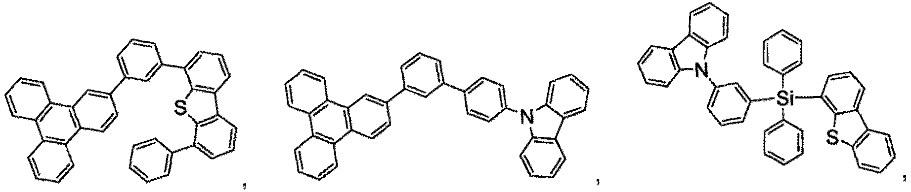

- Produit de consommation comportant un dispositif électroluminescent organique (OLED) comportant :une anode,une cathode, etune couche organique disposée entre l'anode et la cathode, la couche organique comportant un composé électroluminescent selon l'une quelconque des revendications 1 à 4.
- Produit de consommation selon la revendication 9, dans lequel le produit de consommation est choisi parmi le groupe constitué d'un écran plat, d'un moniteur informatique, d'un moniteur médical, d'un téléviseur, d'un panneau d'affichage, d'une lumière pour une signalisation et/ou un éclairage intérieur ou extérieur, d'un affichage tête haute, d'un écran entièrement ou partiellement transparent, d'un écran souple, d'une imprimante laser, d'un téléphone, d'un téléphone cellulaire, d'une tablette, d'un téléphone-tablette, d'un assistant numérique personnel (PDA), d'un dispositif portable, d'un ordinateur portable, d'un appareil de prise de vues numérique, d'un caméscope, d'un viseur, d'un micro-écran, d'un affichage en 3D, d'un affichage de réalité virtuelle ou de réalité augmentée, d'un véhicule, d'un mur de grande surface, d'un écran de salle de spectacle ou de stade, d'un dispositif de luminothérapie et d'une enseigne.
- Formulation comportant un composé selon la revendication 1.
Priority Applications (1)
| Application Number | Priority Date | Filing Date | Title |
|---|---|---|---|
| EP24205549.9A EP4471041A3 (fr) | 2021-06-08 | 2022-06-07 | Alignement moléculaire de luminophores homoleptiques à base d'iridium |
Applications Claiming Priority (2)
| Application Number | Priority Date | Filing Date | Title |
|---|---|---|---|
| US202163208106P | 2021-06-08 | 2021-06-08 | |
| US17/830,751 US20230133787A1 (en) | 2021-06-08 | 2022-06-02 | Molecular Alignment of Homoleptic Iridium Phosphors |
Related Child Applications (1)
| Application Number | Title | Priority Date | Filing Date |
|---|---|---|---|
| EP24205549.9A Division EP4471041A3 (fr) | 2021-06-08 | 2022-06-07 | Alignement moléculaire de luminophores homoleptiques à base d'iridium |
Publications (3)
| Publication Number | Publication Date |
|---|---|
| EP4112701A2 EP4112701A2 (fr) | 2023-01-04 |
| EP4112701A3 EP4112701A3 (fr) | 2023-04-26 |
| EP4112701B1 true EP4112701B1 (fr) | 2024-10-16 |
Family
ID=81975334
Family Applications (2)
| Application Number | Title | Priority Date | Filing Date |
|---|---|---|---|
| EP24205549.9A Pending EP4471041A3 (fr) | 2021-06-08 | 2022-06-07 | Alignement moléculaire de luminophores homoleptiques à base d'iridium |
| EP22177684.2A Active EP4112701B1 (fr) | 2021-06-08 | 2022-06-07 | Alignement moléculaire de phosphores homoleptiques d'iridium |
Family Applications Before (1)
| Application Number | Title | Priority Date | Filing Date |
|---|---|---|---|
| EP24205549.9A Pending EP4471041A3 (fr) | 2021-06-08 | 2022-06-07 | Alignement moléculaire de luminophores homoleptiques à base d'iridium |
Country Status (4)
| Country | Link |
|---|---|
| US (1) | US20230133787A1 (fr) |
| EP (2) | EP4471041A3 (fr) |
| KR (1) | KR20220165665A (fr) |
| CN (1) | CN115448956A (fr) |
Families Citing this family (2)
| Publication number | Priority date | Publication date | Assignee | Title |
|---|---|---|---|---|
| US12339330B2 (en) * | 2022-03-01 | 2025-06-24 | Government Of The United States Of America, As Represented By The Secretary Of Commerce | Thin film magnetic field magnitude sensor |
| US12339331B2 (en) * | 2022-03-01 | 2025-06-24 | Guvernment Of The United States Of America, As Represented By The Secretary Of Commerce | Thin film magnetic field vector sensor |
Family Cites Families (326)
| Publication number | Priority date | Publication date | Assignee | Title |
|---|---|---|---|---|
| GB191200102A (en) | 1912-01-01 | 1912-07-18 | Coventry Chain Company Ltd | Improvements in Driving Chains. |
| GB191502007A (en) | 1915-02-08 | 1915-08-12 | Eles Linsey Heninger | Egg Crate. |
| US4769292A (en) | 1987-03-02 | 1988-09-06 | Eastman Kodak Company | Electroluminescent device with modified thin film luminescent zone |
| GB8909011D0 (en) | 1989-04-20 | 1989-06-07 | Friend Richard H | Electroluminescent devices |
| US5061569A (en) | 1990-07-26 | 1991-10-29 | Eastman Kodak Company | Electroluminescent device with organic electroluminescent medium |
| JPH0773529A (ja) | 1993-08-31 | 1995-03-17 | Hitachi Ltd | 光磁気記録方式および光磁気記録媒体 |
| DE69412567T2 (de) | 1993-11-01 | 1999-02-04 | Hodogaya Chemical Co., Ltd., Tokio/Tokyo | Aminverbindung und sie enthaltende Elektrolumineszenzvorrichtung |
| US5707745A (en) | 1994-12-13 | 1998-01-13 | The Trustees Of Princeton University | Multicolor organic light emitting devices |
| US5703436A (en) | 1994-12-13 | 1997-12-30 | The Trustees Of Princeton University | Transparent contacts for organic devices |
| KR0117693Y1 (ko) | 1995-03-16 | 1998-04-23 | 천일선 | 곡물볶음기의 도어개폐장치 |
| US6939625B2 (en) | 1996-06-25 | 2005-09-06 | Nôrthwestern University | Organic light-emitting diodes and methods for assembly and enhanced charge injection |
| US5844363A (en) | 1997-01-23 | 1998-12-01 | The Trustees Of Princeton Univ. | Vacuum deposited, non-polymeric flexible organic light emitting devices |
| US6013982A (en) | 1996-12-23 | 2000-01-11 | The Trustees Of Princeton University | Multicolor display devices |
| US6091195A (en) | 1997-02-03 | 2000-07-18 | The Trustees Of Princeton University | Displays having mesa pixel configuration |
| US5834893A (en) | 1996-12-23 | 1998-11-10 | The Trustees Of Princeton University | High efficiency organic light emitting devices with light directing structures |
| EP0879868B1 (fr) | 1997-05-19 | 2002-04-03 | Canon Kabushiki Kaisha | Composé organique et dispositif électroluminescent l'utilisant |
| US6413656B1 (en) | 1998-09-14 | 2002-07-02 | The University Of Southern California | Reduced symmetry porphyrin molecules for producing enhanced luminosity from phosphorescent organic light emitting devices |
| US6303238B1 (en) | 1997-12-01 | 2001-10-16 | The Trustees Of Princeton University | OLEDs doped with phosphorescent compounds |
| US6337102B1 (en) | 1997-11-17 | 2002-01-08 | The Trustees Of Princeton University | Low pressure vapor phase deposition of organic thin films |
| US6087196A (en) | 1998-01-30 | 2000-07-11 | The Trustees Of Princeton University | Fabrication of organic semiconductor devices using ink jet printing |
| US6097147A (en) | 1998-09-14 | 2000-08-01 | The Trustees Of Princeton University | Structure for high efficiency electroluminescent device |
| US6830828B2 (en) | 1998-09-14 | 2004-12-14 | The Trustees Of Princeton University | Organometallic complexes as phosphorescent emitters in organic LEDs |
| US6461747B1 (en) | 1999-07-22 | 2002-10-08 | Fuji Photo Co., Ltd. | Heterocyclic compounds, materials for light emitting devices and light emitting devices using the same |
| US6294398B1 (en) | 1999-11-23 | 2001-09-25 | The Trustees Of Princeton University | Method for patterning devices |
| US6458475B1 (en) | 1999-11-24 | 2002-10-01 | The Trustee Of Princeton University | Organic light emitting diode having a blue phosphorescent molecule as an emitter |
| US6821645B2 (en) | 1999-12-27 | 2004-11-23 | Fuji Photo Film Co., Ltd. | Light-emitting material comprising orthometalated iridium complex, light-emitting device, high efficiency red light-emitting device, and novel iridium complex |
| KR100377321B1 (ko) | 1999-12-31 | 2003-03-26 | 주식회사 엘지화학 | 피-형 반도체 성질을 갖는 유기 화합물을 포함하는 전기소자 |
| US6670645B2 (en) | 2000-06-30 | 2003-12-30 | E. I. Du Pont De Nemours And Company | Electroluminescent iridium compounds with fluorinated phenylpyridines, phenylpyrimidines, and phenylquinolines and devices made with such compounds |
| JP5241053B2 (ja) | 2000-08-11 | 2013-07-17 | ザ、トラスティーズ オブ プリンストン ユニバーシティ | 有機金属化合物及び放射移行有機電気燐光体 |
| AU2002222565A1 (en) * | 2000-11-30 | 2002-06-11 | Canon Kabushiki Kaisha | Luminescent element and display |
| CN1285601C (zh) | 2000-11-30 | 2006-11-22 | 佳能株式会社 | 发光器件和显示器 |
| JP4154145B2 (ja) | 2000-12-01 | 2008-09-24 | キヤノン株式会社 | 金属配位化合物、発光素子及び表示装置 |
| US6579630B2 (en) | 2000-12-07 | 2003-06-17 | Canon Kabushiki Kaisha | Deuterated semiconducting organic compounds used for opto-electronic devices |
| JP4438042B2 (ja) | 2001-03-08 | 2010-03-24 | キヤノン株式会社 | 金属配位化合物、電界発光素子及び表示装置 |
| JP4307000B2 (ja) | 2001-03-08 | 2009-08-05 | キヤノン株式会社 | 金属配位化合物、電界発光素子及び表示装置 |
| JP4307001B2 (ja) | 2001-03-14 | 2009-08-05 | キヤノン株式会社 | 金属配位化合物、電界発光素子及び表示装置 |
| DE10116962A1 (de) | 2001-04-05 | 2002-10-10 | Covion Organic Semiconductors | Rhodium- und Iridium-Komplexe |
| US7071615B2 (en) | 2001-08-20 | 2006-07-04 | Universal Display Corporation | Transparent electrodes |
| US7431968B1 (en) | 2001-09-04 | 2008-10-07 | The Trustees Of Princeton University | Process and apparatus for organic vapor jet deposition |
| US6835469B2 (en) | 2001-10-17 | 2004-12-28 | The University Of Southern California | Phosphorescent compounds and devices comprising the same |
| US7166368B2 (en) | 2001-11-07 | 2007-01-23 | E. I. Du Pont De Nemours And Company | Electroluminescent platinum compounds and devices made with such compounds |
| US6863997B2 (en) | 2001-12-28 | 2005-03-08 | The Trustees Of Princeton University | White light emitting OLEDs from combined monomer and aggregate emission |
| KR100691543B1 (ko) | 2002-01-18 | 2007-03-09 | 주식회사 엘지화학 | 새로운 전자 수송용 물질 및 이를 이용한 유기 발광 소자 |
| US6653654B1 (en) | 2002-05-01 | 2003-11-25 | The University Of Hong Kong | Electroluminescent materials |
| JP4106974B2 (ja) | 2002-06-17 | 2008-06-25 | コニカミノルタホールディングス株式会社 | 有機エレクトロルミネッセンス素子及び表示装置 |
| US20030230980A1 (en) | 2002-06-18 | 2003-12-18 | Forrest Stephen R | Very low voltage, high efficiency phosphorescent oled in a p-i-n structure |
| US6916554B2 (en) | 2002-11-06 | 2005-07-12 | The University Of Southern California | Organic light emitting materials and devices |
| US7189989B2 (en) | 2002-08-22 | 2007-03-13 | Fuji Photo Film Co., Ltd. | Light emitting element |
| DE10238903A1 (de) | 2002-08-24 | 2004-03-04 | Covion Organic Semiconductors Gmbh | Rhodium- und Iridium-Komplexe |
| CN100439469C (zh) | 2002-08-27 | 2008-12-03 | 富士胶片株式会社 | 有机金属配位化合物、有机el元件及有机el显示器 |
| JP4261855B2 (ja) | 2002-09-19 | 2009-04-30 | キヤノン株式会社 | フェナントロリン化合物及びそれを用いた有機発光素子 |
| US6687266B1 (en) | 2002-11-08 | 2004-02-03 | Universal Display Corporation | Organic light emitting materials and devices |
| DE10310887A1 (de) | 2003-03-11 | 2004-09-30 | Covion Organic Semiconductors Gmbh | Matallkomplexe |
| EP1717291A3 (fr) | 2003-04-15 | 2007-03-21 | Merck Patent GmbH | Mélanges de semi-conducteurs organiques aptes à l'émission et de matières matricielles, leur utilisation et composants électroniques contenant ces mélanges |
| CN102516312A (zh) | 2003-07-22 | 2012-06-27 | 出光兴产株式会社 | 金属络合化合物和使用了该化合物的有机电致发光元件 |
| JP4561221B2 (ja) | 2003-07-31 | 2010-10-13 | 三菱化学株式会社 | 化合物、電荷輸送材料および有機電界発光素子 |
| TWI390006B (zh) | 2003-08-07 | 2013-03-21 | Nippon Steel Chemical Co | Organic EL materials with aluminum clamps |
| DE10338550A1 (de) | 2003-08-19 | 2005-03-31 | Basf Ag | Übergangsmetallkomplexe mit Carbenliganden als Emitter für organische Licht-emittierende Dioden (OLEDs) |
| US7504049B2 (en) | 2003-08-25 | 2009-03-17 | Semiconductor Energy Laboratory Co., Ltd. | Electrode device for organic device, electronic device having electrode device for organic device, and method of forming electrode device for organic device |
| HU0302888D0 (en) | 2003-09-09 | 2003-11-28 | Pribenszky Csaba Dr | In creasing of efficacity of stable storage by freezing of embryos in preimplantation stage with pretreatment by pressure |
| DE10345572A1 (de) | 2003-09-29 | 2005-05-19 | Covion Organic Semiconductors Gmbh | Metallkomplexe |
| JP5112601B2 (ja) | 2003-10-07 | 2013-01-09 | 三井化学株式会社 | 複素環化合物および該化合物を含有する有機電界発光素子 |
| EP1683804B1 (fr) | 2003-11-04 | 2013-07-31 | Takasago International Corporation | Complexe de platine et element luminescent |
| JP4215621B2 (ja) | 2003-11-17 | 2009-01-28 | 富士電機アセッツマネジメント株式会社 | 回路遮断器の外部操作ハンドル装置 |
| TWI245068B (en) * | 2003-11-18 | 2005-12-11 | Chi Mei Optoelectronics Corp | Iridium complex as light emitting material and organic light emitting diode device |
| DE10357044A1 (de) | 2003-12-04 | 2005-07-14 | Novaled Gmbh | Verfahren zur Dotierung von organischen Halbleitern mit Chinondiiminderivaten |
| US7029766B2 (en) | 2003-12-05 | 2006-04-18 | Eastman Kodak Company | Organic element for electroluminescent devices |
| US20050123791A1 (en) | 2003-12-05 | 2005-06-09 | Deaton Joseph C. | Organic electroluminescent devices |
| US7332232B2 (en) | 2004-02-03 | 2008-02-19 | Universal Display Corporation | OLEDs utilizing multidentate ligand systems |
| TW200535134A (en) | 2004-02-09 | 2005-11-01 | Nippon Steel Chemical Co | Aminodibenzodioxin derivative and organic electroluminescent device using same |
| KR100834327B1 (ko) | 2004-03-11 | 2008-06-02 | 미쓰비시 가가꾸 가부시키가이샤 | 전하 수송막용 조성물 및 이온 화합물, 이를 이용한 전하수송막 및 유기 전계 발광 장치, 및 유기 전계 발광 장치의제조 방법 및 전하 수송막의 제조 방법 |
| TW200531592A (en) | 2004-03-15 | 2005-09-16 | Nippon Steel Chemical Co | Organic electroluminescent device |
| JP4869565B2 (ja) | 2004-04-23 | 2012-02-08 | 富士フイルム株式会社 | 有機電界発光素子 |
| US7154114B2 (en) | 2004-05-18 | 2006-12-26 | Universal Display Corporation | Cyclometallated iridium carbene complexes for use as hosts |
| US7279704B2 (en) | 2004-05-18 | 2007-10-09 | The University Of Southern California | Complexes with tridentate ligands |
| US7534505B2 (en) | 2004-05-18 | 2009-05-19 | The University Of Southern California | Organometallic compounds for use in electroluminescent devices |
| US20060008670A1 (en) | 2004-07-06 | 2006-01-12 | Chun Lin | Organic light emitting materials and devices |
| US20060182993A1 (en) | 2004-08-10 | 2006-08-17 | Mitsubishi Chemical Corporation | Compositions for organic electroluminescent device and organic electroluminescent device |
| US7402345B2 (en) * | 2004-09-14 | 2008-07-22 | E.I. Du Pont De Nemours And Company | Electroluminescent iridium compounds with fluorinated phenylpyridine ligands, and devices made with such compounds |
| KR100880220B1 (ko) | 2004-10-04 | 2009-01-28 | 엘지디스플레이 주식회사 | 유기 실리콘을 갖는 페닐 피리딘기를 포함하는 이리듐화합물계 발광 화합물 및 이를 발색 재료로서 사용하는유기전계발광소자 |
| DE102004057072A1 (de) | 2004-11-25 | 2006-06-01 | Basf Ag | Verwendung von Übergangsmetall-Carbenkomplexen in organischen Licht-emittierenden Dioden (OLEDs) |
| US8021765B2 (en) | 2004-11-29 | 2011-09-20 | Samsung Mobile Display Co., Ltd. | Phenylcarbazole-based compound and organic electroluminescent device employing the same |
| JP4478555B2 (ja) | 2004-11-30 | 2010-06-09 | キヤノン株式会社 | 金属錯体、発光素子及び画像表示装置 |
| US20060134459A1 (en) | 2004-12-17 | 2006-06-22 | Shouquan Huo | OLEDs with mixed-ligand cyclometallated complexes |
| TWI242596B (en) | 2004-12-22 | 2005-11-01 | Ind Tech Res Inst | Organometallic compound and organic electroluminescent device including the same |
| CA2589711A1 (fr) | 2004-12-23 | 2006-06-29 | Ciba Specialty Chemicals Holding Inc. | Complexes metalliques electroluminescents a ligands carbene nucleophiles |
| JP2008526766A (ja) | 2004-12-30 | 2008-07-24 | イー・アイ・デュポン・ドウ・ヌムール・アンド・カンパニー | 有機金属錯体 |
| US20070181874A1 (en) | 2004-12-30 | 2007-08-09 | Shiva Prakash | Charge transport layers and organic electron devices comprising same |
| KR101239462B1 (ko) | 2005-01-05 | 2013-03-06 | 이데미쓰 고산 가부시키가이샤 | 방향족 아민 유도체 및 이를 이용한 유기 전기발광 소자 |
| KR20070100965A (ko) | 2005-02-03 | 2007-10-15 | 메르크 파텐트 게엠베하 | 금속 착물 |
| WO2006081780A1 (fr) | 2005-02-04 | 2006-08-10 | Novaled Ag | Dopants pour semi-conducteurs organiques |
| KR100676965B1 (ko) | 2005-03-05 | 2007-02-02 | 주식회사 두산 | 신규 이리듐 착화합물 및 이를 이용한 유기 전계 발광 소자 |
| KR100797469B1 (ko) | 2005-03-08 | 2008-01-24 | 엘지전자 주식회사 | 적색 인광 화합물 및 이를 사용한 유기전계발광소자 |
| KR100803125B1 (ko) | 2005-03-08 | 2008-02-14 | 엘지전자 주식회사 | 적색 인광 화합물 및 이를 사용한 유기전계발광소자 |
| CN101180262B (zh) | 2005-04-18 | 2012-06-13 | 出光兴产株式会社 | 芳香族三胺化合物以及应用该化合物的有机电致发光元件 |
| WO2006114966A1 (fr) | 2005-04-18 | 2006-11-02 | Konica Minolta Holdings, Inc. | Dispositif électroluminescent organique, affichage et dispositif d'illumination |
| US7807275B2 (en) | 2005-04-21 | 2010-10-05 | Universal Display Corporation | Non-blocked phosphorescent OLEDs |
| CN1321125C (zh) | 2005-04-30 | 2007-06-13 | 中国科学院长春应用化学研究所 | 喹啉类氮杂环为配体的红光铱配合物及其应用 |
| US7902374B2 (en) | 2005-05-06 | 2011-03-08 | Universal Display Corporation | Stability OLED materials and devices |
| US8586204B2 (en) | 2007-12-28 | 2013-11-19 | Universal Display Corporation | Phosphorescent emitters and host materials with improved stability |
| US8007927B2 (en) | 2007-12-28 | 2011-08-30 | Universal Display Corporation | Dibenzothiophene-containing materials in phosphorescent light emitting diodes |
| US9051344B2 (en) | 2005-05-06 | 2015-06-09 | Universal Display Corporation | Stability OLED materials and devices |
| EP2277978B1 (fr) | 2005-05-31 | 2016-03-30 | Universal Display Corporation | Hotes de triphenylene dans des diodes luminescentes phosphorescentes |
| JPWO2007007463A1 (ja) | 2005-07-11 | 2009-01-29 | 出光興産株式会社 | 電子吸引性置換基を有する含窒素複素環誘導体及びそれを用いた有機エレクトロルミネッセンス素子 |
| US8187727B2 (en) | 2005-07-22 | 2012-05-29 | Lg Chem, Ltd. | Imidazole derivatives, preparation method thereof and organic electronic device using the same |
| JP5317386B2 (ja) | 2005-08-05 | 2013-10-16 | 出光興産株式会社 | 含窒素複素環誘導体及びそれを用いた有機エレクトロルミネッセンス素子 |
| WO2007018067A1 (fr) | 2005-08-05 | 2007-02-15 | Idemitsu Kosan Co., Ltd. | Composé complexe de métaux de transition et dispositif électroluminescent organique l’utilisant |
| JP4848152B2 (ja) | 2005-08-08 | 2011-12-28 | 出光興産株式会社 | 芳香族アミン誘導体及びそれを用いた有機エレクトロルミネッセンス素子 |
| JP5040216B2 (ja) | 2005-08-30 | 2012-10-03 | 三菱化学株式会社 | 有機化合物、電荷輸送材料、有機電界発光素子用材料、電荷輸送材料組成物及び有機電界発光素子 |
| US9023489B2 (en) | 2005-11-07 | 2015-05-05 | Lg Display Co., Ltd. | Red phosphorescent compounds and organic electroluminescent devices using the same |
| KR100662378B1 (ko) | 2005-11-07 | 2007-01-02 | 엘지전자 주식회사 | 적색 인광 화합물 및 이를 사용한 유기전계발광소자 |
| US20070104977A1 (en) | 2005-11-07 | 2007-05-10 | Idemitsu Kosan Co., Ltd. | Organic electroluminescent device |
| US7462406B2 (en) | 2005-11-15 | 2008-12-09 | Eastman Kodak Company | OLED devices with dinuclear copper compounds |
| US20070145888A1 (en) | 2005-11-16 | 2007-06-28 | Idemitsu Kosan Co., Ltd. | Aromatic amine derivatives and organic electroluminescence device using the same |
| US20080233410A1 (en) | 2005-11-17 | 2008-09-25 | Idemitsu Kosan Co., Ltd. | Transition metal complex compound |
| EP1956022B1 (fr) | 2005-12-01 | 2012-07-25 | Nippon Steel Chemical Co., Ltd. | Compose pour element electroluminescent organique et element electroluminescent organique |
| US7999103B2 (en) | 2005-12-15 | 2011-08-16 | Chuo University | Metal complex compound and organic electroluminescence device using the compound |
| WO2007080801A1 (fr) | 2006-01-11 | 2007-07-19 | Idemitsu Kosan Co., Ltd. | Nouveau derive imide, materiau pour element electroluminescent organique et element electroluminescent organique le comprenant |
| US7759489B2 (en) | 2006-01-27 | 2010-07-20 | Idemitsu Kosan Co., Ltd. | Transition metal complex compound and organic electroluminescence device using the compound |
| KR102103062B1 (ko) | 2006-02-10 | 2020-04-22 | 유니버셜 디스플레이 코포레이션 | 시클로금속화 이미다조[1,2-f]페난트리딘 및 디이미다조[1,2-a:1',2'-c]퀴나졸린 리간드, 및 이의 등전자성 및 벤즈고리화된 유사체의 금속 착체 |
| WO2007108362A1 (fr) | 2006-03-17 | 2007-09-27 | Konica Minolta Holdings, Inc. | Dispositif électroluminescent organique, dispositif d'éclairage et d'affichage |
| JP4823730B2 (ja) | 2006-03-20 | 2011-11-24 | 新日鐵化学株式会社 | 発光層化合物及び有機電界発光素子 |
| EP1837926B1 (fr) | 2006-03-21 | 2008-05-07 | Novaled AG | Radicaux ou diradicaux hétérocycliques, leur dimères, oligomères, polymères, composés spiro et polycycliques. Leur usage dans des semi-conducteurs organiques et dispositifs électroniques. |
| KR20070097139A (ko) | 2006-03-23 | 2007-10-04 | 엘지전자 주식회사 | 적색 인광 화합물 및 이를 사용한 유기전계발광소자 |
| JPWO2007111263A1 (ja) | 2006-03-27 | 2009-08-13 | 出光興産株式会社 | 含窒素複素環誘導体及びそれを用いた有機エレクトロルミネッセンス素子 |
| JP5273910B2 (ja) | 2006-03-31 | 2013-08-28 | キヤノン株式会社 | 発光素子用有機化合物、発光素子および画像表示装置 |
| CN101460514A (zh) | 2006-04-04 | 2009-06-17 | 巴斯夫欧洲公司 | 含有一个非碳烯配体和一个或两个碳烯配体的过渡金属配合物及它们在oled中的用途 |
| ATE550342T1 (de) | 2006-04-05 | 2012-04-15 | Basf Se | Heteroleptische übergangsmetall-carben-komplexe und deren verwendung in organischen leuchtdioden (oleds) |
| US20090128024A1 (en) | 2006-04-20 | 2009-05-21 | Kenichi Fukuoka | Organic light-emitting device |
| EP2639231B1 (fr) | 2006-04-26 | 2019-02-06 | Idemitsu Kosan Co., Ltd. | Dérivé d'amine aromatique et élément électroluminescent organique l'utilisant |
| JP5432523B2 (ja) | 2006-05-11 | 2014-03-05 | 出光興産株式会社 | 有機エレクトロルミネッセンス素子 |
| US20070278936A1 (en) | 2006-06-02 | 2007-12-06 | Norman Herron | Red emitter complexes of IR(III) and devices made with such compounds |
| EP2034538B1 (fr) | 2006-06-02 | 2013-10-09 | Idemitsu Kosan Co., Ltd. | Matériau pour élément organique électroluminescent et élément organique électroluminescent utilisant le matériau |
| TW200815446A (en) | 2006-06-05 | 2008-04-01 | Idemitsu Kosan Co | Organic electroluminescent device and material for organic electroluminescent device |
| US7675228B2 (en) | 2006-06-14 | 2010-03-09 | E.I. Du Pont De Nemours And Company | Electroluminescent iridium compounds with silylated, germanylated, and stannylated ligands, and devices made with such compounds |
| US7629158B2 (en) | 2006-06-16 | 2009-12-08 | The Procter & Gamble Company | Cleaning and/or treatment compositions |
| CN101473464B (zh) | 2006-06-22 | 2014-04-23 | 出光兴产株式会社 | 应用含有杂环的芳胺衍生物的有机电致发光元件 |
| JP2008021687A (ja) | 2006-07-10 | 2008-01-31 | Mitsubishi Chemicals Corp | 有機電界発光素子用材料、有機電界発光素子用組成物及び有機電界発光素子 |
| US7736756B2 (en) | 2006-07-18 | 2010-06-15 | Global Oled Technology Llc | Light emitting device containing phosphorescent complex |
| KR20090040895A (ko) | 2006-08-23 | 2009-04-27 | 이데미쓰 고산 가부시키가이샤 | 방향족 아민 유도체 및 이들을 이용한 유기 전기발광 소자 |
| JP2008069120A (ja) | 2006-09-15 | 2008-03-27 | Idemitsu Kosan Co Ltd | 芳香族アミン誘導体及びそれらを用いた有機エレクトロルミネッセンス素子 |
| JP5556014B2 (ja) | 2006-09-20 | 2014-07-23 | コニカミノルタ株式会社 | 有機エレクトロルミネッセンス素子 |
| US7968146B2 (en) | 2006-11-01 | 2011-06-28 | The Trustees Of Princeton University | Hybrid layers for use in coatings on electronic devices or other articles |
| EP2080762B1 (fr) | 2006-11-09 | 2016-09-14 | Nippon Steel & Sumikin Chemical Co., Ltd. | Composé pour un dispositif électroluminescent organique et dispositif électroluminescent organique |
| JP5133259B2 (ja) | 2006-11-24 | 2013-01-30 | 出光興産株式会社 | 芳香族アミン誘導体及びそれを用いた有機エレクトロルミネッセンス素子 |
| US8119255B2 (en) | 2006-12-08 | 2012-02-21 | Universal Display Corporation | Cross-linkable iridium complexes and organic light-emitting devices using the same |
| JP5493357B2 (ja) | 2006-12-13 | 2014-05-14 | コニカミノルタ株式会社 | 有機エレクトロルミネッセンス素子、表示装置及び照明装置 |
| JP2008150310A (ja) | 2006-12-15 | 2008-07-03 | Idemitsu Kosan Co Ltd | 芳香族アミン誘導体及びそれらを用いた有機エレクトロルミネッセンス素子 |
| JP5262104B2 (ja) | 2006-12-27 | 2013-08-14 | 住友化学株式会社 | 金属錯体、高分子化合物及びこれらを含む素子 |
| WO2008096609A1 (fr) | 2007-02-05 | 2008-08-14 | Idemitsu Kosan Co., Ltd. | Composé complexe en métal de transition et dispositif électroluminescent organique l'utilisant |
| DE602008004738D1 (de) | 2007-02-23 | 2011-03-10 | Basf Se | Elektrolumineszente metallkomplexe mit benzotriazolen |
| CN101657518A (zh) | 2007-03-08 | 2010-02-24 | 通用显示公司 | 磷光材料 |
| US9130177B2 (en) | 2011-01-13 | 2015-09-08 | Universal Display Corporation | 5-substituted 2 phenylquinoline complexes materials for light emitting diode |
| JP5053713B2 (ja) | 2007-05-30 | 2012-10-17 | キヤノン株式会社 | リン光発光材料、それを用いた有機電界発光素子及び画像表示装置 |
| WO2008156879A1 (fr) | 2007-06-20 | 2008-12-24 | Universal Display Corporation | Matériaux à base d'imidazophénantridine phosphorescente bleue |
| CN101720330B (zh) | 2007-06-22 | 2017-06-09 | Udc爱尔兰有限责任公司 | 发光Cu(I)络合物 |
| DE102007031220B4 (de) | 2007-07-04 | 2022-04-28 | Novaled Gmbh | Chinoide Verbindungen und deren Verwendung in halbleitenden Matrixmaterialien, elektronischen und optoelektronischen Bauelementen |
| KR101577465B1 (ko) | 2007-07-05 | 2015-12-14 | 바스프 에스이 | 카르벤 전이 금속 착체 이미터, 및 디실릴카르바졸, 디실릴디벤조푸란, 디실릴디벤조티오펜, 디실릴디벤조포스폴, 디실릴디벤조티오펜 s-옥사이드 및 디실릴디벤조티오펜 s,s-디옥사이드로부터 선택된 1종 이상의 화합물을 포함하는 유기 발광 다이오드 |
| DE102007031261A1 (de) * | 2007-07-05 | 2009-01-08 | Universtität Regensburg | Lumineszierende Metallkomplexe mit sperrigen Hilfsliganden |
| WO2009008099A1 (fr) | 2007-07-10 | 2009-01-15 | Idemitsu Kosan Co., Ltd. | Matériau pour élément à électroluminescence organique, et élément à électroluminescence organique préparé à l'aide du matériau |
| US8080658B2 (en) | 2007-07-10 | 2011-12-20 | Idemitsu Kosan Co., Ltd. | Material for organic electroluminescent element and organic electroluminescent element employing the same |
| US8372527B2 (en) | 2007-07-11 | 2013-02-12 | Idemitsu Kosan Co., Ltd. | Material for organic electroluminescent element, and organic electroluminescent element |
| WO2009011327A1 (fr) | 2007-07-18 | 2009-01-22 | Idemitsu Kosan Co., Ltd. | Matériau de dispositif électroluminescent organique et dispositif électroluminescent organique |
| WO2009020095A1 (fr) | 2007-08-06 | 2009-02-12 | Idemitsu Kosan Co., Ltd. | Dérivé d'amine aromatique et dispositif électroluminescent organique utilisant celui-ci |
| CN101827834B (zh) | 2007-08-08 | 2015-11-25 | 通用显示公司 | 含苯并[9,10]菲的苯并稠合的噻吩或苯并稠合的呋喃化合物 |
| JP2009040728A (ja) | 2007-08-09 | 2009-02-26 | Canon Inc | 有機金属錯体及びこれを用いた有機発光素子 |
| US8956737B2 (en) | 2007-09-27 | 2015-02-17 | Lg Display Co., Ltd. | Red phosphorescent compound and organic electroluminescent device using the same |
| US8067100B2 (en) | 2007-10-04 | 2011-11-29 | Universal Display Corporation | Complexes with tridentate ligands |
| US8258297B2 (en) | 2007-10-17 | 2012-09-04 | Basf Se | Transition metal complexes with bridged carbene ligands and use thereof in OLEDs |
| KR100950968B1 (ko) | 2007-10-18 | 2010-04-02 | 에스에프씨 주식회사 | 적색 인광 화합물 및 이를 이용한 유기전계발광소자 |
| US20090101870A1 (en) | 2007-10-22 | 2009-04-23 | E. I. Du Pont De Nemours And Company | Electron transport bi-layers and devices made with such bi-layers |
| US7914908B2 (en) | 2007-11-02 | 2011-03-29 | Global Oled Technology Llc | Organic electroluminescent device having an azatriphenylene derivative |
| EP2216313B1 (fr) | 2007-11-15 | 2013-02-20 | Idemitsu Kosan Co., Ltd. | Dérivé de benzochrysène et dispositif électroluminescent organique l'utilisant |
| KR100933226B1 (ko) | 2007-11-20 | 2009-12-22 | 다우어드밴스드디스플레이머티리얼 유한회사 | 신규한 적색 인광 화합물 및 이를 발광재료로서 채용하고있는 유기발광소자 |
| JP5390396B2 (ja) | 2007-11-22 | 2014-01-15 | 出光興産株式会社 | 有機el素子および有機el材料含有溶液 |
| WO2009066779A1 (fr) | 2007-11-22 | 2009-05-28 | Idemitsu Kosan Co., Ltd. | Élément el organique |
| WO2009073245A1 (fr) | 2007-12-06 | 2009-06-11 | Universal Display Corporation | Complexes organométalliques électroluminescents |
| US8221905B2 (en) | 2007-12-28 | 2012-07-17 | Universal Display Corporation | Carbazole-containing materials in phosphorescent light emitting diodes |
| KR20100097180A (ko) | 2007-12-28 | 2010-09-02 | 이데미쓰 고산 가부시키가이샤 | 방향족 아민 유도체 및 그들을 이용한 유기 전기발광 소자 |
| US8471248B2 (en) | 2008-02-12 | 2013-06-25 | Basf Se | Electroluminiscent metal complexes with dibenzo[f,h] quinoxalines |
| KR101379133B1 (ko) | 2008-05-29 | 2014-03-28 | 이데미쓰 고산 가부시키가이샤 | 방향족 아민 유도체 및 그들을 사용한 유기 전기발광 소자 |
| KR101011857B1 (ko) | 2008-06-04 | 2011-02-01 | 주식회사 두산 | 벤조플루오란센 유도체 및 이를 이용한 유기 발광 소자 |
| US8057919B2 (en) | 2008-06-05 | 2011-11-15 | Idemitsu Kosan Co., Ltd. | Material for organic electroluminescence device and organic electroluminescence device using the same |
| US8049411B2 (en) | 2008-06-05 | 2011-11-01 | Idemitsu Kosan Co., Ltd. | Material for organic electroluminescence device and organic electroluminescence device using the same |
| US8318323B2 (en) | 2008-06-05 | 2012-11-27 | Idemitsu Kosan Co., Ltd. | Polycyclic compounds and organic electroluminescence device employing the same |
| KR20160126093A (ko) | 2008-06-10 | 2016-11-01 | 유디씨 아일랜드 리미티드 | 중수소화된 전이 금속 착물 및 이의 유기 발광 다이오드에서의 용도 ⅴ |
| CN102131891B (zh) | 2008-06-30 | 2014-01-29 | 通用显示公司 | 具有含硫基团的空穴传输材料 |
| KR101176261B1 (ko) | 2008-09-02 | 2012-08-22 | 주식회사 두산 | 안트라센 유도체 및 이를 이용한 유기 전계 발광 소자 |
| WO2010027583A1 (fr) | 2008-09-03 | 2010-03-11 | Universal Display Corporation | Matières phosphorescentes |
| TWI555734B (zh) | 2008-09-16 | 2016-11-01 | 環球展覽公司 | 磷光物質 |
| KR101044843B1 (ko) | 2008-09-24 | 2011-06-28 | 주식회사 엘지화학 | 신규한 안트라센 유도체 및 이를 이용한 유기전자소자 |
| US8101755B2 (en) | 2008-10-23 | 2012-01-24 | Semiconductor Energy Laboratory Co., Ltd. | Organometallic complex including pyrazine derivative |
| KR101348699B1 (ko) | 2008-10-29 | 2014-01-08 | 엘지디스플레이 주식회사 | 적색 인광 물질 및 이를 이용한 유기전계발광소자 |
| KR100901888B1 (ko) | 2008-11-13 | 2009-06-09 | (주)그라쎌 | 신규한 전기발광용 유기금속 화합물 및 이를 발광재료로 채용하고 있는 전기발광소자 |
| DE102008057051B4 (de) | 2008-11-13 | 2021-06-17 | Merck Patent Gmbh | Materialien für organische Elektrolumineszenzvorrichtungen |
| DE102008057050B4 (de) | 2008-11-13 | 2021-06-02 | Merck Patent Gmbh | Materialien für organische Elektrolumineszenzvorrichtungen |
| KR101600127B1 (ko) | 2008-11-25 | 2016-03-04 | 이데미쓰 고산 가부시키가이샤 | 방향족 아민 유도체 및 유기 전기발광 소자 |
| US8815415B2 (en) | 2008-12-12 | 2014-08-26 | Universal Display Corporation | Blue emitter with high efficiency based on imidazo[1,2-f] phenanthridine iridium complexes |
| JP2010138121A (ja) | 2008-12-12 | 2010-06-24 | Canon Inc | トリアジン化合物及びこれを用いた有機発光素子 |
| DE102008064200A1 (de) | 2008-12-22 | 2010-07-01 | Merck Patent Gmbh | Organische Elektrolumineszenzvorrichtung |
| KR20100079458A (ko) | 2008-12-31 | 2010-07-08 | 덕산하이메탈(주) | 비스-카바졸 화합물 및 이를 이용한 유기전기소자, 그 단말 |
| US9067947B2 (en) | 2009-01-16 | 2015-06-30 | Universal Display Corporation | Organic electroluminescent materials and devices |
| DE102009007038A1 (de) | 2009-02-02 | 2010-08-05 | Merck Patent Gmbh | Metallkomplexe |
| US8759818B2 (en) | 2009-02-27 | 2014-06-24 | E I Du Pont De Nemours And Company | Deuterated compounds for electronic applications |
| KR101511072B1 (ko) | 2009-03-20 | 2015-04-10 | 롬엔드하스전자재료코리아유한회사 | 신규한 유기 발광 화합물 및 이를 포함하는 유기 전계 발광소자 |
| US8722205B2 (en) | 2009-03-23 | 2014-05-13 | Universal Display Corporation | Heteroleptic iridium complex |
| TWI751419B (zh) | 2009-04-06 | 2022-01-01 | 美商環球展覽公司 | 包含新穎配位體結構之金屬錯合物 |
| TWI687408B (zh) | 2009-04-28 | 2020-03-11 | 美商環球展覽公司 | 具有甲基-d3取代之銥錯合物 |
| US8603642B2 (en) | 2009-05-13 | 2013-12-10 | Global Oled Technology Llc | Internal connector for organic electronic devices |
| US8586203B2 (en) | 2009-05-20 | 2013-11-19 | Universal Display Corporation | Metal complexes with boron-nitrogen heterocycle containing ligands |
| JP2011018765A (ja) | 2009-07-08 | 2011-01-27 | Furukawa Electric Co Ltd:The | 光増幅用光ファイバおよび光ファイバ増幅器ならびに光ファイバレーザ |
| JP4590020B1 (ja) | 2009-07-31 | 2010-12-01 | 富士フイルム株式会社 | 電荷輸送材料及び有機電界発光素子 |
| WO2011021689A1 (fr) | 2009-08-21 | 2011-02-24 | 東ソー株式会社 | Dérivés dazine cycliques, procédés pour produire ceux-ci, et élément électroluminescent organique contenant ceux-ci en tant que composant |
| DE102009049587A1 (de) | 2009-10-16 | 2011-04-21 | Merck Patent Gmbh | Metallkomplexe |
| US9306175B2 (en) | 2009-10-23 | 2016-04-05 | Hodogaya Chemical Co., Ltd. | Organic electroluminescent device |
| EP2493906B1 (fr) | 2009-10-28 | 2015-10-21 | Basf Se | Composees coordinatives heteroleptiques du type carben et leur usage dans electronique organique |
| KR101288566B1 (ko) | 2009-12-16 | 2013-07-22 | 제일모직주식회사 | 유기광전소자용 화합물 및 이를 포함하는 유기광전소자 |
| EP2513187A2 (fr) | 2009-12-18 | 2012-10-24 | Plextronics, Inc. | Copolymères de 3,4-dialcoxythiophènes et procédés de fabrication et dispositifs |
| KR101183722B1 (ko) | 2009-12-30 | 2012-09-17 | 주식회사 두산 | 트리페닐렌계 화합물 및 이를 포함하는 유기 전계 발광 소자 |
| KR101290011B1 (ko) | 2009-12-30 | 2013-07-30 | 주식회사 두산 | 유기발광 화합물 및 이를 포함한 유기 전계 발광 소자 |
| JP4617393B1 (ja) | 2010-01-15 | 2011-01-26 | 富士フイルム株式会社 | 有機電界発光素子 |
| CN102712612A (zh) | 2010-01-21 | 2012-10-03 | 出光兴产株式会社 | 芳香族胺衍生物和使用其的有机电致发光元件 |
| KR20110088898A (ko) | 2010-01-29 | 2011-08-04 | 주식회사 이엘엠 | 유기 전기 발광 조성물 및 이를 포함하는 유기 전기 발광 소자 |
| US20120319098A1 (en) | 2010-02-25 | 2012-12-20 | Shinshu University | Substituted pyridyl compound and organic electroluminescent element |
| US9156870B2 (en) | 2010-02-25 | 2015-10-13 | Universal Display Corporation | Phosphorescent emitters |
| DE102010002482B3 (de) | 2010-03-01 | 2012-01-05 | Technische Universität Braunschweig | Lumineszente Organometallverbindung |
| US9175211B2 (en) | 2010-03-03 | 2015-11-03 | Universal Display Corporation | Phosphorescent materials |
| KR101182444B1 (ko) | 2010-04-01 | 2012-09-12 | 삼성디스플레이 주식회사 | 유기 발광 소자 |
| WO2012020327A1 (fr) | 2010-04-16 | 2012-02-16 | Basf Se | Complexes benzimidazole-carbène pontés et leur utilisation dans les delo |
| TWI395804B (zh) | 2010-05-18 | 2013-05-11 | Ind Tech Res Inst | 有機金屬化合物及包含其之有機電激發光裝置及組合物 |
| JP2012006878A (ja) * | 2010-06-25 | 2012-01-12 | Mitsubishi Chemicals Corp | 有機金属錯体、発光材料、有機電界発光素子材料、有機金属錯体含有組成物、有機電界発光素子、有機elディスプレイおよび有機el照明 |
| EP2595208A1 (fr) | 2010-07-13 | 2013-05-22 | Toray Industries, Inc. | Elément électroluminescent |
| KR20120032054A (ko) | 2010-07-28 | 2012-04-05 | 롬엔드하스전자재료코리아유한회사 | 신규한 유기 발광 화합물 및 이를 포함하는 유기 전계 발광 소자 |
| JP5825846B2 (ja) | 2010-09-13 | 2015-12-02 | キヤノン株式会社 | 新規縮合多環化合物およびそれを有する有機発光素子 |
| JP5707818B2 (ja) | 2010-09-28 | 2015-04-30 | コニカミノルタ株式会社 | 有機エレクトロルミネッセンス素子用材料、有機エレクトロルミネッセンス素子、表示素子、照明装置及び金属錯体化合物 |
| JP5656534B2 (ja) | 2010-09-29 | 2015-01-21 | キヤノン株式会社 | インドロ[3,2,1−jk]カルバゾール化合物及びこれを有する有機発光素子 |
| US9349964B2 (en) | 2010-12-24 | 2016-05-24 | Lg Chem, Ltd. | Organic light emitting diode and manufacturing method thereof |
| KR101350581B1 (ko) | 2010-12-29 | 2014-01-16 | 주식회사 엘지화학 | 새로운 화합물 및 이를 이용한 유기 발광 소자 |
| US8415031B2 (en) | 2011-01-24 | 2013-04-09 | Universal Display Corporation | Electron transporting compounds |
| JP6042352B2 (ja) | 2011-02-23 | 2016-12-14 | ユニバーサル ディスプレイ コーポレイション | 新規四座配位白金錯体 |
| WO2012128298A1 (fr) | 2011-03-24 | 2012-09-27 | 出光興産株式会社 | Dérivé de bis-carbazole et élément électroluminescent organique l'utilisant |
| JP5906114B2 (ja) | 2011-03-31 | 2016-04-20 | ユー・ディー・シー アイルランド リミテッド | 電荷輸送材料、有機電界発光素子、発光装置、表示装置および照明装置 |
| JP5984450B2 (ja) | 2011-03-31 | 2016-09-06 | ユー・ディー・シー アイルランド リミテッド | 有機電界発光素子、並びに、該素子を用いた発光装置、表示装置、照明装置及び該素子用の化合物 |
| KR101298735B1 (ko) | 2011-04-06 | 2013-08-21 | 한국화학연구원 | 신규 유기금속 화합물 및 이를 이용한 유기 발광 소자 |
| US8795850B2 (en) | 2011-05-19 | 2014-08-05 | Universal Display Corporation | Phosphorescent heteroleptic phenylbenzimidazole dopants and new synthetic methodology |
| KR20120129733A (ko) | 2011-05-20 | 2012-11-28 | (주)씨에스엘쏠라 | 유기발광화합물 및 이를 이용한 유기 광소자 |
| US10103340B2 (en) | 2011-06-03 | 2018-10-16 | Merck Patent Gmbh | Metal complexes |
| WO2012177006A2 (fr) | 2011-06-22 | 2012-12-27 | 덕산하이메탈(주) | Composé destiné à des éléments électroniques organiques, éléments électroniques organiques utilisant ce composé, et dispositif électronique pour ce composé |
| US9309223B2 (en) | 2011-07-08 | 2016-04-12 | Semiconductor Energy Laboratory Co., Ltd. | Heterocyclic compound, light-emitting element, light-emitting device, electronic device, and lighting device |
| JP5882621B2 (ja) | 2011-08-01 | 2016-03-09 | キヤノン株式会社 | アミノインドロ[3,2,1−jk]カルバゾール化合物及びそれを有する有機発光素子 |
| TWI429652B (zh) | 2011-08-05 | 2014-03-11 | Ind Tech Res Inst | 有機金屬化合物及包含其之有機電激發光裝置 |
| JP6129075B2 (ja) | 2011-08-18 | 2017-05-17 | 出光興産株式会社 | ビスカルバゾール誘導体およびこれを用いた有機エレクトロルミネッセンス素子 |
| WO2013036043A2 (fr) | 2011-09-09 | 2013-03-14 | 주식회사 엘지화학 | Matériau pour dispositif électroluminescent organique et dispositif électroluminescent organique employant ce matériau |
| KR102048688B1 (ko) | 2011-09-09 | 2019-11-26 | 이데미쓰 고산 가부시키가이샤 | 질소 함유 헤테로 방향족환 화합물 |
| WO2013038843A1 (fr) | 2011-09-12 | 2013-03-21 | 新日鉄住金化学株式会社 | Élément électroluminescent organique |
| US9634255B2 (en) | 2011-09-15 | 2017-04-25 | Idemitsu Kosan Co., Ltd. | Aromatic amine derivative and organic electroluminescence element using same |
| KR20140075011A (ko) * | 2011-10-19 | 2014-06-18 | 이 아이 듀폰 디 네모아 앤드 캄파니 | 조명용 유기 전자 소자 |
| KR101897044B1 (ko) | 2011-10-20 | 2018-10-23 | 에스에프씨 주식회사 | 유기금속 화합물 및 이를 포함하는 유기전계발광소자 |
| KR20130053846A (ko) | 2011-11-16 | 2013-05-24 | 롬엔드하스전자재료코리아유한회사 | 신규한 유기 발광 화합물 및 이를 채용하고 있는 유기 전계 발광 소자 |
| JP5783007B2 (ja) | 2011-11-21 | 2015-09-24 | コニカミノルタ株式会社 | 有機エレクトロルミネッセンス素子および照明装置 |
| WO2013081315A1 (fr) | 2011-11-28 | 2013-06-06 | 덕산하이메탈(주) | Composé pour un dispositif électronique organique, dispositif électronique organique comprenant celui-ci et dispositif électronique comprenant le dispositif électronique organique |
| JP6170501B2 (ja) | 2011-11-30 | 2017-07-26 | ノヴァレッド ゲーエムベーハー | ディスプレイ |
| CN103959503B (zh) | 2011-12-05 | 2016-08-24 | 出光兴产株式会社 | 有机电致发光元件用材料以及有机电致发光元件 |
| US9512355B2 (en) | 2011-12-09 | 2016-12-06 | Universal Display Corporation | Organic light emitting materials |
| KR101921896B1 (ko) | 2011-12-12 | 2018-11-26 | 메르크 파텐트 게엠베하 | 전자 소자용 화합물 |
| TWI490211B (zh) | 2011-12-23 | 2015-07-01 | Semiconductor Energy Lab | 有機金屬錯合物,發光元件,發光裝置,電子裝置及照明裝置 |
| KR101497135B1 (ko) | 2011-12-29 | 2015-03-02 | 제일모직 주식회사 | 유기광전자소자용 화합물, 이를 포함하는 유기발광소자 및 상기 유기발광소자를 포함하는 표시장치 |
| CN107814821B (zh) | 2012-01-12 | 2025-03-07 | Udc爱尔兰有限责任公司 | 具有二苯并[f,h]喹喔啉的金属配合物 |
| CN106986858B (zh) | 2012-01-16 | 2019-08-27 | 默克专利有限公司 | 有机金属络合物 |
| US10211413B2 (en) | 2012-01-17 | 2019-02-19 | Universal Display Corporation | Organic electroluminescent materials and devices |
| JP5981770B2 (ja) | 2012-01-23 | 2016-08-31 | ユー・ディー・シー アイルランド リミテッド | 有機電界発光素子、有機電界発光素子用電荷輸送材料、並びに、該素子を用いた発光装置、表示装置及び照明装置 |
| WO2013118812A1 (fr) | 2012-02-10 | 2013-08-15 | 出光興産株式会社 | Élément électroluminescent organique |
| WO2013120577A1 (fr) | 2012-02-14 | 2013-08-22 | Merck Patent Gmbh | Composés de spirobifluorène pour dispositifs organiques électroluminescents |
| US9054323B2 (en) | 2012-03-15 | 2015-06-09 | Universal Display Corporation | Secondary hole transporting layer with diarylamino-phenyl-carbazole compounds |
| DE102012005215B3 (de) | 2012-03-15 | 2013-04-11 | Novaled Ag | Aromatische Amin-Terphenyl-Verbindungen und Verwendung derselben in organischen halbleitenden Bauelementen |
| US20130248830A1 (en) | 2012-03-22 | 2013-09-26 | Rohm And Haas Electronic Materials Korea Ltd. | Charge transport layers and films containing the same |
| WO2013145667A1 (fr) | 2012-03-29 | 2013-10-03 | ソニー株式会社 | Élément électroluminescent organique |
| DE102012205945A1 (de) | 2012-04-12 | 2013-10-17 | Siemens Aktiengesellschaft | Organische Superdonoren mit mindestens zwei gekoppelten Carben-Gruppen und deren Verwendung als n-Dotierstoffe |
| KR101565200B1 (ko) | 2012-04-12 | 2015-11-02 | 주식회사 엘지화학 | 신규한 화합물 및 이를 이용한 유기 발광 소자 |
| JP2015155378A (ja) | 2012-04-18 | 2015-08-27 | 保土谷化学工業株式会社 | トリフェニレン環構造を有する化合物および有機エレクトロルミネッセンス素子 |
| WO2013175747A1 (fr) | 2012-05-22 | 2013-11-28 | 出光興産株式会社 | Élément électroluminescent organique |
| JP5182441B1 (ja) * | 2012-05-24 | 2013-04-17 | 三菱化学株式会社 | 有機電界発光素子、有機電界発光照明装置及び有機電界発光表示装置 |
| WO2013174471A1 (fr) | 2012-05-24 | 2013-11-28 | Merck Patent Gmbh | Complexes de métaux comprenant des cycles hétéroaromatiques condensés |
| WO2013180376A1 (fr) | 2012-05-30 | 2013-12-05 | Alpha Chem Co., Ltd. | Nouveau matériau de transport d'électrons et dispositif organique électroluminescent l'utilisant |
| DE102012209523A1 (de) | 2012-06-06 | 2013-12-12 | Osram Opto Semiconductors Gmbh | Hauptgruppenmetallkomplexe als p-Dotanden für organische elektronische Matrixmaterialien |
| CN102702075A (zh) | 2012-06-13 | 2012-10-03 | 吉林奥来德光电材料股份有限公司 | 含有三芳胺结构的有机电致发光材料及制备方法和应用 |
| CN103508940B (zh) | 2012-06-21 | 2017-05-03 | 昆山维信诺显示技术有限公司 | 一种6,6‑双取代‑6‑H‑苯并[cd]芘衍生物、中间体及制备方法和应用 |
| KR101507423B1 (ko) | 2012-06-22 | 2015-04-08 | 덕산네오룩스 주식회사 | 화합물, 이를 이용한 유기전기소자 및 그 전자 장치 |
| JP6088161B2 (ja) | 2012-06-29 | 2017-03-01 | 出光興産株式会社 | 芳香族アミン誘導体及び有機エレクトロルミネッセンス素子 |
| KR101344787B1 (ko) | 2012-07-04 | 2013-12-26 | 제일모직주식회사 | 유기광전자소자용 화합물, 이를 포함하는 유기발광소자 및 상기 유기발광소자를 포함하는 표시장치 |
| EP2684932B8 (fr) | 2012-07-09 | 2016-12-21 | Hodogaya Chemical Co., Ltd. | Matériau de matrice dopé avec une composé mesomeric radialène |
| KR20140008126A (ko) | 2012-07-10 | 2014-01-21 | 삼성디스플레이 주식회사 | 유기 발광 장치 |
| US9559310B2 (en) | 2012-07-11 | 2017-01-31 | Samsung Display Co., Ltd. | Compound with electron injection and/or electron transport capabilities and organic light-emitting device including the same |
| US9837622B2 (en) | 2012-07-13 | 2017-12-05 | Merck Patent Gmbh | Metal complexes |
| KR101452577B1 (ko) | 2012-07-20 | 2014-10-21 | 주식회사 두산 | 유기 발광 화합물 및 이를 이용한 유기 전계 발광 소자 |
| KR102155492B1 (ko) | 2012-07-23 | 2020-09-14 | 메르크 파텐트 게엠베하 | 플루오렌 및 이를 함유하는 전자 소자 |
| KR102583348B1 (ko) | 2012-07-23 | 2023-09-26 | 메르크 파텐트 게엠베하 | 화합물 및 유기 전계 발광 디바이스 |
| WO2014023377A2 (fr) | 2012-08-07 | 2014-02-13 | Merck Patent Gmbh | Complexes métalliques |
| EP2882766B1 (fr) | 2012-08-09 | 2019-11-27 | UDC Ireland Limited | Complexes de métaux de transition avec des ligands de type carbène et leur utilisation dans les oled |
| KR101497138B1 (ko) | 2012-08-21 | 2015-02-27 | 제일모직 주식회사 | 유기광전자소자 및 이를 포함하는 표시장치 |
| KR102128702B1 (ko) | 2012-08-21 | 2020-07-02 | 롬엔드하스전자재료코리아유한회사 | 신규한 유기 전계 발광 화합물 및 이를 포함하는 유기 전계 발광 소자 |
| US9711741B2 (en) | 2012-08-24 | 2017-07-18 | Arizona Board Of Regents On Behalf Of Arizona State University | Metal compounds and methods and uses thereof |
| US20150228899A1 (en) | 2012-08-31 | 2015-08-13 | Idemitsu Kosan Co., Ltd. | Organic electroluminescent element |
| WO2014038456A1 (fr) | 2012-09-04 | 2014-03-13 | コニカミノルタ株式会社 | Élément électroluminescent organique, dispositif d'éclairage et dispositif d'affichage |
| KR101848885B1 (ko) | 2012-10-29 | 2018-04-16 | 삼성디스플레이 주식회사 | 아민계 화합물 및 이를 포함한 유기 발광 소자 |
| US8946697B1 (en) * | 2012-11-09 | 2015-02-03 | Universal Display Corporation | Iridium complexes with aza-benzo fused ligands |
| JP6253971B2 (ja) | 2012-12-28 | 2017-12-27 | 株式会社半導体エネルギー研究所 | 発光素子、発光装置、電子機器、及び照明装置 |
| KR101684979B1 (ko) | 2012-12-31 | 2016-12-09 | 제일모직 주식회사 | 유기광전자소자 및 이를 포함하는 표시장치 |
| WO2014104535A1 (fr) | 2012-12-31 | 2014-07-03 | 제일모직 주식회사 | Composé pour dispositif organique optoélectronique, diode organique électroluminescente le comprenant et appareil d'affichage comprenant ladite diode organique électroluminescente |
| KR20140087647A (ko) | 2012-12-31 | 2014-07-09 | 제일모직주식회사 | 유기광전자소자용 화합물, 이를 포함하는 유기발광소자 및 상기 유기발광소자를 포함하는 표시장치 |
| JP6071569B2 (ja) | 2013-01-17 | 2017-02-01 | キヤノン株式会社 | 有機発光素子 |
| US9627629B2 (en) | 2013-02-12 | 2017-04-18 | Samsung Electronics Co., Ltd. | Compound for organic optoelectronic device, organic light emitting diode including the same, and display including the organic light emitting diode |
| TWI612051B (zh) | 2013-03-01 | 2018-01-21 | 半導體能源研究所股份有限公司 | 有機金屬錯合物、發光元件、發光裝置、電子裝置、照明設備 |
| KR102081689B1 (ko) | 2013-03-15 | 2020-02-26 | 덕산네오룩스 주식회사 | 유기전기 소자용 화합물, 이를 이용한 유기전기소자 및 그 전자 장치 |
| US20140284580A1 (en) | 2013-03-22 | 2014-09-25 | E-Ray Optoelectronics Techonology Co., Ltd. | Electron transporting compounds and organic electroluminescent devices using the same |
| KR102399864B1 (ko) | 2013-03-26 | 2022-05-20 | 가부시키가이샤 한도오따이 에네루기 켄큐쇼 | 유기 화합물, 발광 소자, 발광 장치, 표시 장치, 전자 기기 및 조명 장치 |
| CN103694277A (zh) | 2013-12-12 | 2014-04-02 | 江西冠能光电材料有限公司 | 一种红色磷光有机发光二极管 |
| TWI666803B (zh) | 2014-09-17 | 2019-07-21 | 日商日鐵化學材料股份有限公司 | 有機電場發光元件及其製造方法 |
| US9397302B2 (en) * | 2014-10-08 | 2016-07-19 | Universal Display Corporation | Organic electroluminescent materials and devices |
| KR101818579B1 (ko) | 2014-12-09 | 2018-01-15 | 삼성에스디아이 주식회사 | 유기 광전자 소자 및 표시 장치 |
| KR101604647B1 (ko) | 2015-08-28 | 2016-03-21 | 덕산네오룩스 주식회사 | 유기전기 소자용 화합물, 이를 이용한 유기전기소자 및 그 전자 장치 |
| US11228003B2 (en) * | 2016-04-22 | 2022-01-18 | Universal Display Corporation | Organic electroluminescent materials and devices |
| TWI572601B (zh) * | 2016-06-07 | 2017-03-01 | 國立清華大學 | 鉑錯合物、有機發光二極體與可發出可見光或近紅外光的裝置 |
| CN106496278A (zh) * | 2016-09-02 | 2017-03-15 | 瑞声光电科技(常州)有限公司 | 铱配合物及其制备方法和应用铱配合物的电致发光器件 |
| CN106632499A (zh) * | 2016-12-09 | 2017-05-10 | 南京远淑医药科技有限公司 | 一种含铱配合物的深蓝色磷光材料与应用 |
| US10396298B2 (en) * | 2017-01-25 | 2019-08-27 | National Tsing Hua University | Iridium complex and organic light-emitting diode using the same |
-
2022
- 2022-06-02 US US17/830,751 patent/US20230133787A1/en active Pending
- 2022-06-07 EP EP24205549.9A patent/EP4471041A3/fr active Pending
- 2022-06-07 EP EP22177684.2A patent/EP4112701B1/fr active Active
- 2022-06-08 CN CN202210648105.2A patent/CN115448956A/zh active Pending
- 2022-06-08 KR KR1020220069495A patent/KR20220165665A/ko active Pending
Also Published As
| Publication number | Publication date |
|---|---|
| EP4471041A2 (fr) | 2024-12-04 |
| EP4112701A2 (fr) | 2023-01-04 |
| CN115448956A (zh) | 2022-12-09 |
| US20230133787A1 (en) | 2023-05-04 |
| EP4112701A3 (fr) | 2023-04-26 |
| KR20220165665A (ko) | 2022-12-15 |
| EP4471041A3 (fr) | 2025-05-28 |
Similar Documents
| Publication | Publication Date | Title |
|---|---|---|
| JP7541074B2 (ja) | 有機エレクトロルミネセンス材料及びデバイス | |
| JP7370400B2 (ja) | 有機エレクトロルミネセンス材料及びデバイス | |
| CN110265554B (zh) | 用于电致发光装置的主体材料 | |
| KR20230119621A (ko) | 유기 전계발광 물질 및 소자 | |
| KR20220122557A (ko) | 유기 전계발광 물질 및 디바이스 | |
| US12058929B2 (en) | Organic electroluminescent materials and devices | |
| EP4016659B1 (fr) | Matériaux et dispositifs électroluminescents organiques | |
| EP4075530B1 (fr) | Matériaux et dispositifs électroluminescents organiques | |
| EP4112701B1 (fr) | Alignement moléculaire de phosphores homoleptiques d'iridium | |
| KR20210059590A (ko) | 유기 전계발광 물질 및 디바이스 | |
| US20240292734A1 (en) | Organic electroluminescent device | |
| KR20230157266A (ko) | 유기 전계발광 물질 및 디바이스 | |
| KR102955605B1 (ko) | 유기 전계발광 물질 및 디바이스 | |
| CN113248531B (zh) | 有机电致发光材料和装置 | |
| KR20260056121A (ko) | 유기 전계발광 물질 및 디바이스 | |
| KR20240125470A (ko) | 유기 전계발광 물질 및 디바이스 | |
| KR20240167584A (ko) | 유기 전계발광 물질 및 디바이스 |
Legal Events
| Date | Code | Title | Description |
|---|---|---|---|
| PUAI | Public reference made under article 153(3) epc to a published international application that has entered the european phase |
Free format text: ORIGINAL CODE: 0009012 |
|
| STAA | Information on the status of an ep patent application or granted ep patent |
Free format text: STATUS: REQUEST FOR EXAMINATION WAS MADE |
|
| 17P | Request for examination filed |
Effective date: 20220607 |
|
| AK | Designated contracting states |
Kind code of ref document: A2 Designated state(s): AL AT BE BG CH CY CZ DE DK EE ES FI FR GB GR HR HU IE IS IT LI LT LU LV MC MK MT NL NO PL PT RO RS SE SI SK SM TR |
|
| PUAL | Search report despatched |
Free format text: ORIGINAL CODE: 0009013 |
|
| AK | Designated contracting states |
Kind code of ref document: A3 Designated state(s): AL AT BE BG CH CY CZ DE DK EE ES FI FR GB GR HR HU IE IS IT LI LT LU LV MC MK MT NL NO PL PT RO RS SE SI SK SM TR |
|
| RIC1 | Information provided on ipc code assigned before grant |
Ipc: C07F 15/00 20060101ALI20230323BHEP Ipc: C09K 11/06 20060101AFI20230323BHEP |
|
| GRAP | Despatch of communication of intention to grant a patent |
Free format text: ORIGINAL CODE: EPIDOSNIGR1 |
|
| STAA | Information on the status of an ep patent application or granted ep patent |
Free format text: STATUS: GRANT OF PATENT IS INTENDED |
|
| INTG | Intention to grant announced |
Effective date: 20240513 |
|
| GRAS | Grant fee paid |
Free format text: ORIGINAL CODE: EPIDOSNIGR3 |
|
| GRAA | (expected) grant |
Free format text: ORIGINAL CODE: 0009210 |
|
| STAA | Information on the status of an ep patent application or granted ep patent |
Free format text: STATUS: THE PATENT HAS BEEN GRANTED |
|
| AK | Designated contracting states |
Kind code of ref document: B1 Designated state(s): AL AT BE BG CH CY CZ DE DK EE ES FI FR GB GR HR HU IE IS IT LI LT LU LV MC MK MT NL NO PL PT RO RS SE SI SK SM TR |
|
| P01 | Opt-out of the competence of the unified patent court (upc) registered |
Free format text: CASE NUMBER: APP_51092/2024 Effective date: 20240910 |
|
| REG | Reference to a national code |
Ref country code: GB Ref legal event code: FG4D |
|
| REG | Reference to a national code |
Ref country code: CH Ref legal event code: EP Ref country code: DE Ref legal event code: R096 Ref document number: 602022006799 Country of ref document: DE |
|
| REG | Reference to a national code |
Ref country code: IE Ref legal event code: FG4D |
|
| REG | Reference to a national code |
Ref country code: LT Ref legal event code: MG9D |
|
| REG | Reference to a national code |
Ref country code: NL Ref legal event code: MP Effective date: 20241016 |
|
| REG | Reference to a national code |
Ref country code: AT Ref legal event code: MK05 Ref document number: 1732931 Country of ref document: AT Kind code of ref document: T Effective date: 20241016 |
|
| PG25 | Lapsed in a contracting state [announced via postgrant information from national office to epo] |
Ref country code: NL Free format text: LAPSE BECAUSE OF FAILURE TO SUBMIT A TRANSLATION OF THE DESCRIPTION OR TO PAY THE FEE WITHIN THE PRESCRIBED TIME-LIMIT Effective date: 20241016 |
|
| PG25 | Lapsed in a contracting state [announced via postgrant information from national office to epo] |
Ref country code: NL Free format text: LAPSE BECAUSE OF FAILURE TO SUBMIT A TRANSLATION OF THE DESCRIPTION OR TO PAY THE FEE WITHIN THE PRESCRIBED TIME-LIMIT Effective date: 20241016 |
|
| PG25 | Lapsed in a contracting state [announced via postgrant information from national office to epo] |
Ref country code: IS Free format text: LAPSE BECAUSE OF FAILURE TO SUBMIT A TRANSLATION OF THE DESCRIPTION OR TO PAY THE FEE WITHIN THE PRESCRIBED TIME-LIMIT Effective date: 20250216 Ref country code: HR Free format text: LAPSE BECAUSE OF FAILURE TO SUBMIT A TRANSLATION OF THE DESCRIPTION OR TO PAY THE FEE WITHIN THE PRESCRIBED TIME-LIMIT Effective date: 20241016 Ref country code: PT Free format text: LAPSE BECAUSE OF FAILURE TO SUBMIT A TRANSLATION OF THE DESCRIPTION OR TO PAY THE FEE WITHIN THE PRESCRIBED TIME-LIMIT Effective date: 20250217 |
|
| PG25 | Lapsed in a contracting state [announced via postgrant information from national office to epo] |
Ref country code: FI Free format text: LAPSE BECAUSE OF FAILURE TO SUBMIT A TRANSLATION OF THE DESCRIPTION OR TO PAY THE FEE WITHIN THE PRESCRIBED TIME-LIMIT Effective date: 20241016 |
|
| PG25 | Lapsed in a contracting state [announced via postgrant information from national office to epo] |
Ref country code: BG Free format text: LAPSE BECAUSE OF FAILURE TO SUBMIT A TRANSLATION OF THE DESCRIPTION OR TO PAY THE FEE WITHIN THE PRESCRIBED TIME-LIMIT Effective date: 20241016 |
|
| PG25 | Lapsed in a contracting state [announced via postgrant information from national office to epo] |
Ref country code: ES Free format text: LAPSE BECAUSE OF FAILURE TO SUBMIT A TRANSLATION OF THE DESCRIPTION OR TO PAY THE FEE WITHIN THE PRESCRIBED TIME-LIMIT Effective date: 20241016 |
|
| PG25 | Lapsed in a contracting state [announced via postgrant information from national office to epo] |
Ref country code: NO Free format text: LAPSE BECAUSE OF FAILURE TO SUBMIT A TRANSLATION OF THE DESCRIPTION OR TO PAY THE FEE WITHIN THE PRESCRIBED TIME-LIMIT Effective date: 20250116 |
|
| PG25 | Lapsed in a contracting state [announced via postgrant information from national office to epo] |
Ref country code: LV Free format text: LAPSE BECAUSE OF FAILURE TO SUBMIT A TRANSLATION OF THE DESCRIPTION OR TO PAY THE FEE WITHIN THE PRESCRIBED TIME-LIMIT Effective date: 20241016 Ref country code: GR Free format text: LAPSE BECAUSE OF FAILURE TO SUBMIT A TRANSLATION OF THE DESCRIPTION OR TO PAY THE FEE WITHIN THE PRESCRIBED TIME-LIMIT Effective date: 20250117 Ref country code: AT Free format text: LAPSE BECAUSE OF FAILURE TO SUBMIT A TRANSLATION OF THE DESCRIPTION OR TO PAY THE FEE WITHIN THE PRESCRIBED TIME-LIMIT Effective date: 20241016 |
|
| PG25 | Lapsed in a contracting state [announced via postgrant information from national office to epo] |
Ref country code: PL Free format text: LAPSE BECAUSE OF FAILURE TO SUBMIT A TRANSLATION OF THE DESCRIPTION OR TO PAY THE FEE WITHIN THE PRESCRIBED TIME-LIMIT Effective date: 20241016 |
|
| PG25 | Lapsed in a contracting state [announced via postgrant information from national office to epo] |
Ref country code: RS Free format text: LAPSE BECAUSE OF FAILURE TO SUBMIT A TRANSLATION OF THE DESCRIPTION OR TO PAY THE FEE WITHIN THE PRESCRIBED TIME-LIMIT Effective date: 20250116 |
|
| PG25 | Lapsed in a contracting state [announced via postgrant information from national office to epo] |
Ref country code: SM Free format text: LAPSE BECAUSE OF FAILURE TO SUBMIT A TRANSLATION OF THE DESCRIPTION OR TO PAY THE FEE WITHIN THE PRESCRIBED TIME-LIMIT Effective date: 20241016 |
|
| PGFP | Annual fee paid to national office [announced via postgrant information from national office to epo] |
Ref country code: DE Payment date: 20250618 Year of fee payment: 4 |
|
| PG25 | Lapsed in a contracting state [announced via postgrant information from national office to epo] |
Ref country code: DK Free format text: LAPSE BECAUSE OF FAILURE TO SUBMIT A TRANSLATION OF THE DESCRIPTION OR TO PAY THE FEE WITHIN THE PRESCRIBED TIME-LIMIT Effective date: 20241016 |
|
| REG | Reference to a national code |
Ref country code: DE Ref legal event code: R097 Ref document number: 602022006799 Country of ref document: DE |
|
| PG25 | Lapsed in a contracting state [announced via postgrant information from national office to epo] |
Ref country code: EE Free format text: LAPSE BECAUSE OF FAILURE TO SUBMIT A TRANSLATION OF THE DESCRIPTION OR TO PAY THE FEE WITHIN THE PRESCRIBED TIME-LIMIT Effective date: 20241016 |
|
| PG25 | Lapsed in a contracting state [announced via postgrant information from national office to epo] |
Ref country code: RO Free format text: LAPSE BECAUSE OF FAILURE TO SUBMIT A TRANSLATION OF THE DESCRIPTION OR TO PAY THE FEE WITHIN THE PRESCRIBED TIME-LIMIT Effective date: 20241016 |
|
| PG25 | Lapsed in a contracting state [announced via postgrant information from national office to epo] |
Ref country code: SK Free format text: LAPSE BECAUSE OF FAILURE TO SUBMIT A TRANSLATION OF THE DESCRIPTION OR TO PAY THE FEE WITHIN THE PRESCRIBED TIME-LIMIT Effective date: 20241016 |
|
| PG25 | Lapsed in a contracting state [announced via postgrant information from national office to epo] |
Ref country code: CZ Free format text: LAPSE BECAUSE OF FAILURE TO SUBMIT A TRANSLATION OF THE DESCRIPTION OR TO PAY THE FEE WITHIN THE PRESCRIBED TIME-LIMIT Effective date: 20241016 |
|
| PG25 | Lapsed in a contracting state [announced via postgrant information from national office to epo] |
Ref country code: IT Free format text: LAPSE BECAUSE OF FAILURE TO SUBMIT A TRANSLATION OF THE DESCRIPTION OR TO PAY THE FEE WITHIN THE PRESCRIBED TIME-LIMIT Effective date: 20241016 |
|
| PLBE | No opposition filed within time limit |
Free format text: ORIGINAL CODE: 0009261 |
|
| STAA | Information on the status of an ep patent application or granted ep patent |
Free format text: STATUS: NO OPPOSITION FILED WITHIN TIME LIMIT |
|
| PG25 | Lapsed in a contracting state [announced via postgrant information from national office to epo] |
Ref country code: SE Free format text: LAPSE BECAUSE OF FAILURE TO SUBMIT A TRANSLATION OF THE DESCRIPTION OR TO PAY THE FEE WITHIN THE PRESCRIBED TIME-LIMIT Effective date: 20241016 |
|
| 26N | No opposition filed |
Effective date: 20250717 |
|
| REG | Reference to a national code |
Ref country code: CH Ref legal event code: H13 Free format text: ST27 STATUS EVENT CODE: U-0-0-H10-H13 (AS PROVIDED BY THE NATIONAL OFFICE) Effective date: 20260127 |
|
| PG25 | Lapsed in a contracting state [announced via postgrant information from national office to epo] |
Ref country code: MC Free format text: LAPSE BECAUSE OF FAILURE TO SUBMIT A TRANSLATION OF THE DESCRIPTION OR TO PAY THE FEE WITHIN THE PRESCRIBED TIME-LIMIT Effective date: 20241016 |
|
| PG25 | Lapsed in a contracting state [announced via postgrant information from national office to epo] |
Ref country code: LU Free format text: LAPSE BECAUSE OF NON-PAYMENT OF DUE FEES Effective date: 20250607 |
|
| REG | Reference to a national code |
Ref country code: BE Ref legal event code: MM Effective date: 20250630 |
|
| PG25 | Lapsed in a contracting state [announced via postgrant information from national office to epo] |
Ref country code: IE Free format text: LAPSE BECAUSE OF NON-PAYMENT OF DUE FEES Effective date: 20250607 |
|
| PG25 | Lapsed in a contracting state [announced via postgrant information from national office to epo] |
Ref country code: BE Free format text: LAPSE BECAUSE OF NON-PAYMENT OF DUE FEES Effective date: 20250630 |
|
| PG25 | Lapsed in a contracting state [announced via postgrant information from national office to epo] |
Ref country code: FR Free format text: LAPSE BECAUSE OF NON-PAYMENT OF DUE FEES Effective date: 20250630 |