EP4112949B1 - Elektronikmodul und herstellverfahren - Google Patents
Elektronikmodul und herstellverfahren Download PDFInfo
- Publication number
- EP4112949B1 EP4112949B1 EP22177196.7A EP22177196A EP4112949B1 EP 4112949 B1 EP4112949 B1 EP 4112949B1 EP 22177196 A EP22177196 A EP 22177196A EP 4112949 B1 EP4112949 B1 EP 4112949B1
- Authority
- EP
- European Patent Office
- Prior art keywords
- housing
- receiving element
- bolt
- electronics module
- circuit board
- Prior art date
- Legal status (The legal status is an assumption and is not a legal conclusion. Google has not performed a legal analysis and makes no representation as to the accuracy of the status listed.)
- Active
Links
Images


Classifications
-
- H—ELECTRICITY
- H05—ELECTRIC TECHNIQUES NOT OTHERWISE PROVIDED FOR
- H05K—PRINTED CIRCUITS; CASINGS OR CONSTRUCTIONAL DETAILS OF ELECTRIC APPARATUS; MANUFACTURE OF ASSEMBLAGES OF ELECTRICAL COMPONENTS
- H05K7/00—Constructional details common to different types of electric apparatus
- H05K7/14—Mounting supporting structure in casing or on frame or rack
-
- H—ELECTRICITY
- H05—ELECTRIC TECHNIQUES NOT OTHERWISE PROVIDED FOR
- H05K—PRINTED CIRCUITS; CASINGS OR CONSTRUCTIONAL DETAILS OF ELECTRIC APPARATUS; MANUFACTURE OF ASSEMBLAGES OF ELECTRICAL COMPONENTS
- H05K7/00—Constructional details common to different types of electric apparatus
- H05K7/14—Mounting supporting structure in casing or on frame or rack
- H05K7/1417—Mounting supporting structure in casing or on frame or rack having securing means for mounting boards, plates or wiring boards
-
- H—ELECTRICITY
- H05—ELECTRIC TECHNIQUES NOT OTHERWISE PROVIDED FOR
- H05K—PRINTED CIRCUITS; CASINGS OR CONSTRUCTIONAL DETAILS OF ELECTRIC APPARATUS; MANUFACTURE OF ASSEMBLAGES OF ELECTRICAL COMPONENTS
- H05K5/00—Casings, cabinets or drawers for electric apparatus
- H05K5/0026—Casings, cabinets or drawers for electric apparatus provided with connectors and printed circuit boards [PCB], e.g. automotive electronic control units
- H05K5/0047—Casings, cabinets or drawers for electric apparatus provided with connectors and printed circuit boards [PCB], e.g. automotive electronic control units having a two-part housing enclosing a PCB
- H05K5/006—Casings, cabinets or drawers for electric apparatus provided with connectors and printed circuit boards [PCB], e.g. automotive electronic control units having a two-part housing enclosing a PCB characterized by features for holding the PCB within the housing
-
- F—MECHANICAL ENGINEERING; LIGHTING; HEATING; WEAPONS; BLASTING
- F16—ENGINEERING ELEMENTS AND UNITS; GENERAL MEASURES FOR PRODUCING AND MAINTAINING EFFECTIVE FUNCTIONING OF MACHINES OR INSTALLATIONS; THERMAL INSULATION IN GENERAL
- F16B—DEVICES FOR FASTENING OR SECURING CONSTRUCTIONAL ELEMENTS OR MACHINE PARTS TOGETHER, e.g. NAILS, BOLTS, CIRCLIPS, CLAMPS, CLIPS OR WEDGES; JOINTS OR JOINTING
- F16B19/00—Bolts without screw-thread; Pins, including deformable elements; Rivets
- F16B19/002—Resiliently deformable pins
- F16B19/004—Resiliently deformable pins made in one piece
-
- F—MECHANICAL ENGINEERING; LIGHTING; HEATING; WEAPONS; BLASTING
- F16—ENGINEERING ELEMENTS AND UNITS; GENERAL MEASURES FOR PRODUCING AND MAINTAINING EFFECTIVE FUNCTIONING OF MACHINES OR INSTALLATIONS; THERMAL INSULATION IN GENERAL
- F16B—DEVICES FOR FASTENING OR SECURING CONSTRUCTIONAL ELEMENTS OR MACHINE PARTS TOGETHER, e.g. NAILS, BOLTS, CIRCLIPS, CLAMPS, CLIPS OR WEDGES; JOINTS OR JOINTING
- F16B21/00—Means for preventing relative axial movement of a pin, spigot, shaft or the like and a member surrounding it; Stud-and-socket releasable fastenings
- F16B21/06—Releasable fastening devices with snap-action
- F16B21/08—Releasable fastening devices with snap-action in which the stud, pin, or spigot has a resilient part
- F16B21/082—Releasable fastening devices with snap-action in which the stud, pin, or spigot has a resilient part the stud, pin or spigot having two resilient parts on its opposite ends in order to connect two elements
-
- F—MECHANICAL ENGINEERING; LIGHTING; HEATING; WEAPONS; BLASTING
- F16—ENGINEERING ELEMENTS AND UNITS; GENERAL MEASURES FOR PRODUCING AND MAINTAINING EFFECTIVE FUNCTIONING OF MACHINES OR INSTALLATIONS; THERMAL INSULATION IN GENERAL
- F16B—DEVICES FOR FASTENING OR SECURING CONSTRUCTIONAL ELEMENTS OR MACHINE PARTS TOGETHER, e.g. NAILS, BOLTS, CIRCLIPS, CLAMPS, CLIPS OR WEDGES; JOINTS OR JOINTING
- F16B35/00—Screw-bolts; Stay-bolts; Screw-threaded studs; Screws; Set screws
-
- G—PHYSICS
- G06—COMPUTING OR CALCULATING; COUNTING
- G06F—ELECTRIC DIGITAL DATA PROCESSING
- G06F1/00—Details not covered by groups G06F3/00 - G06F13/00 and G06F21/00
- G06F1/16—Constructional details or arrangements
- G06F1/18—Packaging or power distribution
- G06F1/183—Internal mounting support structures, e.g. for supporting printed circuit boards
- G06F1/185—Mounting of expansion boards
-
- H—ELECTRICITY
- H05—ELECTRIC TECHNIQUES NOT OTHERWISE PROVIDED FOR
- H05K—PRINTED CIRCUITS; CASINGS OR CONSTRUCTIONAL DETAILS OF ELECTRIC APPARATUS; MANUFACTURE OF ASSEMBLAGES OF ELECTRICAL COMPONENTS
- H05K5/00—Casings, cabinets or drawers for electric apparatus
- H05K5/02—Details
- H05K5/0217—Mechanical details of casings
-
- H—ELECTRICITY
- H05—ELECTRIC TECHNIQUES NOT OTHERWISE PROVIDED FOR
- H05K—PRINTED CIRCUITS; CASINGS OR CONSTRUCTIONAL DETAILS OF ELECTRIC APPARATUS; MANUFACTURE OF ASSEMBLAGES OF ELECTRICAL COMPONENTS
- H05K7/00—Constructional details common to different types of electric apparatus
- H05K7/14—Mounting supporting structure in casing or on frame or rack
- H05K7/1417—Mounting supporting structure in casing or on frame or rack having securing means for mounting boards, plates or wiring boards
- H05K7/142—Spacers not being card guides
Definitions
- the present invention relates to an electronic module according to the preamble of claim 1 and a manufacturing method according to the preamble of claim 9.
- Two-sided fastening means for plugging two components are known in the state of the art.
- the DE 740 1200 U or the BE 824 335 a double-sided dowel that is suitable for connecting a door frame in a frame element.
- electronic components or modules that are closed on both sides are known in the prior art, in which a circuit board is attached inside.
- US 5,535,100 B it is known to attach the printed circuit board (PCB) to the underside of a housing using a spacer, by inserting and attaching plastic spacer and fastening elements with snap hooks into a housing wall. The printed circuit board is placed on top and clamped.
- PCB printed circuit board
- a locking bolt for connecting components of an electronic module which serves for force-fitting and/or form-fitting insertion into an at least partially enclosing receiving element, comprising at least one support section and a first bolt section with a head end and a connecting neck section, wherein at least one or multi-part cutting and/or friction ring is arranged in the region of the head end and/or the neck section.
- a second bolt section is arranged on the back of the support section, wherein the second bolt section also has a head end and a connecting neck section, and wherein at least one one- or multi-part cutting and/or friction ring is arranged in the region of the head end and/or the neck section.
- Cutting and/or friction ring are not to be understood as limiting and mean all surface geometries or properties of the locking bolt or sections thereof that lead to cutting and/or impressions in an opposite and/or encompassing surface of a receiving element.
- the locking bolt can basically be designed symmetrically with respect to the two bolt sections, wherein the second bolt section is advantageously shorter than the first bolt section, wherein, depending on the thickness of the circuit board, the length of the second bolt section is 0.25 times to 0.75 times the length of the first bolt section.
- At least one of the head ends is designed as a mushroom-head or cap-like extension, with the surrounding lower edge being designed as a cutting ring.
- the outer surface of the mushroom-head or cap-like head end can have knurled or barbed surfaces, particularly in the edge area.
- the surfaces of a cutting and/or friction ring can be designed in a variety of ways, with possible designs including barbs, knurling or pointed grooves in the entire or partial circumference. What all cutting and/or friction surface geometries have in common is that they can be easily inserted in the direction of assembly and are firmly embedded in the wall or wall sections of a receiving element by claws, so that they can no longer be pulled out or turned without causing damage.
- a further improved embodiment provides that a one- or multi-part cutting and/or friction ring is arranged on at least one neck section, with ideally several cutting and/or friction rings being provided.
- the above applies analogously to the surface geometries.
- the locking bolt is advantageously made of a metal, in particular a non-rusting metal or a plastic, in particular PVC (polyvinyl chloride), PP (polypropylene), POM (polyoxymethylene) or PET (polyethylene terephthalate).
- a metal in particular a non-rusting metal or a plastic, in particular PVC (polyvinyl chloride), PP (polypropylene), POM (polyoxymethylene) or PET (polyethylene terephthalate).
- the electronic module comprises a housing lower part, a printed circuit board (circuit board) and a housing upper part, wherein the printed circuit board has at least one through-opening for fastening with a fastening means, which is introduced and fastened with a first end through the through-opening in a non-positively and/or positively locking manner into an aligned receiving element of the housing lower part.
- the core of the inventive electrical module is that a receiving element is provided on the upper part of the housing, which is arranged in alignment with the receiving element of the lower part of the housing.
- the other end of the fastening means is introduced and fastened in the receiving element of the upper part of the housing in a similar manner with a force and/or form fit, in particular pressed in with a form fit and/or force fit.
- the feedthrough openings of the circuit board include, on the one hand, circumferential recesses or openings, but also recesses in the edge or border area that are open to the outside, i.e. not closed all the way around. These are not defined in terms of geometry and can, for example, be designed as oval or circular cutouts.
- the upper and lower housing parts have an edge, the edges being sealed to one another at least in sections by a sealing layer or glued together by an adhesive.
- the edges are sealed and/or glued to one another over their entire length.
- the fastening means is designed as a locking bolt according to one of the aforementioned embodiments.
- a further improvement consists in the fact that at least one of the receiving elements is attached in such a way that a web-like support element is arranged between a housing wall and one of the receiving elements.
- at least one receiving element is attached in a column-like or sleeve-like manner perpendicular to the circuit board on or at a housing wall or is formed monolithically from the housing wall.
- the lower housing part is defined by the fact that it is the housing part to which or on which the circuit board is attached in a first work step.
- the upper housing part is defined in an analogous manner by the fact that this is the other housing part, which is not the lower housing part.
- the electronic module is not restricted in its installation position as a result, so that the lower housing part can also be arranged above the upper housing part in the final installation position with regard to gravity.
- An improvement of the manufacturing process consists in that before step d), the pressing in of the upper housing part, a sealing and/or adhesive material is applied at least in sections to a housing edge.
- the particular advantage is that there is an immediate force-fit connection between the upper and lower parts of the housing, even when an adhesive or glue is applied. No additional fastening means are required for this, including no holding and fastening means that temporarily ensure the required contact pressure for the time it takes for an adhesive to harden and dry.
- the electronic module can be transported and moved immediately, even while an adhesive is drying and hardening.
- At least one cutting and/or friction ring is pressed into each receiving element of the upper and lower housing sections in a form-fitting and force-fitting manner.
- the locking bolt 1 is shown as a side view, which has a lower first bolt section 2, an upper second bolt section 3 and a support section 4 arranged between them, which has a larger diameter than the two bolt sections 2, 3.
- the locking bolt 1, according to the Figures 1a) and Figure 1b ) is rotationally symmetrical to the vertical axis Z, although the invention is not restricted to this.
- Both bolt sections 2, 3 each have a head end 5, 6, which is each connected to the support section 4 by a neck section 7, 8. Both head ends 5, 6 are shaped as mushroom-head or cap-like extensions of the respective neck sections 7, 8 and have a cutting edge 5.1, 6.1 on their lower end facing the support section 4.
- a cutting and/or friction ring 9 is arranged, the circumferential surface of which is inclined towards the free end in the direction of the axis Z in order to facilitate insertion into a receiving element 23.
- this On its lower side facing the support element 4, this has a cutting edge 9.1.
- Figure 1b shows the locking pin 1 according to Figure 1a ) in the installation position.
- the first bolt section 2 of the locking bolt 1 is guided through the through opening 11 of the circuit board 10 and into the opening 23.1 of the receiving element 3.
- the support section 4 presses the circuit board 10 onto the upper edge of the receiving element 23 of the housing base 21 (not shown in more detail) ( Fig. 3 ), while the cutting edge 6.1 of the head end 6 and the cutting edge 9.1 of the cutting and friction ring 9 cut into the inner wall 23.2 of the receiving element 23 and are thus fixed in a force- and form-fitting manner and can only be removed by destructive means.
- the upper head end 5 of the second bolt section 3 is still free, so that a housing upper part 22 or its receiving elements 24 can be attached and fastened thereon, as in Figure 3 shown.
- the cutting and/or friction rings can also be interrupted or designed in a tooth-like or claw-like manner, as shown for the three cutting and/or friction rings 15, 16. These consist of a plurality of number or claw elements arranged all around.
- the two bolt sections 2, 3 are formed identically, so that the locking bolt 1 is formed symmetrically overall.
- the locking pin 1 thus performs two functions, in that it holds the printed circuit board 11 (circuit board) and also fixes the upper housing part 22.
- it functions as a type of sandwich connector that connects the two housing halves consisting of the upper housing part 22 and the lower housing part 21 and, in the previous assembly step, also permanently (non-detachably) locks the printed circuit board 11 (circuit board).
- the locking pin 1 thus takes over the fixing and positioning between the lower housing part 21 and the circuit board 11 during the assembly step, while the upper housing part 22 is brought in and pressed on under the influence of force.
- the locking pin 1 also takes over the permanent connection of these parts because it remains in the finished module housing 20.
- the housing lower part 21 is prepared and the circuit board 10 is placed from above in the direction of arrow A in alignment with the openings 11 on the receiving elements 23, only one of which is shown.
- the receiving element 23 is attached to a web-like support element 27 on the housing wall 25.
- the locking bolt 1 is then guided in the direction B and pressed in so that the circuit board 10 is fixed on the receiving element 23.
- a liquid sealant and adhesive 12 is applied to the housing edge 21.1 of the housing lower part 21.
- the housing edge or the housing wall can also have a tongue and groove shape so that a sealant and adhesive 12 is poured into the groove, for example.
- the adhesive is applied to the housing upper part 22.
- the upper housing part 22 is guided from above in the direction D, wherein the direction D corresponds to the axial direction Z of the inserted locking pin 1.
- the upper housing part 22 is pressed onto all head parts 5 of the second pin sections 3, wherein the bevelled or round head shape enables automatic centering of the entire upper housing part 22 and its receiving elements 24.
- Figure 3c finally shows the closed electronic module 20, in which the two receiving elements 23, 24, which press the two housing parts tightly together via web-like support elements 27, 28 on the respective housing walls 25, 26 through the pressed-in locking bolts 1.
- the circuit board 10 is held and centered in parallel and without additional fastening means.
- the receiving elements 23, 24 are attached solely or additionally to the housing cover 29 or this is formed in sections as receiving elements 23, 24.
- the receiving elements 23, 24 can in particular be one-part or multi-part sleeves.
Landscapes
- Engineering & Computer Science (AREA)
- General Engineering & Computer Science (AREA)
- Microelectronics & Electronic Packaging (AREA)
- Mechanical Engineering (AREA)
- Theoretical Computer Science (AREA)
- Human Computer Interaction (AREA)
- General Physics & Mathematics (AREA)
- Physics & Mathematics (AREA)
- Power Engineering (AREA)
- Computer Hardware Design (AREA)
- Connection Of Plates (AREA)
- Connector Housings Or Holding Contact Members (AREA)
- Mounting Of Printed Circuit Boards And The Like (AREA)
Description
- Die vorliegende Erfindung betrifft ein Elektronikmodul nach dem Oberbegriff des Anspruchs 1 und ein Herstellverfahren nach dem Oberbegriff des Anspruchs 9.
- Im Stand der Technik sind zweiseitige Befestigungsmittel zur steckenden Verbindung von zwei Bauteilen bekannt. So offenbart bspw. die
DE 740 1200 U bzw. dieBE 824 335 US 5,535,100 B bekannt, die Leiterplatte (Platine) mit einem Distanzhalter an einer Gehäuseunterseite zu befestigen, indem Distanz- und Befestigungselemente aus Kunststoff mit Schnapphaken in eine Gehäusewand eingesetzt und befestigt werden. Die Leiterplatte wird aufgelegt und verklemmt. Aus derUS 10,928,441 B2 DE 92 14 673 U1 und derDE 91 10 871 U1 bekannt. - An diesen Ausführungsformen ist nachteilig, dass sie viele Befestigungskomponenten und einen hohen Fertigungsaufwand erfordern. Weiterhin wird auf der Leiterplatte für die Befestigung eine große Fläche verbraucht, die funktional für die eigentlichen elektrischen oder datenleitenden Prozesse nicht mehr nutzbar ist.
- Es ist die Aufgabe der vorliegenden Erfindung eine verbesserte Befestigung für Leiterplatten in einem Gehäuse eines Elektronikmoduls vorzuschlagen, die die vorgenannten Nachteile umgeht.
- Diese Aufgabe wird erfindungsgemäß gelöst durch ein Elektronikmodul nach den Merkmalen des Anspruchs 1 und ein Herstellverfahren nach den Merkmalen des Anspruchs 9. Vorteilhafte Ausgestaltungen sind in den jeweiligen, zugehörigen Unteransprüchen angegeben.
- Danach wird die Aufgabe gelöst durch einen Rastbolzen zum Verbinden von Bauteilen eines Elektronikmoduls, welcher zur kraft- und/oder formschlüssigen Einführung in ein mindestens teilweise umschließendes Aufnahmeelement dient, umfassend mindestens einen Auflageabschnitt und einen ersten Bolzenabschnitt mit einem Kopfende und einem verbindenden Halsabschnitt, wobei mindestens ein ein- oder mehrteiliger Schneid- und/oder Reibkranz im Bereich des Kopfendes und/oder des Halsabschnittes angeordnet ist.
- Der Kern der Erfindung besteht darin, dass ein zweiter Bolzenabschnitt an der Rückseite des Auflageabschnitts angeordnet ist, wobei der zweite Bolzenabschnitt ebenfalls ein Kopfende und einen verbindenden Halsabschnitt aufweist, und wobei mindestens ein ein- oder mehrteiliger Schneid- und/oder Reibkranz im Bereich des Kopfendes und/oder des Halsabschnittes angeordnet ist. Hierbei sind Schneid- und/oder Reibkranz nicht limitierend zu verstehen und meint alle Oberflächengeometrien oder -beschaffenheiten des Rastbolzens oder Abschnitte hiervon, die zu einem Einschneiden und/oder Eindrücken in eine gegenüberliegende und/oder umgreifende Oberfläche eines Aufnahmeelements führen.
- Damit wird der große Vorteil erreicht, dass durch ein einfaches Ineinanderstecken oder -pressen, zum einen die Leiterplatte durch den auskragenden Auflageabschnitt des Rastbolzens auf den Aufnahmeelementen des Gehäuseunterteils zentriert und dauerhaft aufgepresst werden und zum anderen das Gehäuseoberteil ebenfalls einfach aufgepresst werden kann und zwar gleichzeitig in nur einem Verfahrensschritt auf alle Rastbolzen.
- Der Rastbolzen kann grundsätzlich symmetrisch hinsichtlich der beiden Bolzenabschnitte ausgebildet sein, wobei vorteilhafterweise der zweite Bolzenabschnitt kürzer als der erste Bolzenabschnitt ausgeführt ist, wobei in Abhängigkeit von der Dicke der Leiterplatte die Länge des zweiten Bolzenabschnitts das 0,25fach bis 0,75fache des ersten Bolzenabschnitts beträgt.
- Bei einer verbesserten Ausführungsform ist mindestens eines der Kopfenden als pilzkopf- oder kappenartige Erweiterung ausgeführt, wobei die umlaufende Unterkante als Schneidkranz ausgeführt ist. Alternativ oder zusätzlich kann die äußere Oberfläche des pilzkopf- oder kappenartigen Kopfendes, insbesondere im Randbereich gerändelte oder mit Widerhaken ausgebildete Flächen aufweisen.
- Die Oberflächen eines Schneid- und/oder Reibkranzes kann vielfältig ausgebildet sein, wobei mögliche Ausführungen beispielsweise Widerhaken, Rändelungen oder spitze Rillen im vollen oder abschnittsweisen Umfang sind. Hierbei ist allen schneidenden und/oder reibenden Oberflächengeometrien gemein, dass diese leicht in Montagerichtung einzuführen sind und sich durch die Verkrallung an der Wand oder in Wandabschnitten eines Aufnahmeelementes fest einprägen, so dass diese nicht mehr zerstörungsfrei herausgezogen oder -gedreht werden können.
- Eine weiter verbesserte Ausführungsform sieht vor, dass an mindestens einem Halsabschnitt ein ein- oder mehrteiliger Schneid- und/oder Reibkranz angeordnet ist, wobei idealerweise mehrere Schneid- und/oder Reibkränze vorgesehen sind. Für die Oberflächengeometrien gilt das vorstehend genannte in analoger Weise.
- Der Rastbolzen ist vorteilhafterweise aus einem Metall, insbesondere einem nicht-rostenden Metall oder einem Kunststoff ist, insbesondere aus PVC (Polyvinylchlorid), PP (Polypropylen), POM (Polyoxymethylen) oder PET (Polyethylenterephthalat) hergestellt.
- Das erfindungsgemäße Elektronikmodul, umfasst ein Gehäuseunterteil, eine Leiterplatte (Platine) und ein Gehäuseoberteil, wobei die Leiterplatte mindestens eine Durchführungsöffnung zur Befestigung mit einem Befestigungsmittel aufweist, welches mit einem ersten Ende durch die Durchführungsöffnung in ein fluchtend angeordnetes Aufnahmeelement des Gehäuseunterteils kraft- und/oder formschlüssig eingebracht und befestigt ist.
- Der Kern des erfinderischen Elektromoduls besteht darin, dass am Gehäuseoberteil ein zum Aufnahmeelement des Gehäuseunterteils fluchtend angeordnetes Aufnahmeelement vorgesehen ist. Das andere Ende des Befestigungsmittels wird in analoger Weise kraft- und/oder formschlüssig in das Aufnahmeelement des Gehäuseoberteils eingebracht und befestigt, insbesondere form- und/oder kraftschlüssig eingepresst.
- Unter den Durchführungsöffnungen der Leiterplatte sind einerseits umlaufende Aussparungen oder Öffnungen zu verstehen, aber auch Aussparungen im Rand- oder Kantenbereich, die nach außen offen sind, also nicht umlaufend geschlossen. Diese sind in der Geometrie nicht festgelegt und können beispielsweise als Oval- oder Kreisausschnitt ausgebildet sein.
- Eine Verbesserung besteht darin, dass das Gehäuseoberteil und -unterteil einen Rand aufweisen, wobei die Ränder mindestens abschnittsweise miteinander durch eine Dichtauflage abgedichtet oder durch ein Klebemittel verklebt sind. Vorteilhafterweise sind die Ränder auf der gesamten Länge miteinander abgedichtet und/oder verklebt.
- Bei einer weiteren, verbesserten Ausführungsform ist das Befestigungsmittel als Rastbolzen nach einem der vorgenannte Ausführungsvarianten ausgebildet.
- Eine weitere Verbesserung besteht darin, dass die Anbringung mindestens eines der Aufnahmeelemente derart ist, dass zwischen einer Gehäusewand und einem der Aufnahmeelemente ein stegartiges Tragelement angeordnet ist. Bei einer alternativen Ausführungsform ist mindestens ein Aufnahmeelement säulen- oder hülsenartig lotrecht zur Leiterpatte auf oder an einer Gehäusewand angebracht oder monolithisch aus der Gehäusewand ausgeformt.
- Hierbei ist das Gehäuseunterteil dadurch definiert, dass es das Gehäuseteil ist, an oder auf welchem die Leiterplatte in einem ersten Arbeitsschritt befestigt wird. Das Gehäuseoberteil wird in analoger Weise dadurch definiert, dass dieses das andere Gehäuseteil ist, welches nicht das Gehäuseunterteil darstellt. Das Elektronikmodul ist hierdurch in der Einbaulage nicht eingeschränkt, so dass auch das Gehäuseunterteil in der finalen Einbaulage hinsichtlich der Schwerkraft oberhalb des Gehäuseoberteils angeordnet sein kann.
- Bei dem erfindungsgemäßen Herstellverfahren für ein Elektronikmodul wird eine mindestens eine Durchführungsöffnung aufweisende Leiterplatte in einem Gehäuseunterteil mit Befestigungsmitteln an oder in mindestens einem Aufnahmeelement angebracht und anschließend wird ein Gehäuseoberteil befestigt, wobei die folgenden Schritte vorgenommen werden:
- a) Bereitstellung des Gehäuseunterteils,
- b) Auflage der Leiterplatte auf ein oder mehrere Aufnahmeelemente des Gehäuseunterteils,
- c) Durchführen eines oder mehrerer Befestigungsmittel durch die Durchführungsöffnungen und einpressen in das mindestens eine Aufnahmeelement, wobei das Befestigungsmittel als Rastbolzen nach einem vorgenannten Ausführungsvarianten ausgebildet ist und
- d) Einpressen des Kopfendes des zweiten Bolzenabschnitts in mindestens ein Aufnahmeelement des Gehäuseoberteils.
- Hierbei wird insbesondere ein Elektronikmodul nach einem der vorstehend genannten Ausführungsformen hergestellt.
- Eine Verbesserung des Herstellverfahrens besteht darin, dass vor Schritt d), dem Einpressen des Gehäuseoberteils, ein Dicht- und/oder Klebematerial mindestens abschnittsweise auf einen Gehäuserand aufgebracht wird.
- Der besondere Vorteil besteht darin, dass ein unmittelbarer kraftschlüssiger Verbund zwischen Gehäuseoberteil und -unterteil erfolgt, auch bei einem Auftrag eines Klebers oder Klebemittel. Hierzu sind keine weiteren Befestigungsmittel erforderlich, auch keine Halte- und Befestigungsmittel, die für die Zeit der Aushärtung und Trocknung eines Klebemittels zeitweise die erforderliche Anpressung sicher stellen. Das Elektronikmodul kann unmittelbar weitertransportiert und bewegt werden, auch während ein Kleber trocknet und aushärtet.
- Vorteilhafterweise wird mindestens jeweils ein Schneid- und/oder Reibkranz in jedem Aufnahmeelement des Gehäuseober- und -unterteil form- und kraftschlüssig eingepresst.
- Weitere Einzelheiten und Vorteile der Erfindung sollen nun anhand der in den Zeichnungen dargestellten Ausführungsbeispielen näher erläutert werden.
- Es zeigen:
-
Fig. 1a ), b) eine erste Ausführungsform des Rastbolzen, -
Fig. 2a ), b) zwei weitere Ausführungsformen des Rastbolzens und eine schematische, alternative Ausführungsform und -
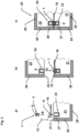
Fig. 3a ), b) und c) drei Schritte des Herstellungsverfahrens eines Elektronikmoduls. - In der
Figur 1a ) ist der Rastbolzen 1 als Seitenansicht gezeigt, der einen unteren ersten Bolzenabschnitt 2, einen oberen zweiten Bolzenabschnitt 3 und einen dazwischen angeordneten Auflageabschnitt 4 aufweist, der einen größeren Durchmesser als die beiden Bolzenabschnitte 2, 3 aufweist. Der Rastbolzen 1, gemäß denFiguren 1a) und Figur 1b ) ist zur Hochachse Z rotationssymmetrisch ausgebildet, wobei die Erfindung hierauf nicht eingeschränkt ist. Beide Bolzenabschnitte 2, 3 weisen jeweils ein Kopfende 5, 6 auf, das jeweils mit einem Halsabschnitt 7, 8 mit dem Auflageabschnitt 4 verbunden ist. Beide Kopfenden 5, 6 sind als pilzkopf- oder kappenartige Erweiterungen der jeweiligen Halsabschnitte 7, 8 ausgeformt und weisen an ihrem unteren, dem Auflageabschnitt 4 zugewandten Ende eine Schneidkante 5.1, 6.1 auf. An dem ersten Bolzenabschnitt 2, der die doppelte Länge des zweiten Bolzenabschnitts 3 aufweist, ist ein Schneid- und/oder Reibkranz 9 angeordnet, dessen umlaufende Oberfläche zum freien Ende hin in Richtung der Achse Z geneigt ist, um die Einführung in ein Aufnahmeelement 23 zu erleichtern. An seinem unteren, dem Auflageelement 4 zugewandten Seite weist dieser eine Schneidkante 9.1 auf. -
Figur 1b ) zeigt den Rastbolzen 1 gemäßFigur 1a ) in der Einbaulage. Der erste Bolzenabschnitt 2 des Rastbolzens 1 ist durch die Durchführungsöffnung 11 der Leiterplatte 10 und in die Öffnung 23.1 des Aufnahmeelementes 3 geführt. Der Auflageabschnitt 4 presst die Leiterplatte 10 auf die Oberkante des Aufnahmeelements 23 des nicht weiter gezeigten Gehäuseunterteils 21 (Fig. 3 ), während die Schneidkante 6.1 des Kopfendes 6 und die Schneidkante 9.1 des Schneid- und Reibkranzes 9 in die Innenwand 23.2 des Aufnahmeelements 23 schneiden und somit kraft- und formschlüssig festgelegt sind und nur noch zerstörend gelöst werden können. Das obere Kopfende 5 des zweiten Bolzenabschnitts 3 ist noch frei, so dass hierauf ein Gehäuseoberteil 22, bzw. dessen Aufnahmeelemente 24 angebracht und befestigt werden können, wie inFigur 3 gezeigt. - In den
Figuren 2a) und 2b ) sind weitere Ausführungsformen des Rastbolzens 1 gezeigt, denen gemeinsam ist, dass kein pilz- oder kappenartiger Kopf ausgebildet ist, sondern eine Mehrzahl von Schneid- und/oder Reibkränzen 9, 14, 15, 16 vorgesehen sind. In dem Ausführungsbeispiel nachFigur 2a ) sind am unteren, ersten Bolzenabschnitt 2 drei umlaufende, parallele Schneid- und/oder Reibkränze 9 und am oberen, zweiten Bolzenabschnitt 3, zwei umlaufende, parallele Schneid- und/oder Reibkränze 14 angeordnet. Von diesen ist der jeweils tiefste mit einer Oberflächenrändelung versehen, was durch die Punktierung der Fläche angedeutet wurde. Wie in derFigur 2b ) beispielhaft dargestellt, können die Schneid- und/oder Reibkränze auch unterbrochen oder zahn- oder krallenartig ausgebildet sein, wie für die drei der Schneid- und/oder Reibkränze 15, 16 dargestellt. Diese bestehen aus einer Mehrzahl umlaufend angeordneter Zahl- oder Krallenelemente. Bei nicht dargestellten Ausführungsvarianten sind die beiden Bolzenabschnitte 2, 3 identisch ausgeformt, so dass der Rastbolzen 1 insgesamt symmetrisch ausgeformt ist. - Der Rastbolzen 1 übernimmt somit zwei Funktionen, indem der einerseits die Leiterplatte 11 (Platine) hält und weiterhin auch das Gehäuseoberteil 22 fixiert. Anders ausgedrückt, er fungiert als eine Art Sandwichverbinder, der die beiden Gehäusehälften aus Gehäuseoberteil 22 und Gehäuseunterteil 21 verbindet und im vorherigen Montageschritt noch zusätzlich auch die Leiterplatte 11 (Platine) dauerhaft (unlösbar) arretiert.
- Der Rastbolzen 1 übernimmt somit im Montageschritt die Fixierung und Positionierung zwischen Gehäuseunterteil 21 und Leiterplatte 11, währen das Gehäuseoberteil 22 herangeführt und unter Krafteinwirkung aufgepresst wird. Weiter übernimmt der Rastbolzen 1 die dauerhafte Verbindung dieser Teile, weil er in dem fertigen Modulgehäuse 20 verbleibt.
- In der
Figur 3a ) werden die ersten Schritte des Herstellverfahrens dargestellt. Das Gehäuseunterteil 21 wird bereitgestellt und die Leiterplatte 10 von oben in Richtung des Pfeils A fluchtend mit den Öffnungen 11 auf den Aufnahmeelementen 23 aufgelegt, wovon nur eines dargestellt ist. Das Aufnahmeelemente 23 ist an einem stegartigen Tragelemente 27 an der Gehäusewand 25 angebracht. Anschließend wird in Richtung B der Rastbolzen 1 herangeführt und eingepresst, so dass die Leiterplatte 10 auf dem Aufnahmeelement 23 fixiert ist. Zeitgleich mit vorgenannten Schritten oder nachlaufend wird in dem zeigten Beispiel ein flüssiges Dicht- und Klebemittel 12 auf den Gehäuserand 21.1 des Gehäuseunterteils 21 aufgetragen. In einer nicht gezeigten Ausführungsform kann der Gehäuserand bzw. die Gehäusewand auch eine Nut- und Federform aufweisen, so dass ein Dicht- und Klebemittel 12 beispielsweise in die Nut eingegossen wird. Alternativ, in einer nicht darstellten Herstellungsvariante, wird das Klebemittel auf dem Gehäuseoberteil 22 aufgetragen. - Nach Abschluss der Schritte gem. der
Figur 3a ) wird, wie inFigur 3b ) dargestellt, das Gehäuseoberteil 22 von oben in Richtung D herangeführt, wobei die Richtung D der Achsrichtung Z des eingefügten Rastbolzens 1 entspricht. Das Gehäuseoberteil 22 wird auf alle Kopfteile 5 der zweiten Bolzenabschnitte 3 aufgepresst, wobei die angeschrägte oder runde Kopfform eine automatische Zentrierung des gesamten Gehäuseoberteils 22 sowie dessen Aufnahmeelemente 24 ermöglicht.Figur 3c ) zeigt schließlich das verschlossene Elektronikmodul 20, bei dem die beiden Aufnahmeelemente 23, 24, welche über stegartige Tragelemente 27, 28 an den jeweiligen Gehäusewänden 25, 26 durch die eingepressten Rastbolzen 1 die beiden Gehäuseteile dichten aufeinanderpressen. Parallel und ohne zusätzliche Befestigungsmittel, wird die Leiterplatte 10 gehalten und zentriert. - Bei einer nicht gezeigten Ausführungsvariante sind die Aufnahmeelemente 23, 24 alleinig oder zusätzlich an der Gehäusedecke 29 angebracht oder diese ist abschnittsweise als Aufnahmeelemente 23, 24 ausgeformt. Die Aufnahmeelemente 23, 24 können insbesondere ein- oder mehrteilige Hülsen sein.
-
- 1
- Rastbolzen
- 2
- Bolzenabschnitt, erster
- 3
- Bolzenabschnitt, zweiter
- 4
- Auflageabschnitt
- 5
- Kopfende, zweites
- 5.1
- Schneidkranz
- 6
- Kopfende, erstes
- 6.1
- Schneidkante
- 7
- Halsabschnitt, erster
- 8
- Halsabschnitt, zweiter
- 9
- Schneid- und/oder ring
- 9.1
- Schneidkante
- 10
- Leiterplatte
- 11
- Durchführungsöffnung
- 12
- Dicht- oder Klebematerial
- 14
- Schneid- und Reibkranz
- 15
- Schneid- und Reibkranz
- 20
- Modulgehäuse
- 21
- Gehäuseunterteil
- 21.1
- Gehäuserand
- 22
- Gehäuseoberteil
- 22.1
- Gehäuserand
- 23
- Aufnahmeelement
- 23.1
- Öffnung
- 23.2
- Innenwand
- 24
- Aufnahmeelement
- 25
- Gehäusewand
- 26
- Gehäusewand
- 27
- Tragelement
- 28
- Tragelement
- A, B, D
- Richtungen
- Z
- Achse, Symmetrieachse
Claims (11)
- Elektronikmodul (20), umfassend ein Gehäuseunterteil (21), eine Leiterplatte (10), ein Befestigungsmittel und ein Gehäuseoberteil (22), wobei die Leiterplatte (10) mindestens eine Durchführungsöffnung (11) zur Befestigung mit dem Befestigungsmittel aufweist, welches mit einem ersten Ende durch die Durchführungsöffnung (11) in ein fluchtend angeordnetes Aufnahmeelement (23) des Gehäuseunterteils (21) kraft- und/oder formschlüssig eingebracht und befestigt ist, wobei am Gehäuseoberteil (22) ein zum Aufnahmeelement (23) des Gehäuseunterteils (21) fluchtend angeordnetes Aufnahmeelement (24) vorgesehen ist, wobei das andere Ende des Befestigungsmittels kraft- und/oder formschlüssig in das mindestens eine Aufnahmeelement (23) des Gehäuseoberteils (22) eingebracht und befestigt ist, wobei das Befestigungsmittel als Rastbolzen (1) ausgeführt ist, umfassend mindestens einen auskragenden Auflageabschnitt (4) und einen ersten Bolzenabschnitt (2) mit einem Kopfende (6) und einem verbindenden Halsabschnitt (8), wobei mindestens ein ein- oder mehrteiliger Schneid- und/oder Reibkranz (6.1, 9.1) im Bereich des Kopfendes (6) und/oder des Halsabschnittes (8) angeordnet ist, wobei ein zweiter Bolzenabschnitt (3) an der Rückseite des auskragenden Auflageabschnitts (4) angeordnet ist, wobei der zweite Bolzenabschnitt (3) ein Kopfende (5) und einen verbindenden Halsabschnitt (7) aufweist, und wobei mindestens ein ein- oder mehrteiliger Schneid- und/oder Reibkranz (5.1) im Bereich des Kopfendes (5) und/oder des Halsabschnittes (7) angeordnet ist, und dadurch gekennzeichnet, dass die Leiterplatte (10) durch den auskragenden Auflageabschnitt (4) des Rastbolzens (1) auf den Aufnahmeelementen (23) des Gehäuseunterteils (21) zentriert und dauerhaft aufgepresst ist.
- Elektronikmodul (20) nach Anspruch 1, dadurch gekennzeichnet, dass der zweite Bolzenabschnitt (3) des Rastbolzens (1) kürzer als der erste Bolzenabschnitt (2) ausgeführt ist, insbesondere die Länge des zweiten Bolzenabschnitts (3) das 0,25fache bis 0,75fache des ersten Bolzenabschnitts (2) beträgt.
- Elektronikmodul (20) nach einem der Ansprüche 1 oder 2, dadurch gekennzeichnet, dass der Rastbolzen (1) an mindestens einem der Kopfenden (5, 6) als pilzkopf- und/oder kappenartige Erweiterung ausgeführt ist, dessen umlaufende Unterkante als Schneidkranz (5.1, 6.1) ausgeführt ist.
- Elektronikmodul (20) nach einem der vorherigen Ansprüche, dadurch gekennzeichnet, dass an mindestens einem Halsabschnitt (7, 8) des Rastbolzens (1) ein ein- oder mehrteiliger Schneid- und/oder Reibkranz (9, 14, 15) angeordnet ist.
- Elektronikmodul (20) nach einem der vorherigen Ansprüche, dadurch gekennzeichnet, dass der Rastbolzen (1) aus einem Metall, insbesondere einem nicht-rostenden Metall oder einem Kunststoff ist, insbesondere einen PVC, PP, PET oder POM hergestellt ist.
- Elektronikmodul (20) nach einem der vorherigen Ansprüche, dadurch gekennzeichnet, dass das Gehäuseoberteil (22) und das Gehäuseunterteil (21) einen Rand (21.1, 22.1) aufweisen, wobei die Ränder (21.1, 22.1) mindestens abschnittsweise miteinander verklebt sind, insbesondere auf der gesamten Länge miteinander verklebt sind.
- Elektronikmodul (20) nach einem der vorherigen Ansprüche, dadurch gekennzeichnet, dass das mindestens zwischen einer Gehäusewand (25, 26) und einem der Aufnahmeelemente (23, 24) ein stegartiges Tragelement (27, 28) angeordnet ist.
- Elektronikmodul (20) nach einem der vorherigen Ansprüche, dadurch gekennzeichnet, dass mindestens ein Aufnahmeelement (23, 24) säulen- und/oder hülsenartig ausgebildet und auf einer Gehäusedecke (29) angebracht ist und/oder die Gehäusedecke (29) abschnittsweise als säulen- und/oder hülsenartiges Aufnahmeelement (23, 24) ausgebildet ist.
- Herstellverfahren für ein Elektronikmodul (20), bei welchem eine mindestens eine Durchführungsöffnung (11) aufweisende Leiterplatte (10) in einem Gehäuseunterteil (21) mit Befestigungsmitteln an mindestens einem Aufnahmeelement (23, 24) angebracht und anschließend ein Gehäuseoberteil (22) befestigt wird, dadurch gekennzeichnet, dass das die folgenden Schritt vorgenommen werden:a) Bereitstellung des Gehäuseunterteils (21)b) Auflage der Leiterplatte (10) auf das mindestens eine Aufnahmeelemente (23) des Gehäuseunterteils (21),c) Durchführen des mindestens einen Befestigungsmittels durch die Durchführungsöffnung (11) und einpressen in das mindestens eine Aufnahmeelement (23), wobei das Elektronikmodul (20) mit dem Befestigungsmittel als ein Rastbolzen (1) nach einem der Ansprüche 1 bis 8 ausgebildet ist undd) Einpressen des Kopfendes (6) des zweiten Bolzenabschnitts (3) in mindestens ein Aufnahmeelement (24) des Gehäuseoberteils (22).
- Herstellverfahren nach Anspruch 9, dadurch gekennzeichnet, dass vor Schritt d) ein Dicht- oder Klebematerial (12) mindestens abschnittsweise auf einen Gehäuserand (21.1, 22.1) aufgebracht und/oder -gelegt wird.
- Herstellverfahren nach einem der Ansprüche 9 oder 10, dadurch gekennzeichnet, dass mindestens jeweils ein Schneid- und/oder Reibkranz (5.1, 6.1, 9, 9.1, 14, 15) in jedem Aufnahmeelement (23, 24) des Gehäuseober- und -unterteil form- und/oder kraftschlüssig eingepresst wird.
Applications Claiming Priority (1)
| Application Number | Priority Date | Filing Date | Title |
|---|---|---|---|
| DE102021116940.2A DE102021116940A1 (de) | 2021-07-01 | 2021-07-01 | Rastbolzen, Elektronikmodul und Herstellverfahren |
Publications (2)
| Publication Number | Publication Date |
|---|---|
| EP4112949A1 EP4112949A1 (de) | 2023-01-04 |
| EP4112949B1 true EP4112949B1 (de) | 2024-12-25 |
Family
ID=81940751
Family Applications (1)
| Application Number | Title | Priority Date | Filing Date |
|---|---|---|---|
| EP22177196.7A Active EP4112949B1 (de) | 2021-07-01 | 2022-06-03 | Elektronikmodul und herstellverfahren |
Country Status (4)
| Country | Link |
|---|---|
| US (1) | US11785727B2 (de) |
| EP (1) | EP4112949B1 (de) |
| CN (2) | CN218416862U (de) |
| DE (1) | DE102021116940A1 (de) |
Families Citing this family (3)
| Publication number | Priority date | Publication date | Assignee | Title |
|---|---|---|---|---|
| DE202020103699U1 (de) | 2020-06-26 | 2021-09-28 | Schlüter-Systems Kg | Dehnungsfugenprofilsystem |
| DE202021100478U1 (de) * | 2021-02-01 | 2022-05-03 | Schlüter-Systems Kg | Profilsystem |
| DE102021116940A1 (de) * | 2021-07-01 | 2023-01-05 | Turck Holding Gmbh | Rastbolzen, Elektronikmodul und Herstellverfahren |
Family Cites Families (20)
| Publication number | Priority date | Publication date | Assignee | Title |
|---|---|---|---|---|
| CH586805A5 (de) * | 1974-01-15 | 1977-04-15 | Europatent Sa | |
| DE9110871U1 (de) | 1991-09-02 | 1991-10-24 | Siemens AG, 8000 München | Gehäuse für elektronische Schaltungsanordnungen, insbesondere für Flachbaugruppen |
| DE9214673U1 (de) | 1992-10-29 | 1992-12-10 | Albert Ackermann GmbH & Co. KG, 51643 Gummersbach | Leiterplattengehäuse |
| US5535100A (en) * | 1995-06-07 | 1996-07-09 | International Business Machines Corporation | Snap-together/quick-release fastening assembly for supporting a circuit card |
| DE20115670U1 (de) * | 2001-09-24 | 2002-02-21 | TRW Automotive Electronics & Components GmbH & Co. KG, 78315 Radolfzell | Gehäuse für ein elektronisches Steuergerät in Fahrzeugen |
| DE10315432A1 (de) | 2003-04-03 | 2004-10-14 | Conti Temic Microelectronic Gmbh | Anordnung zum elektrischen Verbinden |
| DE102010063151A1 (de) | 2010-12-15 | 2012-06-21 | Robert Bosch Gmbh | Steuergerät und Verfahren zum Herstellen eines Steuergeräts |
| US9042105B2 (en) * | 2012-06-21 | 2015-05-26 | Apple Inc. | Electronic devices with printed circuit boards having padded openings |
| DE102012222674A1 (de) * | 2012-12-10 | 2014-06-12 | Robert Bosch Gmbh | Elektronische Anordnung mit Leiterplatte |
| DE102014213243B4 (de) * | 2014-07-08 | 2024-10-17 | Vitesco Technologies GmbH | Gehäuse für ein Steuergerät |
| DE102014218528A1 (de) * | 2014-09-16 | 2016-03-17 | Continental Automotive Gmbh | Gehäuse zur Aufnahme elektrischer und/oder elektronischer Bauteile, elektronisches Steuergerät und Verfahren zur Herstellung derselben |
| EP3073810B1 (de) * | 2015-03-26 | 2021-10-06 | Vitesco Technologies GmbH | Elektronische steuereinheit mit gehäusestabilisierungselement und gehäuse für elektronische steuereinheit |
| US10111353B2 (en) * | 2016-02-26 | 2018-10-23 | Lear Corporation | Electrical unit |
| JP6404258B2 (ja) * | 2016-04-26 | 2018-10-10 | 矢崎総業株式会社 | 電気接続箱及びワイヤハーネス |
| US10159157B2 (en) * | 2016-08-08 | 2018-12-18 | Continental Automotive Systems, Inc. | Compliant PCB-to-housing fastener |
| JP2020009978A (ja) | 2018-07-12 | 2020-01-16 | 東京エレクトロン株式会社 | 回路装置、テスタ、検査装置及び回路基板の反り調整方法 |
| US11122698B2 (en) * | 2018-11-06 | 2021-09-14 | N2 Imaging Systems, LLC | Low stress electronic board retainers and assemblies |
| CN112449538A (zh) * | 2019-08-28 | 2021-03-05 | 高准有限公司 | 用于电子产品的灌封工艺的电路板支撑组件和电子产品 |
| CN211297420U (zh) * | 2020-01-07 | 2020-08-18 | 高准有限公司 | 电路板支撑组件和电子产品 |
| DE102021116940A1 (de) * | 2021-07-01 | 2023-01-05 | Turck Holding Gmbh | Rastbolzen, Elektronikmodul und Herstellverfahren |
-
2021
- 2021-07-01 DE DE102021116940.2A patent/DE102021116940A1/de active Pending
-
2022
- 2022-05-23 CN CN202221243964.5U patent/CN218416862U/zh active Active
- 2022-05-23 CN CN202210563020.4A patent/CN114885548B/zh active Active
- 2022-06-03 EP EP22177196.7A patent/EP4112949B1/de active Active
- 2022-06-28 US US17/809,355 patent/US11785727B2/en active Active
Also Published As
| Publication number | Publication date |
|---|---|
| EP4112949A1 (de) | 2023-01-04 |
| CN218416862U (zh) | 2023-01-31 |
| US20230007790A1 (en) | 2023-01-05 |
| DE102021116940A1 (de) | 2023-01-05 |
| CN114885548B (zh) | 2025-05-13 |
| CN114885548A (zh) | 2022-08-09 |
| US11785727B2 (en) | 2023-10-10 |
Similar Documents
| Publication | Publication Date | Title |
|---|---|---|
| DE19539685B4 (de) | Verbindungseinheit, Verbindungsverfahren und Niet zu ihrer Herstellung | |
| EP1958825B1 (de) | Befestigungsvorrichtung | |
| EP1068458B1 (de) | Verbindungseinrichtung zum verbinden zweier bauteile, kombination der verbindungseinrichtung mit den beiden bauteilen und verfahren zur herstellung einer verbindung zwischen zwei bauteilen | |
| WO1994007040A1 (de) | Vorrichtung zum verbinden von wenigstens zwei elementen | |
| DE102012203946B4 (de) | Elektrische Maschine zum motorischen Verstellen beweglicher Teile im Kraftfahrzeug, sowie Verfahren zum Herstellen der elektrischen Maschine | |
| EP4112949A1 (de) | Rastbolzen, elektronikmodul und herstellverfahren | |
| DE2736012A1 (de) | Befestiger zur befestigung eines teils an plattenmaterial | |
| CH708745A1 (de) | Spanneinrichtung. | |
| DE2610200A1 (de) | Beschlag zum loesbaren verbinden von bauteilen, insbesondere zum wieder loesbaren verbinden von plattenfoermigen bauteilen | |
| EP3529868B1 (de) | Verbindungsanordnung für die verbindung von zwei schaltschrankrahmengestellen | |
| EP3228879B1 (de) | Verbindungsbeschlag, anordnung und verfahren zum verbinden von zwei leichtbauplatten | |
| EP1763639B1 (de) | BEFESTINGUNGSANORDNUNGEN& xA; | |
| DE102013208494A1 (de) | Vorrichtung zur werkzeuglosen Verbindung zweier Bauteile | |
| DE1475032B1 (de) | Formschluessig an einer platte festzuhaltendes bauteil zur aufnahme eines bolzen | |
| EP3736464A1 (de) | Abstandhalter für eine befestigungsanordnung, befestigungsanordnung mit einem solchen abstandhalter sowie verfahren zum befestigen eines montageteils an einem trägerteil | |
| DE202009013312U1 (de) | Verbindungsvorrichtung | |
| DE102006028816B4 (de) | Verfahren zum getakteten, kontinuierlichen Herstellen von beidseitig umspritzten flexiblen Leiterplatten | |
| WO1994004015A1 (de) | Adaptereinrichtung für eine automatische prüfvorrichtung zur prüfen von schaltungsplatinen | |
| DE10240624A1 (de) | Verfahren zum Abschließen eines Drosselklappenstutzens | |
| DE102010061301A1 (de) | Verbindungselement für ein Faserverbundbauteil | |
| DE202021101300U1 (de) | Befestigungsplattenanordnung | |
| DE102005003186A1 (de) | Vorrichtung zum Verbinden von Bauelementen | |
| EP4686838A1 (de) | Verbinder, anordnung, verfahren zum verbinden und verwendung eines verbinders | |
| DE1902238B2 (de) | Befestigungselement aus kunststoff | |
| DE102005023124A1 (de) | Steck-Dreh-Verbindung |
Legal Events
| Date | Code | Title | Description |
|---|---|---|---|
| PUAI | Public reference made under article 153(3) epc to a published international application that has entered the european phase |
Free format text: ORIGINAL CODE: 0009012 |
|
| STAA | Information on the status of an ep patent application or granted ep patent |
Free format text: STATUS: THE APPLICATION HAS BEEN PUBLISHED |
|
| AK | Designated contracting states |
Kind code of ref document: A1 Designated state(s): AL AT BE BG CH CY CZ DE DK EE ES FI FR GB GR HR HU IE IS IT LI LT LU LV MC MK MT NL NO PL PT RO RS SE SI SK SM TR |
|
| STAA | Information on the status of an ep patent application or granted ep patent |
Free format text: STATUS: REQUEST FOR EXAMINATION WAS MADE |
|
| 17P | Request for examination filed |
Effective date: 20230223 |
|
| RBV | Designated contracting states (corrected) |
Designated state(s): AL AT BE BG CH CY CZ DE DK EE ES FI FR GB GR HR HU IE IS IT LI LT LU LV MC MK MT NL NO PL PT RO RS SE SI SK SM TR |
|
| GRAP | Despatch of communication of intention to grant a patent |
Free format text: ORIGINAL CODE: EPIDOSNIGR1 |
|
| STAA | Information on the status of an ep patent application or granted ep patent |
Free format text: STATUS: GRANT OF PATENT IS INTENDED |
|
| INTG | Intention to grant announced |
Effective date: 20240726 |
|
| P01 | Opt-out of the competence of the unified patent court (upc) registered |
Free format text: CASE NUMBER: APP_55103/2024 Effective date: 20241007 |
|
| GRAS | Grant fee paid |
Free format text: ORIGINAL CODE: EPIDOSNIGR3 |
|
| GRAA | (expected) grant |
Free format text: ORIGINAL CODE: 0009210 |
|
| STAA | Information on the status of an ep patent application or granted ep patent |
Free format text: STATUS: THE PATENT HAS BEEN GRANTED |
|
| AK | Designated contracting states |
Kind code of ref document: B1 Designated state(s): AL AT BE BG CH CY CZ DE DK EE ES FI FR GB GR HR HU IE IS IT LI LT LU LV MC MK MT NL NO PL PT RO RS SE SI SK SM TR |
|
| REG | Reference to a national code |
Ref country code: GB Ref legal event code: FG4D Free format text: NOT ENGLISH |
|
| REG | Reference to a national code |
Ref country code: CH Ref legal event code: EP |
|
| REG | Reference to a national code |
Ref country code: DE Ref legal event code: R096 Ref document number: 502022002479 Country of ref document: DE |
|
| REG | Reference to a national code |
Ref country code: IE Ref legal event code: FG4D Free format text: LANGUAGE OF EP DOCUMENT: GERMAN |
|
| REG | Reference to a national code |
Ref country code: LT Ref legal event code: MG9D |
|
| PG25 | Lapsed in a contracting state [announced via postgrant information from national office to epo] |
Ref country code: FI Free format text: LAPSE BECAUSE OF FAILURE TO SUBMIT A TRANSLATION OF THE DESCRIPTION OR TO PAY THE FEE WITHIN THE PRESCRIBED TIME-LIMIT Effective date: 20241225 |
|
| PG25 | Lapsed in a contracting state [announced via postgrant information from national office to epo] |
Ref country code: BG Free format text: LAPSE BECAUSE OF FAILURE TO SUBMIT A TRANSLATION OF THE DESCRIPTION OR TO PAY THE FEE WITHIN THE PRESCRIBED TIME-LIMIT Effective date: 20241225 |
|
| PG25 | Lapsed in a contracting state [announced via postgrant information from national office to epo] |
Ref country code: NO Free format text: LAPSE BECAUSE OF FAILURE TO SUBMIT A TRANSLATION OF THE DESCRIPTION OR TO PAY THE FEE WITHIN THE PRESCRIBED TIME-LIMIT Effective date: 20250325 |
|
| PG25 | Lapsed in a contracting state [announced via postgrant information from national office to epo] |
Ref country code: LV Free format text: LAPSE BECAUSE OF FAILURE TO SUBMIT A TRANSLATION OF THE DESCRIPTION OR TO PAY THE FEE WITHIN THE PRESCRIBED TIME-LIMIT Effective date: 20241225 Ref country code: GR Free format text: LAPSE BECAUSE OF FAILURE TO SUBMIT A TRANSLATION OF THE DESCRIPTION OR TO PAY THE FEE WITHIN THE PRESCRIBED TIME-LIMIT Effective date: 20250326 |
|
| PG25 | Lapsed in a contracting state [announced via postgrant information from national office to epo] |
Ref country code: RS Free format text: LAPSE BECAUSE OF FAILURE TO SUBMIT A TRANSLATION OF THE DESCRIPTION OR TO PAY THE FEE WITHIN THE PRESCRIBED TIME-LIMIT Effective date: 20250325 |
|
| REG | Reference to a national code |
Ref country code: NL Ref legal event code: MP Effective date: 20241225 |
|
| PG25 | Lapsed in a contracting state [announced via postgrant information from national office to epo] |
Ref country code: NL Free format text: LAPSE BECAUSE OF FAILURE TO SUBMIT A TRANSLATION OF THE DESCRIPTION OR TO PAY THE FEE WITHIN THE PRESCRIBED TIME-LIMIT Effective date: 20241225 |
|
| PG25 | Lapsed in a contracting state [announced via postgrant information from national office to epo] |
Ref country code: SM Free format text: LAPSE BECAUSE OF FAILURE TO SUBMIT A TRANSLATION OF THE DESCRIPTION OR TO PAY THE FEE WITHIN THE PRESCRIBED TIME-LIMIT Effective date: 20241225 |
|
| PG25 | Lapsed in a contracting state [announced via postgrant information from national office to epo] |
Ref country code: PL Free format text: LAPSE BECAUSE OF FAILURE TO SUBMIT A TRANSLATION OF THE DESCRIPTION OR TO PAY THE FEE WITHIN THE PRESCRIBED TIME-LIMIT Effective date: 20241225 |
|
| PGFP | Annual fee paid to national office [announced via postgrant information from national office to epo] |
Ref country code: DE Payment date: 20250618 Year of fee payment: 4 |
|
| PG25 | Lapsed in a contracting state [announced via postgrant information from national office to epo] |
Ref country code: ES Free format text: LAPSE BECAUSE OF FAILURE TO SUBMIT A TRANSLATION OF THE DESCRIPTION OR TO PAY THE FEE WITHIN THE PRESCRIBED TIME-LIMIT Effective date: 20241225 |
|
| PG25 | Lapsed in a contracting state [announced via postgrant information from national office to epo] |
Ref country code: IS Free format text: LAPSE BECAUSE OF FAILURE TO SUBMIT A TRANSLATION OF THE DESCRIPTION OR TO PAY THE FEE WITHIN THE PRESCRIBED TIME-LIMIT Effective date: 20250425 |
|
| PG25 | Lapsed in a contracting state [announced via postgrant information from national office to epo] |
Ref country code: PT Free format text: LAPSE BECAUSE OF FAILURE TO SUBMIT A TRANSLATION OF THE DESCRIPTION OR TO PAY THE FEE WITHIN THE PRESCRIBED TIME-LIMIT Effective date: 20250428 |
|
| PG25 | Lapsed in a contracting state [announced via postgrant information from national office to epo] |
Ref country code: EE Free format text: LAPSE BECAUSE OF FAILURE TO SUBMIT A TRANSLATION OF THE DESCRIPTION OR TO PAY THE FEE WITHIN THE PRESCRIBED TIME-LIMIT Effective date: 20241225 |
|
| PGFP | Annual fee paid to national office [announced via postgrant information from national office to epo] |
Ref country code: FR Payment date: 20250626 Year of fee payment: 4 |
|
| PG25 | Lapsed in a contracting state [announced via postgrant information from national office to epo] |
Ref country code: RO Free format text: LAPSE BECAUSE OF FAILURE TO SUBMIT A TRANSLATION OF THE DESCRIPTION OR TO PAY THE FEE WITHIN THE PRESCRIBED TIME-LIMIT Effective date: 20241225 |
|
| PGFP | Annual fee paid to national office [announced via postgrant information from national office to epo] |
Ref country code: AT Payment date: 20250721 Year of fee payment: 4 |
|
| PG25 | Lapsed in a contracting state [announced via postgrant information from national office to epo] |
Ref country code: SK Free format text: LAPSE BECAUSE OF FAILURE TO SUBMIT A TRANSLATION OF THE DESCRIPTION OR TO PAY THE FEE WITHIN THE PRESCRIBED TIME-LIMIT Effective date: 20241225 |
|
| PG25 | Lapsed in a contracting state [announced via postgrant information from national office to epo] |
Ref country code: CZ Free format text: LAPSE BECAUSE OF FAILURE TO SUBMIT A TRANSLATION OF THE DESCRIPTION OR TO PAY THE FEE WITHIN THE PRESCRIBED TIME-LIMIT Effective date: 20241225 |
|
| PG25 | Lapsed in a contracting state [announced via postgrant information from national office to epo] |
Ref country code: IT Free format text: LAPSE BECAUSE OF FAILURE TO SUBMIT A TRANSLATION OF THE DESCRIPTION OR TO PAY THE FEE WITHIN THE PRESCRIBED TIME-LIMIT Effective date: 20241225 |
|
| PG25 | Lapsed in a contracting state [announced via postgrant information from national office to epo] |
Ref country code: SE Free format text: LAPSE BECAUSE OF FAILURE TO SUBMIT A TRANSLATION OF THE DESCRIPTION OR TO PAY THE FEE WITHIN THE PRESCRIBED TIME-LIMIT Effective date: 20241225 |
|
| REG | Reference to a national code |
Ref country code: DE Ref legal event code: R097 Ref document number: 502022002479 Country of ref document: DE |
|
| PG25 | Lapsed in a contracting state [announced via postgrant information from national office to epo] |
Ref country code: DK Free format text: LAPSE BECAUSE OF FAILURE TO SUBMIT A TRANSLATION OF THE DESCRIPTION OR TO PAY THE FEE WITHIN THE PRESCRIBED TIME-LIMIT Effective date: 20241225 |
|
| PLBE | No opposition filed within time limit |
Free format text: ORIGINAL CODE: 0009261 |
|
| STAA | Information on the status of an ep patent application or granted ep patent |
Free format text: STATUS: NO OPPOSITION FILED WITHIN TIME LIMIT |
|
| REG | Reference to a national code |
Ref country code: CH Ref legal event code: L10 Free format text: ST27 STATUS EVENT CODE: U-0-0-L10-L00 (AS PROVIDED BY THE NATIONAL OFFICE) Effective date: 20251105 |
|
| 26N | No opposition filed |
Effective date: 20250926 |
|
| REG | Reference to a national code |
Ref country code: CH Ref legal event code: H13 Free format text: ST27 STATUS EVENT CODE: U-0-0-H10-H13 (AS PROVIDED BY THE NATIONAL OFFICE) Effective date: 20260127 |
|
| PG25 | Lapsed in a contracting state [announced via postgrant information from national office to epo] |
Ref country code: MC Free format text: LAPSE BECAUSE OF FAILURE TO SUBMIT A TRANSLATION OF THE DESCRIPTION OR TO PAY THE FEE WITHIN THE PRESCRIBED TIME-LIMIT Effective date: 20241225 |
|
| PG25 | Lapsed in a contracting state [announced via postgrant information from national office to epo] |
Ref country code: LU Free format text: LAPSE BECAUSE OF NON-PAYMENT OF DUE FEES Effective date: 20250603 |
|
| REG | Reference to a national code |
Ref country code: BE Ref legal event code: MM Effective date: 20250630 |
|
| PG25 | Lapsed in a contracting state [announced via postgrant information from national office to epo] |
Ref country code: IE Free format text: LAPSE BECAUSE OF NON-PAYMENT OF DUE FEES Effective date: 20250603 |
|
| PG25 | Lapsed in a contracting state [announced via postgrant information from national office to epo] |
Ref country code: HR Free format text: LAPSE BECAUSE OF FAILURE TO SUBMIT A TRANSLATION OF THE DESCRIPTION OR TO PAY THE FEE WITHIN THE PRESCRIBED TIME-LIMIT Effective date: 20241225 |
|
| PG25 | Lapsed in a contracting state [announced via postgrant information from national office to epo] |
Ref country code: BE Free format text: LAPSE BECAUSE OF NON-PAYMENT OF DUE FEES Effective date: 20250630 |
|
| PG25 | Lapsed in a contracting state [announced via postgrant information from national office to epo] |
Ref country code: CH Free format text: LAPSE BECAUSE OF NON-PAYMENT OF DUE FEES Effective date: 20250630 |