EP4176463B1 - Substrat support pour structure soi et procede de fabrication associe - Google Patents
Substrat support pour structure soi et procede de fabrication associe Download PDFInfo
- Publication number
- EP4176463B1 EP4176463B1 EP21720818.0A EP21720818A EP4176463B1 EP 4176463 B1 EP4176463 B1 EP 4176463B1 EP 21720818 A EP21720818 A EP 21720818A EP 4176463 B1 EP4176463 B1 EP 4176463B1
- Authority
- EP
- European Patent Office
- Prior art keywords
- support substrate
- microns
- region
- substrate
- equal
- Prior art date
- Legal status (The legal status is an assumption and is not a legal conclusion. Google has not performed a legal analysis and makes no representation as to the accuracy of the status listed.)
- Active
Links
Images
Classifications
-
- H—ELECTRICITY
- H10—SEMICONDUCTOR DEVICES; ELECTRIC SOLID-STATE DEVICES NOT OTHERWISE PROVIDED FOR
- H10P—GENERIC PROCESSES OR APPARATUS FOR THE MANUFACTURE OR TREATMENT OF DEVICES COVERED BY CLASS H10
- H10P36/00—Gettering within semiconductor bodies
- H10P36/20—Intrinsic gettering, i.e. thermally inducing defects by using oxygen present in the silicon body
-
- H—ELECTRICITY
- H10—SEMICONDUCTOR DEVICES; ELECTRIC SOLID-STATE DEVICES NOT OTHERWISE PROVIDED FOR
- H10P—GENERIC PROCESSES OR APPARATUS FOR THE MANUFACTURE OR TREATMENT OF DEVICES COVERED BY CLASS H10
- H10P72/00—Handling or holding of wafers, substrates or devices during manufacture or treatment thereof
- H10P72/70—Handling or holding of wafers, substrates or devices during manufacture or treatment thereof for supporting or gripping
- H10P72/74—Handling or holding of wafers, substrates or devices during manufacture or treatment thereof for supporting or gripping using temporarily an auxiliary support
-
- H—ELECTRICITY
- H10—SEMICONDUCTOR DEVICES; ELECTRIC SOLID-STATE DEVICES NOT OTHERWISE PROVIDED FOR
- H10D—INORGANIC ELECTRIC SEMICONDUCTOR DEVICES
- H10D86/00—Integrated devices formed in or on insulating or conducting substrates, e.g. formed in silicon-on-insulator [SOI] substrates or on stainless steel or glass substrates
- H10D86/201—Integrated devices formed in or on insulating or conducting substrates, e.g. formed in silicon-on-insulator [SOI] substrates or on stainless steel or glass substrates the substrates comprising an insulating layer on a semiconductor body, e.g. SOI
-
- H—ELECTRICITY
- H10—SEMICONDUCTOR DEVICES; ELECTRIC SOLID-STATE DEVICES NOT OTHERWISE PROVIDED FOR
- H10P—GENERIC PROCESSES OR APPARATUS FOR THE MANUFACTURE OR TREATMENT OF DEVICES COVERED BY CLASS H10
- H10P36/00—Gettering within semiconductor bodies
- H10P36/03—Gettering within semiconductor bodies within silicon bodies
- H10P36/07—Gettering within semiconductor bodies within silicon bodies of silicon-on-insulator structures
-
- H—ELECTRICITY
- H10—SEMICONDUCTOR DEVICES; ELECTRIC SOLID-STATE DEVICES NOT OTHERWISE PROVIDED FOR
- H10P—GENERIC PROCESSES OR APPARATUS FOR THE MANUFACTURE OR TREATMENT OF DEVICES COVERED BY CLASS H10
- H10P90/00—Preparation of wafers not covered by a single main group of this subclass, e.g. wafer reinforcement
-
- H—ELECTRICITY
- H10—SEMICONDUCTOR DEVICES; ELECTRIC SOLID-STATE DEVICES NOT OTHERWISE PROVIDED FOR
- H10P—GENERIC PROCESSES OR APPARATUS FOR THE MANUFACTURE OR TREATMENT OF DEVICES COVERED BY CLASS H10
- H10P90/00—Preparation of wafers not covered by a single main group of this subclass, e.g. wafer reinforcement
- H10P90/19—Preparing inhomogeneous wafers
- H10P90/1904—Preparing vertically inhomogeneous wafers
- H10P90/1906—Preparing SOI wafers
- H10P90/1914—Preparing SOI wafers using bonding
- H10P90/1916—Preparing SOI wafers using bonding with separation or delamination along an ion implanted layer, e.g. Smart-cut
-
- H—ELECTRICITY
- H10—SEMICONDUCTOR DEVICES; ELECTRIC SOLID-STATE DEVICES NOT OTHERWISE PROVIDED FOR
- H10P—GENERIC PROCESSES OR APPARATUS FOR THE MANUFACTURE OR TREATMENT OF DEVICES COVERED BY CLASS H10
- H10P95/00—Generic processes or apparatus for manufacture or treatments not covered by the other groups of this subclass
- H10P95/90—Thermal treatments, e.g. annealing or sintering
-
- H—ELECTRICITY
- H10—SEMICONDUCTOR DEVICES; ELECTRIC SOLID-STATE DEVICES NOT OTHERWISE PROVIDED FOR
- H10W—GENERIC PACKAGES, INTERCONNECTIONS, CONNECTORS OR OTHER CONSTRUCTIONAL DETAILS OF DEVICES COVERED BY CLASS H10
- H10W10/00—Isolation regions in semiconductor bodies between components of integrated devices
- H10W10/10—Isolation regions comprising dielectric materials
- H10W10/181—Semiconductor-on-insulator [SOI] isolation regions, e.g. buried oxide regions of SOI wafers
-
- H—ELECTRICITY
- H10—SEMICONDUCTOR DEVICES; ELECTRIC SOLID-STATE DEVICES NOT OTHERWISE PROVIDED FOR
- H10P—GENERIC PROCESSES OR APPARATUS FOR THE MANUFACTURE OR TREATMENT OF DEVICES COVERED BY CLASS H10
- H10P95/00—Generic processes or apparatus for manufacture or treatments not covered by the other groups of this subclass
- H10P95/90—Thermal treatments, e.g. annealing or sintering
- H10P95/906—Thermal treatments, e.g. annealing or sintering for altering the shape of semiconductors, e.g. smoothing the surface
Definitions
- the present invention targets the field of semiconductors and microelectronics. It concerns a silicon support substrate for a Silicon on Insulator (SOI) structure, in particular for a completely depleted silicon on insulator (FD-SOI) structure, suitable for logic and radio frequency applications.
- SOI Silicon on Insulator
- FD-SOI completely depleted silicon on insulator
- the invention also relates to a method of manufacturing such a support substrate.
- the FD-SOI structure must meet several criteria.
- the very thin useful layer (typically of the order of 20nm) in silicon must have excellent thickness uniformity, as well as high crystalline quality. For this, it must be able to undergo long-term high temperature treatments, particularly during its manufacturing; said treatments are required to smooth the free surface of the useful layer and cure crystalline defects present in the latter.
- the supporting substrate of the SOI structure is resistant to the slip lines type failure mode, and in particular, that it has a sufficient and homogeneous density of micro-defects (BMD for “bulk micro-defect”) over its entire extent.
- micro-defects are usually present in sufficient quantity in substrates with a high interstitial oxygen content (called “high Oi”), typically corresponding to an Oi concentration greater than 1E18/cm3 (ASTM'79 standard): these support substrates “ high Oi” are particularly robust to slip line type defects.
- high Oi interstitial oxygen content
- the SOI structure must be compatible with very low inspection thresholds, in order to authorize the detection of defects smaller than 50 nm on and/or in the useful layer.
- a support substrate with a high content of interstitial oxygen (Oi) contains defects called “crystal particles of origin” (COP) which limit the inspectability of the useful layer of the SOI structure; in fact, COP defects located in a superficial zone of the support substrate, even if they remain under the buried oxide layer of the SOI structure, are detected during inspection of the useful layer at very high detection thresholds , due to the penetration of the inspection signal which will slightly probe under the buried oxide layer.
- a support substrate with a high Oi content is therefore not compatible, as it stands, with such applications.
- the substrate supporting the SOI structure must have a high resistivity (greater than 500ohm.cm, 1000ohm.cm, or even greater than 5000ohm.cm) and stable.
- a high resistivity greater than 500ohm.cm, 1000ohm.cm, or even greater than 5000ohm.cm
- it is usual to use very resistive support substrates with a low Oi content (called “low Oi”, typically corresponding to an Oi concentration lower than 8E17 Oi/cm 3 ), because those with a high Oi content in Oi show an instability of resistivity at depth, in particular due to the thermal smoothing treatments required for the useful layer.
- support substrates with low Oi content are extremely sensitive to long high temperature treatments and subsequently exhibit a high density of slip lines damaging to the SOI structure.
- EP 1 713 121 A2 discloses a support substrate.
- the present invention proposes a solution remedying all or part of the aforementioned drawbacks. It concerns in particular a support substrate compatible with the thermal treatments imposed on an SOI structure and with the strict specifications of logic and radio frequency applications.
- the invention also relates to a method of manufacturing such a support substrate.
- the invention also relates to an SOI structure comprising a useful layer disposed on a dielectric layer, itself disposed on a support substrate such as above.
- the useful layer may have a thickness of less than 50nm, preferably between 4nm and 25nm; and the dielectric layer may have a thickness of between 10nm and 150nm.
- the invention further relates to an electronic component for low power and radio frequency logic application comprising at least one transistor arranged on and/or in the useful layer of an SOI structure such as above.
- the first sequence of the second heat treatment comprises two temperature plateaus, a first plateau between 650°C and 750°C, and a second plateau around 800°C.
- the figures are schematic representations which, for the purposes of readability, are not to scale.
- the thicknesses of the layers along the z axis are not to scale with respect to the lateral dimensions along the x and y axes.
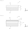
- the invention relates to a support substrate 10 made of monocrystalline silicon, having a front face 10a and a rear face 10b, substantially parallel to a main plane (x,y). It is advantageously presented in the form of a circular plate, with a diameter of between 200mm and 450mm. Its total thickness, along the z axis normal to the main plane (x,y), can vary between a few hundred microns and 1000 microns.
- the support substrate 10 comprises a superficial region 1 extending from the front face 10a to a depth of the order of one micron, typically between 800nm and 2 microns.
- This Surface region 1 has the particularity of a very low density of particles of crystalline origin (COP).
- COP particles of crystalline origin
- the support substrate 10 comprises an upper region 2 extending from the front face 10a to a depth of between a few microns and 40 microns, preferably to a depth of between 10 microns and 30 microns.
- the upper region 2 therefore includes the superficial region 1.
- the upper region 2 has an interstitial oxygen content (Oi) less than or equal to 7.5E17 Oi/cm 3 (equivalent to a content less than or equal to 15 ppma (according to the standard ASTM'79). It also has a resistivity greater than 500 ohm.cm, corresponding to a low concentration of P-type dopant (boron).
- its resistivity is even greater than or equal to 750 ohm.cm, or even greater than or equal to 750 ohm.cm. equal to 1000ohm.cm
- the resistivity level is defined according to the intended application and the electronic components which will subsequently be produced above the support substrate 10.
- the resistivity ranges of the upper region 2 are particularly suitable for radio frequency components. targeting applications in the 30 - 300GHz spectrum, involving millimeter wavelengths ("mmWave”) and which we are talking about in particular to support the 5G network of the next generations of mobile phones.
- the support substrate 10 finally comprises a lower region 3 extending between the upper region 2 and the rear face 10b, the thickness of which is of the order of a few hundred microns.
- This lower region 3 has a concentration of micro-defects (BMD) greater than or equal to 1E8/cm 3 , which gives it great mechanical robustness to heat treatments at high temperatures.
- the concentration of micro-defects (BMD) in the lower region 3 is preferably between 1E8/cm 3 and 3E10/cm 3 , and even more preferably between 1E9/cm 3 and 2E10/cm 3 .
- the lower region 3 has a resistivity typically greater than or equal to 250 ohm.cm and potentially fluctuating, which has no real influence on future radio frequency components because the electromagnetic fields generated by said components do not reach or very marginally. the lower region 3. Only the resistivity of the upper region 2 must have a stable and sufficiently high value.
- the invention therefore also relates to a Silicon on Insulator (SOI) structure 100 comprising a useful layer 30 placed on a dielectric layer 20, itself placed on a aforementioned support substrate 10 ( figure 2 ).
- SOI Silicon on Insulator
- the useful layer 30 is made of high quality monocrystalline silicon and has a thickness of less than 50nm, preferably between 4nm and 25nm. This thickness range is particularly suitable for electronic components based on FD-SOI type technologies and architectures.
- the dielectric layer 20, for example made of carbon dioxide silicon, has a thickness of between 10nm and 150nm.
- the quality of the useful layer 30 can therefore be controlled finely and reliably, without discomfort and/or false detection linked to the presence of COP on the surface of the support substrate 10.
- the invention also relates to an electronic component for low power and radio frequency logic applications.
- a component comprises in particular, at least one transistor arranged on and/or in the useful layer 30 of the SOI structure 100.
- the characteristics of the upper region 2 of the support substrate 10, namely the resistivity and the low Oi concentration, give this region very good insulation performance: in fact, beyond its high level, the resistivity is also stable in this region 2 because it does not undergo fluctuations linked to too high a concentration of Oi, capable of generate thermal oxygen donors and small BMDs compensating for the initial P-type doping.
- the upper region 2 therefore does not undergo a drop or strong fluctuation in resistivity during the high temperature heat treatments (>1100°C) applied to the SOI 100 structure.
- the high density of micro-defects (BMD) in the lower region 3 of the support substrate 10 give the latter excellent mechanical strength and insensitivity to slip line type defects, during said heat treatments.
- the invention further relates to a method of manufacturing a support substrate 10 as previously described.
- the manufacturing process comprises a step a) of supplying an initial substrate 10' of monocrystalline silicon, having an interstitial oxygen content of between 12E17 Oi/cm 3 and 16E17 Oi/cm 3 (equivalent to a content of between 24 and 32 ppma ASTM'79).
- a substrate with a content between 24 and 28 ppma is usually considered to have a medium Oi content (“mid Oi”);
- a substrate with a content between 27 and 32 ppma is usually considered to be high in Oi (“high Oi”).
- the initial substrate 10' has a resistivity greater than 500 ohm.cm, i.e. a concentration of P-type dopants (Boron) less than or equal to 2.6E13/cm 3 . It is intended to form the support substrate 10 after having undergone subsequent steps b) and c) of the process. Thus, the resistivity of the initial substrate 10' is chosen at the required value for the upper region 2 of the support substrate 10, depending on the intended application.
- the resistivity of the initial substrate 10' is greater than or equal to 750 ohm.cm, or even greater than or equal to 1000 ohm.cm.
- a first heat treatment at a temperature between 1150°C and 1250°C, under a neutral or reducing atmosphere is applied to the initial substrate 10'.
- the duration of this treatment is greater than or equal to 30 minutes, for example, between 5 hours and 10 hours.
- This first heat treatment has the role of dissolving particles of crystalline origin (COP) in a superficial region of the initial substrate 10', to a depth of between 800nm and 2 microns. This leads to the formation of the surface region 1 of the future support substrate 10.
- COP crystalline origin
- the dissolution of COPs can for example be carried out by rapid annealing (RTA for “rapid thermal anneal”), at a temperature around 1250°C, for 10 s, under a neutral atmosphere (Argon) or reducing (Argon and Hydrogen), with rapid rise and fall ramps (50°C/min).
- RTA rapid thermal anneal
- annealing in a conventional oven for example at 1200°C, for 30 min or 1 hour, always under a neutral or reducing atmosphere, also makes it possible to dissolve the COPs in the surface region 1.
- the first heat treatment also has the role of exo-diffusing interstitial oxygen (Oi) and of depleting the initial substrate 10' in Oi in a region going from its front face 10a to a more or less significant depth, in depending on the duration of the heat treatment.
- Oi interstitial oxygen
- the substrate is depleted in Oi to a depth of around 20 microns. This leads to the formation of the upper region 2 of the future support substrate 10.
- the first heat treatment can thus consist either of a single annealing, which will play the two roles stated above, or of a sequence of annealings in the same equipment or in different equipment, to achieve the dissolution of the COPs and the exo -diffusion of interstitial oxygen sequentially.
- an intermediate substrate 10" which comprises a superficial region 1 going from the front face 10a to a depth of between 800nm and 2 microns.
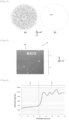
- This superficial region 1 has a very low density of particles of crystalline origin (COP) as illustrated in the figure 4(b) , in comparison with the figure 4(a) which corresponds to the initial substrate 10', before any treatment.
- COP crystalline origin
- the maps of the Figure 4 were carried out using KLA-Tencor SP2 type equipment, in oblique incidence mode and with a detection threshold of 44nm, on wafers of 300mm in diameter: more than 1000 COP at the front face 10a of an initial substrate 10' supplied in step a) of the method; after the first heat treatment of step b), less than ten COPs, or even less than five COPs, are detected at the front face 10a of the intermediate substrate 10" (one COP only in the example of the figure 4(b) ).
- the intermediate substrate 10" also comprises an upper region 2 extending from the front face 10a to a depth of between a few microns and 40 microns, preferably to a depth of between 10 microns and 30 microns.
- the upper region 2 has an interstitial oxygen content (Oi) less than or equal to 7.5E17 Oi/cm 3 , depleted compared to the Oi content of the initial substrate 10', due to the first heat treatment.
- the resistivity of the upper region 2. is that of the initial substrate 10', i.e. greater than 500 ohm.cm
- This upper region 2 can be compared to silicon with a low Oi content (“low Oi”), which gives it excellent stability in terms of resistivity, even when the substrate will be subjected to very high temperatures.
- the manufacturing process then comprises a step c) during which a second heat treatment is applied to the intermediate substrate 10".
- This treatment comprises a first annealing sequence at a temperature between 600°C and 900°C, and a second annealing sequence at a temperature between 950°C and 1100°C.
- the first annealing sequence includes two temperature plateaus.
- a first plateau between 650°C and 750°C lasting between 30min and 10h, under a neutral atmosphere or with low oxygen flow (typically around 0.075 liters per standard minute (slm) of O2 and around 0.015 slm of O2, respectively in an oven for 300mm wafers and an oven for 200mm wafers).
- the role of this first plate is to promote the nucleation of defects called "nuclei", of small size (typically less than 10nm, or even 5nm), in particular in the lower region (under the upper region 2) of the intermediate substrate 10" which includes a high concentration of Oi
- These nuclei are small precipitates of SiOx, initiated either heterogeneously, i.e.
- the second sequence of the second heat treatment lasting between 5 hours and 20 hours, will then cause the diffusion of the interstitial oxygen Oi and its precipitation on the numerous nuclei present in the lower region of the substrate 10", which will make them grow and make them stable in the material.
- the micro-defects thus created are known as BMD for “bulk micro defects”.
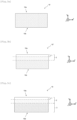
- the lower region 3 of the support substrate 10 rich in BMD micro-defects is thus formed ( figure 3c ).
- a BMD concentration is reached in the lower region 3 of between 1E8/cm 3 and 3E10/cm 3 , and preferably between 1E9/cm 3 and 2E10/cm 3 .
- Figure 5 corresponds to an optical microscope image of the edge of a support substrate 10, after a chemical etching to reveal the BMD micro-defects: we observe a defect-free zone with a thickness of the order of 20-25 microns in the region upper 2.
- the lower region 3 includes a high density of BMD defects, of the order of a few 1E9/cm 3 , typically between 2E9/cm 3 and 5E9/cm 3 in this example.
- FIG. 6 illustrates a resistivity curve as a function of depth for a support substrate 10 according to the invention.
- the initial substrate 10' had a resistivity of around 3500 ohm.cm and a high Oi content.
- the support substrate 10 has a resistivity greater than or equal to 3000 ohm.cm and stable over the first thirty microns (upper region 2).
- the lower region 3 has a very high and fluctuating resistivity, due to the high density of interstitial oxygen. Note that this resistivity can still evolve during the manufacturing processes of the SOI structure and the microelectronic components, while the upper region 2 will retain its level of resistivity and its low COP content (surface region 1).
- Such a support substrate 10 can be used in a process for manufacturing an SOI structure 100 as illustrated in the figure 2 .
- the development of an SOI 100 structure is preferably based on the thin layer transfer process known as the Smart Cut TM process.
- a monocrystalline silicon donor substrate is implanted by its front face, so as to define a buried fragile plane substantially parallel to the front face and delimiting, with the latter, the thin layer 30,20 to be transferred.
- Implantation is usually done with light species such as hydrogen ions, helium ions or a combination of these two species.
- the fragile plane is so named because it includes nano-cracks in lenticular form generated by the implanted light species.
- the thin layer 30,20 to be transferred comprises, from the front face of the donor substrate to the buried fragile plane, a dielectric layer 20 and a silicon layer 30 which will respectively form the buried dielectric layer 20 and the layer useful 30 in silicon of the SOI structure 100.
- the implantation energy of the light species is chosen and adjusted so as to form the buried fragile plane (more or less located at the level of the implantation peak) at the depth corresponding to the desired thickness of useful layer 30, taking into account finishing steps (mentioned below) which consume a part of material of said layer 30.
- the donor substrate and the support substrate 10 are then assembled, by direct bonding between the front faces of said substrates, to form a bonded assembly.
- Surface cleaning and/or activation well known in the field of molecular adhesion bonding, can be applied to the substrates prior to assembly, to obtain excellent bonding quality. Assembly in a controlled atmosphere is also possible.
- Separation at the level of the buried fragile plane is preferably carried out by application of a heat treatment at medium temperature, typically between 350°C and 500°C, due to the growth of microcracks by coalescence and pressurization of the gaseous species.
- the separation can be caused by the application of a mechanical stress to the bonded assembly.
- finishing heat treatments are usually carried out at temperatures between 900°C and 1250°C: the robustness of the lower region 3 of the support substrate 10 to defects such as slip lines and other plastic deformations , is a significant asset during these treatments and makes it possible to maintain very good integrity of the SOI 100 structure.
- the electronic components may in particular consist of RF switches (“switches”), power amplifiers (“power amplifier PA”), low noise amplifiers (“low noise amplifier LNA”), transmitters/receivers, etc.
- the useful layer 30 used for the development of the components has been described in the context of an SOI structure, therefore made of silicon; but it is entirely possible that the useful layer 30 comprises other types of materials, semiconductors or not.
- the dielectric layer 20 may comprise different types of electrical insulating materials.
Landscapes
- Crystals, And After-Treatments Of Crystals (AREA)
- Silicon Compounds (AREA)
Description
- La présente invention vise le domaine des semi-conducteurs et de la microélectronique. Elle concerne un substrat support en silicium pour une structure Silicium sur Isolant (SOI), en particulier pour une structure SOI complètement désertée (FD-SOI pour « fully depleted silicon on insulator »), adaptée pour les applications logiques et radiofréquences. L'invention concerne également un procédé de fabrication d'un tel substrat support.
- L'intérêt de la technologie FD-SOI est déjà largement documenté pour les applications logiques à faible puissance et radiofréquences.
- Pour adresser les spécifications sévères de ces applications, la structure FD-SOI doit répondre à plusieurs critères.
- D'une part, la couche utile très fine (typiquement de l'ordre de 20nm) en silicium doit présenter une excellente uniformité d'épaisseur, ainsi qu'une haute qualité cristalline. Pour cela, elle doit pouvoir subir des traitements à hautes températures de longue durée, notamment lors de sa fabrication ; lesdits traitements sont requis pour lisser la surface libre de la couche utile et guérir des défauts cristallins présents dans cette dernière. Cela implique que le substrat support de la structure SOI soit résistant au mode de défaillance de type lignes de glissement (« slip lines » selon la terminologie anglo-saxonne), et en particulier, qu'il présente une densité de micro-défauts (BMD pour « bulk micro-defect ») suffisante et homogène sur toute son étendue. Ces micro-défauts sont habituellement présents en quantité suffisante dans les substrats à haute teneur en oxygène interstitiel (dits « high Oi »), correspondant typiquement à une concentration en Oi supérieure à 1E18/cm3 (norme ASTM'79) : ces substrats support « high Oi » sont particulièrement robustes aux défauts de type lignes de glissement.
- D'autre part, la structure SOI doit être compatible avec des seuils d'inspection très bas, afin d'autoriser la détection de défauts de taille inférieure à 50 nm sur et/ou dans la couche utile. Il est connu qu'un substrat support à haute teneur en oxygène interstitiel (Oi) comporte des défauts appelés « particules d'origine cristalline » (COP) qui limitent l'inspectabilité de la couche utile de la structure SOI ; en effet, les défauts COP situés dans une zone superficielle du substrat support, même s'ils demeurent sous la couche d'oxyde enterré de la structure SOI, sont détectés lors de l'inspection de la couche utile à des seuils de détection très poussés, du fait de la pénétration du signal d'inspection qui va légèrement sonder sous la couche d'oxyde enterré. Un substrat support à haute teneur en Oi n'est donc pas compatible, en l'état, avec de telles applications.
- Enfin, pour satisfaire aux exigences radiofréquences, le substrat support de la structure SOI doit présenter une résistivité haute (supérieure à 500ohm.cm, à 1000ohm.cm, voire supérieure à 5000ohm.cm) et stable. Pour obtenir ces propriétés, il est habituel d'utiliser des substrats supports très résistifs et à faible teneur en Oi (dits « low Oi », correspondant typiquement à une concentration en Oi inférieure à 8E17 Oi/cm3), car ceux à haute teneur en Oi montrent une instabilité de résistivité en profondeur, notamment du fait des traitements thermiques de lissage requis pour la couche utile. Malheureusement, les substrats supports à faible teneur en Oi sont extrêmement sensibles aux longs traitements à hautes températures et présentent consécutivement une forte densité de lignes de glissement dommageables pour la structure SOI.
-
EP 1 713 121 A2 divulgue un substrat support. - La présente invention propose une solution remédiant à tout ou partie des inconvénients précités. Elle concerne en particulier un substrat support compatible avec les traitements thermiques imposés à une structure SOI et avec les spécifications sévères des applications logiques et radiofréquences. L'invention concerne également un procédé de fabrication d'un tel substrat support.
- La présente invention concerne un substrat support en silicium monocristallin, présentant une face avant et une face arrière et comprenant :
- une région superficielle allant de la face avant jusqu'à une profondeur comprise entre 800nm et 2 microns, présentant moins de dix particules d'origine cristalline (COP) détectées par une inspection de surface basée sur la microscopie par réflexion en champ sombre,
- une région supérieure s'étendant de la face avant jusqu'à une profondeur comprise entre quelques microns et 40 microns, présentant une teneur en oxygène interstitiel (Oi) inférieure ou égale à 7,5E17 Oi/cm3 et une résistivité supérieure à 500 ohm.cm, et
- une région inférieure s'étendant entre la région supérieure et la face arrière, présentant une concentration en micro-défauts (BMD) supérieure ou égale à 1E8/cm3.
- Selon des caractéristiques avantageuses de l'invention, prises seules ou selon toute combinaison réalisable :
- la résistivité de la région supérieure est supérieure ou égale à 750 ohm.cm, voire supérieure ou égale à 1000ohm.cm ;
- la région supérieure s'étend jusqu'à une profondeur comprise entre 10 microns et 30 microns ;
- la concentration de micro-défauts (BMD) dans la région inférieure est comprise entre 1E8/cm3 et 3E10/cm3, préférentiellement entre 1E9/cm3 et 2E10/cm3.
- L'invention concerne également une structure SOI comprenant une couche utile disposée sur une couche diélectrique, elle-même disposée sur un substrat support tel que ci-dessus.
- La couche utile peut présenter une épaisseur inférieure à 50nm, préférentiellement comprise entre 4nm et 25nm ; et la couche diélectrique peut présenter une épaisseur comprise entre 10nm et 150nm.
- L'invention concerne en outre un composant électronique pour application logique faible puissance et radiofréquence comprenant au moins un transistor disposé sur et/ou dans la couche utile d'une structure SOI telle que ci-dessus.
- Enfin l'invention concerne un procédé de fabrication d'un substrat support tel que précité. Le procédé de fabrication comprend les étapes suivantes :
- a) la fourniture d'un substrat initial en silicium monocristallin, présentant une teneur en oxygène interstitiel comprise entre 12E17 Oi/cm3 et 16E17 Oi/cm3, et une résistivité supérieure à 500 ohm.cm, le substrat initial étant destiné à former le substrat support après avoir subi les étapes b) et c) subséquentes,
- b) l'application d'un premier traitement thermique à une température comprise entre 1150°C et 1250°C, sous atmosphère neutre ou réductrice, pendant une durée supérieure ou égale à 30 min, pour former la région superficielle et la région supérieure du substrat support,
- c) l'application d'un deuxième traitement thermique comprenant une première séquence de recuit à une température comprise entre 600°C et 900°C, et une deuxième séquence de recuit à une température comprise entre 950°C et 1100°C, pour former la région inférieure du substrat support.
- Avantageusement, la première séquence du deuxième traitement thermique comprend deux plateaux de température, un premier plateau entre 650°C et 750°C, et un second plateau autour de 800°C.
- D'autres caractéristiques et avantages de l'invention ressortiront de la description détaillée qui va suivre en référence aux figures annexées sur lesquelles :
- La
figure 1 présente un substrat support conforme à l'invention ; - La
figure 2 présente une structure SOI comprenant une substrat support conforme à l'invention ; - Les
figures 3a à 3c présentent des étapes du procédé de fabrication du substrat support, conforme à l'invention. - La
figure 4 présente deux cartographies issues d'une inspection de surface par microscopie par réflexion en champ sombre de la surface d'un substrat initial (a) non traité par le procédé de fabrication conforme à l'invention, et d'un substrat intermédiaire (b) après le premier traitement thermique du procédé de fabrication conforme à l'invention ; - La
figure 5 présente une tranche du substrat support conforme à l'invention, après révélation chimique des micro-défauts de type BMD ; - La
figure 6 présente une courbe de la résistivité en fonction de la profondeur, pour un substrat support conforme à l'invention. - Les mêmes références sur les figures pourront être utilisées pour des éléments de même nature.
- Les figures sont des représentations schématiques qui, dans un objectif de lisibilité, ne sont pas à l'échelle. En particulier, les épaisseurs des couches selon l'axe z ne sont pas à l'échelle par rapport aux dimensions latérales selon les axes x et y.
- L'invention concerne un substrat support 10 en silicium monocristallin, présentant une face avant 10a et une face arrière 10b, sensiblement parallèles à un plan principal (x,y). Il se présente avantageusement sous la forme d'une plaquette de forme circulaire, de diamètre compris entre 200mm et 450mm. Son épaisseur totale, selon l'axe z normal au plan principal (x,y), peut varier entre quelques centaines de microns et 1000 microns.
- Le substrat support 10 comprend une région superficielle 1 allant de la face avant 10a jusqu'à une profondeur de l'ordre d'un micron, typiquement comprise entre 800nm et 2 microns. Cette région superficielle 1 présente la particularité d'une très faible densité de particules d'origine cristalline (COP). Un moyen simple de détecter ces COP est d'utiliser un instrument d'inspection de surface basé sur la microscopie par réflexion en champ sombre, habituellement mis en oeuvre pour la mesure de défectivité de surface. On peut utiliser par exemple un équipement de type KLA-Tencor Surfscan SP2 (marque déposée), connu dans le domaine de la microélectronique. En mode d'incidence oblique (canal oblique étroit ou « narrow ») et avec un seuil de détection de 44nm, moins de dix COP sont détectés au niveau de la face avant 10a d'un substrat support 10 conforme à l'invention.
- Le substrat support 10 comprend une région supérieure 2 s'étendant de la face avant 10a jusqu'à une profondeur comprise entre quelques microns et 40 microns, préférentiellement, jusqu'à une profondeur comprise entre 10 microns et 30 microns. La région supérieure 2 inclut donc la région superficielle 1. La région supérieure 2 présente une teneur en oxygène interstitiel (Oi) inférieure ou égale à 7,5E17 Oi/cm3 (équivalent à une teneur inférieure ou égale à 15 ppma (selon la norme ASTM'79). Elle présente en outre une résistivité supérieure à 500 ohm.cm, correspondant à une faible concentration en dopant de type P (bore). Avantageusement, sa résistivité est même supérieure ou égale à 750 ohm.cm, voire supérieure ou égale à 1000ohm.cm. Le niveau de résistivité est défini en fonction de l'application visée et des composants électroniques qui seront ultérieurement élaborés au-dessus du substrat support 10. Les gammes de résistivité de la région supérieure 2 sont particulièrement adaptées aux composants radiofréquences visant les applications dans le spectre 30 - 300GHz, impliquant des longueurs d'onde millimétriques (« mmWave ») et dont on parle notamment pour supporter le réseau 5G des prochaines générations de téléphones mobiles.
- Le substrat support 10 comprend enfin une région inférieure 3 s'étendant entre la région supérieure 2 et la face arrière 10b, dont l'épaisseur est de l'ordre de quelques centaines de microns. Cette région inférieure 3 présente une concentration en micro-défauts (BMD) supérieure ou égale à 1E8/cm3, ce qui lui confère une grande robustesse mécanique aux traitements thermiques à hautes températures. La concentration de micro-défauts (BMD) dans la région inférieure 3 est préférentiellement comprise entre 1E8/cm3 et 3E10/cm3, et encore préférentiellement entre 1E9/cm3 et 2E10/cm3.
- La région inférieure 3 présente une résistivité typiquement supérieure ou égale à 250 ohm.cm et potentiellement fluctuante, qui n'a pas de réelle influence sur les futurs composants radiofréquences car les champs électromagnétiques générés par lesdits composants n'atteignent pas ou de façon très marginale la région inférieure 3. Seule la résistivité de la région supérieure 2 doit présenter une valeur stable et suffisamment élevée.
- Pour permettre l'élaboration de composants, une couche utile, sur ou dans laquelle se situeront lesdits composants, doit être reportée sur le substrat support 10.
- L'invention concerne donc également une structure Silicium sur Isolant (SOI) 100 comprenant une couche utile 30 disposée sur une couche diélectrique 20, elle-même disposée sur un substrat support 10 précité (
figure 2 ). - La couche utile 30 est en silicium monocristallin de haute qualité et présente une épaisseur inférieure à 50nm, préférentiellement comprise entre 4nm et 25nm. Cette gamme d'épaisseur est particulièrement adaptée aux composants électroniques basés sur des technologies et architectures de type FD-SOI. La couche diélectrique 20, par exemple en oxyde de silicium, présente quant à elle une épaisseur comprise entre 10nm et 150nm.
- La présence de la région superficielle 1 du substrat support 10, présentant une très faible densité de particules d'origine cristalline (COP) confère au substrat SOI 100 une excellente inspectabilité, à des seuils de détection très bas (<50nm). La qualité de la couche utile 30 peut donc être contrôlée finement et manière fiable, sans gêne et/ou fausse détection liées à la présence de COP en surface du substrat support 10.
- L'invention concerne également un composant électronique pour application logique faible puissance et radiofréquences. Un tel composant comprend en particulier, au moins un transistor disposé sur et/ou dans la couche utile 30 de la structure SOI 100. Les caractéristiques de la région supérieure 2 du substrat support 10, à savoir la résistivité et la faible concentration en Oi, confèrent à cette région de très bonnes performances d'isolation : en effet, au-delà de son niveau élevé, la résistivité est également stable dans cette région 2 car elle ne subit pas de fluctuations liées à une trop forte concentration en Oi, apte à générer des donneurs thermiques d'oxygène et de petites BMD compensant le dopage de type P initial. La région supérieure 2 ne subit donc pas de chute ou de forte fluctuation de résistivité au cours des traitements thermiques à hautes températures (>1100°C) appliqués à la structure SOI 100. De plus, la forte densité de micro-défauts (BMD) dans la région inférieure 3 du substrat support 10 confèrent à ce dernier une excellente résistance mécanique et une insensibilité aux défauts de type lignes de glissement, lors desdits traitements thermiques.
- L'invention concerne en outre un procédé de fabrication d'un substrat support 10 tel que précédemment décrit.
- Le procédé de fabrication comprend une étape a) de fourniture d'un substrat initial 10' en silicium monocristallin, présentant une teneur en oxygène interstitiel comprise entre 12E17 Oi/cm3 et 16E17 Oi/cm3 (équivalent à une teneur comprise entre 24 et 32 ppma ASTM'79). Notons qu'un substrat avec une teneur comprise entre 24 et 28 ppma (ASTM'79) est habituellement considéré comme étant à moyenne teneur en Oi (« mid Oi ») ; un substrat avec une teneur comprise entre 27 et 32 ppma (ASTM'79) est habituellement considéré comme étant à haute teneur en Oi (« high Oi »).
- Le substrat initial 10' présente une résistivité supérieure à 500 ohm.cm, soit une concentration en dopants de type P (Bore) inférieure ou égale à 2,6E13/cm3. Il est destiné à former le substrat support 10 après avoir subi les étapes b) et c) subséquentes du procédé. Ainsi, la résistivité du substrat initial 10' est choisie à la valeur requise pour la région supérieure 2 du substrat support 10, en fonction de l'application visée. Avantageusement, la résistivité du substrat initial 10' est supérieure ou égale à 750 ohm.cm, voire supérieure ou égale à 1000ohm.cm.
- Au cours de l'étape b) suivante du procédé, un premier traitement thermique à une température comprise entre 1150°C et 1250°C, sous atmosphère neutre ou réductrice est appliqué au substrat initial 10'. La durée de ce traitement est supérieure ou égale à 30 min, par exemple, comprise entre 5h et 10h.
- Ce premier traitement thermique a pour rôle de dissoudre des particules d'origine cristalline (COP) dans une région superficielle du substrat initial 10', sur une profondeur comprise entre 800nm et 2 microns. Cela mène à la formation de la région superficielle 1 du futur substrat support 10.
- La dissolution des COP peut par exemple être réalisée par recuit rapide (RTA pour « rapid thermal anneal »), à une température autour de 1250°C, pendant 10s, sous atmosphère neutre (Argon) ou réductrice (Argon et Hydrogène), avec des rampes de montée et de descente rapide (50°C/min). Alternativement, un recuit en four classique, par exemple à 1200°C, pendant 30min ou 1h, toujours sous atmosphère neutre ou réductrice, permet également d'opérer la dissolution des COP dans la région superficielle 1.
- Le premier traitement thermique a également pour rôle d'exo-diffuser de l'oxygène interstitiel (Oi) et d'appauvrir le substrat initial 10' en Oi dans une région allant de sa face avant 10a à une profondeur plus ou moins importante, en fonction de la durée du traitement thermique. Typiquement, pour une température de traitement de 1200°C et une durée de 10h, le substrat se trouve appauvri en Oi sur une profondeur de l'ordre de 20 microns. Cela mène à la formation de la région supérieure 2 du futur substrat support 10.
- Le premier traitement thermique peut ainsi consister soit en un unique recuit, qui va jouer les deux rôles énoncés ci-dessus, soit en une séquence de recuits dans les mêmes équipements ou dans des équipements différents, pour réaliser la dissolution des COP et l'exo-diffusion de l'oxygène interstitiel séquentiellement.
- A l'issue du premier traitement thermique, on obtient un substrat intermédiaire 10" qui comprend une région superficielle 1 allant de la face avant 10a jusqu'à une profondeur comprise entre 800nm et 2 microns. Cette région superficielle 1 présente une très faible densité de particules d'origine cristalline (COP) comme cela est illustré sur la
figure 4(b) , en comparaison avec lafigure 4(a) qui correspond au substrat initial 10', avant tout traitement. Les cartographies de lafigure 4 ont été réalisées à partir d'un équipement de type KLA-Tencor SP2, en mode d'incidence oblique et avec un seuil de détection de 44nm, sur des plaquettes de 300mm de diamètre : on détecte plus de 1000 COP au niveau de la face avant 10a d'un substrat initial 10' fourni à l'étape a) du procédé ; après le premier traitement thermique de l'étape b), on détecte moins de dix COP, voire moins de cinq COP, au niveau de la face avant 10a du substrat intermédiaire 10" (un COP seulement dans l'exemple de lafigure 4(b) ). - Après un retrait de matière d'environ 1 micron au niveau de la face avant 10a du substrat intermédiaire 10", on remarque que le nombre de COP détectés reste très bas, toujours inférieur ou égal à 10. Cela permet d'évaluer l'épaisseur de la région superficielle 1 à faible densité de COP.
- Le substrat intermédiaire 10" comprend également une région supérieure 2 s'étendant de la face avant 10a jusqu'à une profondeur comprise entre quelques microns et 40 microns, préférentiellement, jusqu'à une profondeur comprise entre 10 microns et 30 microns. La région supérieure 2 présente une teneur en oxygène interstitiel (Oi) inférieure ou égale à 7,5E17 Oi/cm3, appauvri par rapport à la teneur en Oi du substrat initial 10', du fait du premier traitement thermique. La résistivité de la région supérieure 2 est celle du substrat initial 10', soit supérieure à 500 ohm.cm. Cette région supérieure 2 peut être assimilée à du silicium à faible teneur en Oi (« low Oi »), ce qui lui confère une excellente stabilité en termes de résistivité, même lorsque le substrat sera soumis à de très hautes températures.
- Le procédé de fabrication comprend ensuite une étape c) au cours de laquelle un deuxième traitement thermique est appliqué au substrat intermédiaire 10". Ce traitement comprend une première séquence de recuit à une température comprise entre 600°C et 900°C, et une deuxième séquence de recuit à une température comprise entre 950°C et 1100°C.
- La première séquence de recuit comprend deux plateaux de températures. Un premier plateau entre 650°C et 750°C d'une durée comprise entre 30min et 10h, sous atmosphère neutre ou avec faible flux d'oxygène (typiquement autour de 0,075 litre par minute standard (slm) d'O2 et autour de 0,015 slm d'O2, respectivement dans un four pour plaquettes 300mm et un four pour plaquettes 200mm) . Ce premier plateau a pour rôle de favoriser la nucléation de défauts dits « noyaux », de petite taille (typiquement inférieure à 10nm, voire à 5nm), en particulier dans la région inférieure (sous la région supérieure 2) du substrat intermédiaire 10" qui comprend une forte concentration de Oi. Ces noyaux sont des petits précipités de SiOx, amorcés soit de manière hétérogène, c'est-à-dire sur des défauts préexistants dans le matériau (lacunes), soit de manière homogène, c'est-à-dire par la migration d'atomes d'oxygène et de création de liaisons SiO2 et SiOx. Ils ne se forment pas, ou de manière pas significative dans la région supérieure 2 appauvrie en Oi. De plus, même si une petite quantité de noyaux se forme dans la région supérieure 2, ils ne pourront pas grossir lors de la deuxième séquence du deuxième traitement thermique (décrit plus loin) du fait de la faible quantité d'Oi, et ils seront donc dissous.
- Un second plateau autour de 800°C, d'une durée comprise entre 30min et 10 h, sous atmosphère neutre ou avec faible flux d'oxygène : cela permet d'induire une seconde phase de nucléation en formant d'autres noyaux dans la région inférieure du substrat intermédiaire 10", entre les premiers noyaux, et ainsi d'augmenter leur densité. Notons qu'il est possible d'utiliser une atmosphère oxydante (humide ou sèche), préférentiellement après que la moitié, voire les trois-quarts de la durée du second plateau se soit(ent) écoulée(és) .
- La deuxième séquence du deuxième traitement thermique, d'une durée comprise entre 5h et 20h, va ensuite provoquer la diffusion de l'oxygène interstitiel Oi et sa précipitation sur les nombreux noyaux présents dans la région inférieure du substrat 10", ce qui va les faire grossir et les rendre stables dans le matériau. Les micro-défauts ainsi créés sont connus sous l'appellation BMD pour « bulk micro defects ».
- La région inférieure 3 du substrat support 10 riche en micro-défauts BMD est ainsi formée (
figure 3c ). En particulier, on atteint une concentration en BMD dans la région inférieure 3 comprise entre 1E8/cm3 et 3E10/cm3, et préférentiellement entre 1E9/cm3 et 2E10/cm3. Lafigure 5 correspond à une image au microscope optique de la tranche d'un substrat support 10, après une gravure chimique de révélation des micro-défauts BMD : on observe une zone sans défaut sur une épaisseur de l'ordre de 20-25 microns dans la région supérieure 2. Au contraire, la région inférieure 3 comprend une forte densité de défauts BMD, de l'ordre de quelques 1E9/cm3, typiquement entre 2E9/cm3 et 5E9/cm3 dans cet exemple. - La
figure 6 illustre une courbe de résistivité en fonction de la profondeur pour un substrat support 10 conforme à l'invention. Le substrat initial 10' présentait une résistivité de l'ordre de 3500ohm.cm et une haute teneur en Oi. Après le procédé de fabrication de l'invention, le substrat support 10 présente une résistivité supérieure ou égale à 3000ohm.cm et stable sur les trente premiers microns (région supérieure 2). La région inférieure 3 présente une résistivité très haute et fluctuante, du fait de la densité élevée d'oxygène interstitiel. Notons que cette résistivité peut encore évoluer au cours des procédés de fabrication de la structure SOI et des composants microélectroniques, alors que la région supérieure 2 conservera son niveau de résistivité et sa faible teneur en COP (région superficielle 1). - Un tel substrat support 10 peut être employé dans un procédé de fabrication d'une structure SOI 100 telle qu'illustrée sur la
figure 2 . L'élaboration d'une structure SOI 100 est préférentiellement basée sur le procédé de transfert de couches minces connu sous l'appellation procédé Smart Cut™. - Un substrat donneur en silicium monocristallin est implanté par sa face avant, de manière à définir un plan fragile enterré sensiblement parallèle à la face avant et délimitant, avec cette dernière, la couche mince 30,20 à reporter. L'implantation est habituellement faite avec des espèces légères telles que des ions d'hydrogène, d'hélium ou une combinaison de ces deux espèces. Le plan fragile est ainsi nommé car il comprend des nano-fissures sous forme lenticulaire générées par les espèces légères implantées.
- Selon une option préférentielle, la couche mince 30,20 à reporter comprend, de la face avant du substrat donneur jusqu'au plan fragile enterré, une couche diélectrique 20 et une couche en silicium 30 lesquelles formeront respectivement la couche diélectrique enterrée 20 et la couche utile 30 en silicium de la structure SOI 100. On comprendra donc que l'énergie d'implantation des espèces légères est choisie et ajustée de manière à former le plan fragile enterré (plus ou moins localisé au niveau du pic d'implantation) à la profondeur correspondant à l'épaisseur souhaitée de couche utile 30, en tenant compte d'étapes de finition (évoquées ci-après) qui consomment une partie de matière de ladite couche 30.
- Le substrat donneur et le substrat support 10 sont ensuite assemblés, par collage direct entre les faces avant desdits substrats, pour former un ensemble collé. Des nettoyages et/ou activations de surface, bien connus dans le domaine du collage par adhésion moléculaire, pourront être appliqués aux substrats préalablement à l'assemblage, pour obtenir une excellente qualité de collage. Un assemblage en atmosphère contrôlée est également possible.
- La séparation au niveau du plan fragile enterré s'effectue préférentiellement par application d'un traitement thermique à température moyenne, typiquement entre 350°C et 500°C, du fait de la croissance de microfissures par coalescence et mise sous pression des espèces gazeuses. Alternativement ou conjointement, la séparation peut être provoquée par l'application d'une contrainte mécanique à l'ensemble collé.
- A l'issue de cette séparation, on obtient une structure SOI intermédiaire d'une part, et le reste du substrat donneur, d'autre part. Des séquences de finition comprenant des nettoyages, des traitements de surface (gravure, polissage, etc.) et/ou des traitements thermiques sont habituellement appliquées à la structure SOI intermédiaire, et visent à retirer une partie de matière de la couche utile 30 reportée. Cela permet de restaurer un bon état de surface (défectivité et rugosité) et une bonne qualité cristalline à la couche utile 30 en silicium. A la suite de quoi, la structure SOI 100 est disponible.
- Les traitements thermiques de finition précités sont habituellement opérés à des températures comprises entre 900°C et 1250°C : la robustesse de la région inférieure 3 du substrat support 10 aux défauts de type lignes de glissement (« slip lines ») et autres déformations plastiques, est un atout significatif lors de ces traitements et permet de conserver une très bonne intégrité de la structure SOI 100.
- Bien que l'élaboration de la structure SOI 100 ait été décrite ici en référence au procédé Smart Cut, une telle structure peut également être réalisée à partir d'autres procédés de transfert de couches minces connus de l'état de la technique.
- Des composants électroniques RF (par exemple, « mmWave ») peuvent ensuite être réalisés sur ou dans la couche utile 30, basés notamment sur au moins un transistor CMOS (« complementary métal oxide semiconductor »). A nouveau, les caractéristiques du substrat support 10 de la structure SOI 100 favorisent :
- l'inspectabilité de la structure 100 au cours des différentes étapes d'élaboration des composants, grâce à la présence de la région superficielle 1 à très faible densité de COP ;
- éventuellement, l'élaboration de tout ou partie de composants dans la région superficielle 1, pour une intégration hybride SOI / Si massif ;
- la tenue mécanique de la structure 100 lors des multiples séquences de traitements thermiques à hautes températures mises en oeuvre dans les technologies CMOS de fabrication des composants, du fait de la forte densité de micro-défauts BMD dans la région inférieure 3 du substrat support 10, ladite région 3 correspondant à la majorité de l'épaisseur dudit substrat 10. En ciblant avantageusement une densité de BMD entre 1E9/cm3 et 2E10/cm3, les lignes de glissement et/ou autres déformations plastiques dans le substrat support 10, qui provoquent des problèmes d'alignement aux différents niveaux de lithographie (« overlay »), sont évitées ou largement minimisées ;
- les performances RF des composants, du fait de la résistivité élevée et stable de la région supérieure 2 du substrat support 10 : la faible teneur en Oi de cette région assure une grande stabilité de sa résistivité malgré les multiples traitements thermiques ; son épaisseur est adaptée à la pénétration des champs électromagnétiques générés par les composants RF et évite que ceux-ci n'atteignent la région inférieure 3, dont la résistivité est mal contrôlée et potentiellement à un niveau trop bas pour l'application visée.
- Les composants électroniques peuvent notamment consister en des commutateurs RF (« switch »), des amplificateurs de puissance (« power amplifier PA »), des amplificateurs faible bruit (« low noise amplifier LNA »), des émetteurs/récepteurs, etc.
- Bien sûr, l'invention n'est pas limitée aux modes de réalisation décrits et on peut y apporter des variantes de réalisation sans sortir du cadre de l'invention tel que défini par les revendications.
- En particulier, la couche utile 30 utilisée pour l'élaboration des composants a été décrite dans le cadre d'une structure SOI, donc constituée de silicium ; mais il est tout à fait envisageable que la couche utile 30 comprenne d'autres types de matériaux, semi-conducteurs ou pas. De même, la couche diélectrique 20 peut comprendre différents types de matériaux isolants électriques.
Claims (10)
- Substrat support (10) en silicium monocristallin, présentant une face avant (10a) et une face arrière (10b) et comprenant :- une région superficielle (1) allant de la face avant (10a) jusqu'à une profondeur comprise entre 800nm et 2 microns, présentant moins de dix particules d'origine cristalline (COP) détectées par une inspection de surface basée sur la microscopie par réflexion en champ sombre,- une région supérieure (2) s'étendant de la face avant (10a) jusqu'à une profondeur comprise entre quelques microns et 40 microns, présentant une teneur en oxygène interstitiel (Oi) inférieure ou égale à 7,5E17 Oi/cm3 et une résistivité supérieure à 500 ohm.cm, et- une région inférieure (3) s'étendant entre la région supérieure (2) et la face arrière (10b), présentant une concentration en micro-défauts (BMD) supérieure ou égale à 1E8/cm3.
- Substrat support (10) selon la revendication précédente, dans lequel la résistivité de la région supérieure (2) est supérieure ou égale à 750 ohm.cm, voire supérieure ou égale à 1000ohm.cm.
- Substrat support (10) selon l'une des revendications précédentes, dans lequel la région supérieure (2) s'étend jusqu'à une profondeur comprise entre 10 microns et 30 microns.
- Substrat support (10) selon l'une des revendications précédentes, dans lequel la concentration de micro-défauts (BMD) dans la région inférieure (3) est comprise entre 1E8/cm3 et 3E10/cm3, préférentiellement entre 1E9/cm3 et 2E10/cm3.
- Structure SOI (100) comprenant une couche utile (30) disposée sur une couche diélectrique (20), elle-même disposée sur un substrat support (10) selon l'une des revendications précédentes.
- Structure SOI (100) selon la revendication précédente, dans laquelle la couche utile (30) présente une épaisseur inférieure à 50nm, préférentiellement comprise entre 4nm et 25nm.
- Structure SOI (100) selon l'une des deux revendications précédentes, dans laquelle la couche diélectrique (20) présente une épaisseur comprise entre 10nm et 150nm.
- Composant électronique pour application logique faible puissance et radiofréquence comprenant au moins un transistor disposé sur et/ou dans la couche utile (30) d'une structure SOI (100) selon l'une des trois revendications précédentes.
- Procédé de fabrication d'un substrat support (10) selon l'une des revendications 1 à 4, le procédé de fabrication comprenant les étapes suivantes :a) la fourniture d'un substrat initial (10') en silicium monocristallin, présentant une teneur en oxygène interstitiel comprise entre 12E17 Oi/cm3 et 16E17 Oi/cm3, et une résistivité supérieure à 500 ohm.cm, le substrat initial (10') étant destiné à former le substrat support (10) après avoir subi les étapes b) et c) subséquentes,b) l'application d'un premier traitement thermique à une température comprise entre 1150°C et 1250°C, sous atmosphère neutre ou réductrice, pendant une durée supérieure ou égale à 30 min, pour former la région superficielle (1) et la région supérieure (2),c) l'application d'un deuxième traitement thermique comprenant une première séquence de recuit à une température comprise entre 600°C et 900°C, et une deuxième séquence de recuit à une température comprise entre 950°C et 1100°C, pour former la région inférieure (3) du substrat support (10).
- Procédé de fabrication selon la revendication précédente, dans lequel la première séquence du deuxième traitement thermique comprend deux plateaux de température, un premier plateau entre 650°C et 750°C, et un second plateau autour de 800°C.
Applications Claiming Priority (2)
| Application Number | Priority Date | Filing Date | Title |
|---|---|---|---|
| FR2007096A FR3112239B1 (fr) | 2020-07-03 | 2020-07-03 | Substrat support pour structure soi et procede de fabrication associe |
| PCT/FR2021/050560 WO2022003262A1 (fr) | 2020-07-03 | 2021-03-30 | Substrat support pour structure soi et procede de fabrication associe |
Publications (3)
| Publication Number | Publication Date |
|---|---|
| EP4176463A1 EP4176463A1 (fr) | 2023-05-10 |
| EP4176463C0 EP4176463C0 (fr) | 2024-06-12 |
| EP4176463B1 true EP4176463B1 (fr) | 2024-06-12 |
Family
ID=72885704
Family Applications (1)
| Application Number | Title | Priority Date | Filing Date |
|---|---|---|---|
| EP21720818.0A Active EP4176463B1 (fr) | 2020-07-03 | 2021-03-30 | Substrat support pour structure soi et procede de fabrication associe |
Country Status (7)
| Country | Link |
|---|---|
| US (1) | US20230317496A1 (fr) |
| EP (1) | EP4176463B1 (fr) |
| JP (1) | JP7602559B2 (fr) |
| CN (1) | CN115769349B (fr) |
| FR (1) | FR3112239B1 (fr) |
| TW (1) | TWI873331B (fr) |
| WO (1) | WO2022003262A1 (fr) |
Families Citing this family (1)
| Publication number | Priority date | Publication date | Assignee | Title |
|---|---|---|---|---|
| CN119915843A (zh) * | 2025-03-28 | 2025-05-02 | 南昌科晨电力试验研究有限公司 | 支柱绝缘子内部微缺陷射频检测方法及系统 |
Citations (1)
| Publication number | Priority date | Publication date | Assignee | Title |
|---|---|---|---|---|
| DE102020107236A1 (de) * | 2019-09-30 | 2021-04-01 | Taiwan Semiconductor Manufacturing Co. Ltd. | Verfahren zum herstellen eines halbleiter-auf-isolator(soi)-substrats |
Family Cites Families (19)
| Publication number | Priority date | Publication date | Assignee | Title |
|---|---|---|---|---|
| KR0139730B1 (ko) * | 1993-02-23 | 1998-06-01 | 사또오 후미오 | 반도체 기판 및 그 제조방법 |
| JP3080501B2 (ja) * | 1993-03-01 | 2000-08-28 | 東芝セラミックス株式会社 | シリコンウェーハの製造方法 |
| EP1713121A3 (fr) * | 1998-09-02 | 2007-08-15 | MEMC Electronic Materials, Inc. | Structure silicium sur isolant obtenue à partir d'un silicium monocristallin à faible taux de défauts |
| FR2838865B1 (fr) * | 2002-04-23 | 2005-10-14 | Soitec Silicon On Insulator | Procede de fabrication d'un substrat avec couche utile sur support de resistivite elevee |
| JP2004006615A (ja) * | 2002-04-26 | 2004-01-08 | Sumitomo Mitsubishi Silicon Corp | 高抵抗シリコンウエーハ及びその製造方法 |
| WO2004008521A1 (fr) * | 2002-07-17 | 2004-01-22 | Sumitomo Mitsubishi Silicon Corporation | Tranche de silicium haute resistance et son procede de production |
| JP4869544B2 (ja) * | 2003-04-14 | 2012-02-08 | 株式会社Sumco | Soi基板の製造方法 |
| US7544583B2 (en) * | 2003-09-08 | 2009-06-09 | Sumco Corporation | SOI wafer and its manufacturing method |
| JP3985768B2 (ja) * | 2003-10-16 | 2007-10-03 | 株式会社Sumco | 高抵抗シリコンウェーハの製造方法 |
| JP4854936B2 (ja) * | 2004-06-15 | 2012-01-18 | 信越半導体株式会社 | シリコンウエーハの製造方法及びシリコンウエーハ |
| JP2006261632A (ja) * | 2005-02-18 | 2006-09-28 | Sumco Corp | シリコンウェーハの熱処理方法 |
| US8741066B2 (en) * | 2007-02-16 | 2014-06-03 | Akrion Systems, Llc | Method for cleaning substrates utilizing surface passivation and/or oxide layer growth to protect from pitting |
| US7977216B2 (en) * | 2008-09-29 | 2011-07-12 | Magnachip Semiconductor, Ltd. | Silicon wafer and fabrication method thereof |
| JP5509581B2 (ja) * | 2008-11-27 | 2014-06-04 | 信越半導体株式会社 | 半導体ウェーハの評価方法 |
| JP2013534057A (ja) * | 2010-06-30 | 2013-08-29 | コーニング インコーポレイテッド | Soi基板に仕上げを施す方法 |
| JP6260100B2 (ja) * | 2013-04-03 | 2018-01-17 | 株式会社Sumco | エピタキシャルシリコンウェーハの製造方法 |
| JP5805843B2 (ja) * | 2014-12-25 | 2015-11-10 | ジルトロニック アクチエンゲゼルシャフトSiltronic AG | シリコン単結晶基板およびその製造方法 |
| US10622247B2 (en) * | 2016-02-19 | 2020-04-14 | Globalwafers Co., Ltd. | Semiconductor on insulator structure comprising a buried high resistivity layer |
| US10943813B2 (en) * | 2018-07-13 | 2021-03-09 | Globalwafers Co., Ltd. | Radio frequency silicon on insulator wafer platform with superior performance, stability, and manufacturability |
-
2020
- 2020-07-03 FR FR2007096A patent/FR3112239B1/fr active Active
-
2021
- 2021-03-30 US US18/004,156 patent/US20230317496A1/en active Pending
- 2021-03-30 WO PCT/FR2021/050560 patent/WO2022003262A1/fr not_active Ceased
- 2021-03-30 EP EP21720818.0A patent/EP4176463B1/fr active Active
- 2021-03-30 CN CN202180045761.7A patent/CN115769349B/zh active Active
- 2021-03-30 JP JP2022573309A patent/JP7602559B2/ja active Active
- 2021-04-14 TW TW110113405A patent/TWI873331B/zh active
Patent Citations (1)
| Publication number | Priority date | Publication date | Assignee | Title |
|---|---|---|---|---|
| DE102020107236A1 (de) * | 2019-09-30 | 2021-04-01 | Taiwan Semiconductor Manufacturing Co. Ltd. | Verfahren zum herstellen eines halbleiter-auf-isolator(soi)-substrats |
Also Published As
| Publication number | Publication date |
|---|---|
| EP4176463C0 (fr) | 2024-06-12 |
| CN115769349B (zh) | 2025-11-04 |
| TWI873331B (zh) | 2025-02-21 |
| TW202217915A (zh) | 2022-05-01 |
| CN115769349A (zh) | 2023-03-07 |
| FR3112239B1 (fr) | 2022-06-24 |
| JP7602559B2 (ja) | 2024-12-18 |
| JP2023530850A (ja) | 2023-07-20 |
| EP4176463A1 (fr) | 2023-05-10 |
| US20230317496A1 (en) | 2023-10-05 |
| FR3112239A1 (fr) | 2022-01-07 |
| WO2022003262A1 (fr) | 2022-01-06 |
Similar Documents
| Publication | Publication Date | Title |
|---|---|---|
| EP3997728B1 (fr) | Procede de fabrication d'une structure comprenant une couche mince reportee sur un support muni d'une couche de piegeage de charges | |
| EP1208593B1 (fr) | Procede de traitement de substrats pour la micro-electronique | |
| EP3948966A1 (fr) | Procédé de préparation d'une couche mince de matériau ferroélectrique | |
| WO2011067394A1 (fr) | Procede de fabrication d'une structure de type semi-conducteur sur isolant, a pertes electriques diminuees et structure correspondante | |
| FR2912259A1 (fr) | Procede de fabrication d'un substrat du type "silicium sur isolant". | |
| FR3062238A1 (fr) | Support pour une structure semi-conductrice | |
| FR2880988A1 (fr) | TRAITEMENT D'UNE COUCHE EN SI1-yGEy PRELEVEE | |
| EP2256798A1 (fr) | Traitement thermique de stabilisation d'interface de collage | |
| FR3058561A1 (fr) | Procede de fabrication d'un element semi-conducteur comprenant un substrat hautement resistif | |
| EP4176463B1 (fr) | Substrat support pour structure soi et procede de fabrication associe | |
| EP4278374B1 (fr) | Substrat support en silicium adapte aux applications radiofrequences et procede de fabrication associe | |
| EP2701185B1 (fr) | PROCÉDÉ DE TRANSFERT D'UN FILM D'InP | |
| WO2023144495A1 (fr) | Procede de fabrication d'une structure de type double semi-conducteur sur isolant | |
| FR3119929A1 (fr) | Procede de fabrication d’une structure adaptee pour les applications radiofrequences, et substrat support pour ladite structure | |
| WO2024251417A1 (fr) | Substrat comprenant une couche dielectrique enterree epaisse et procede de preparation d'un tel substrat | |
| WO2025108793A1 (fr) | Procédé de fabrication d'une structure soi notamment adaptée pour les applications photoniques, et substrat support pour ladite structure | |
| FR2930674A1 (fr) | Procede de traitement d'une heterostructure comportant une couche mince en materiau ferroelectrique | |
| WO2021234280A1 (fr) | Procede de fabrication d'un substrat semi-conducteur sur isolant pour applications radiofrequences | |
| WO2024223276A1 (fr) | Procede de preparation d'une couche mince en materiau ferroelectrique | |
| FR3165377A1 (fr) | Procede de preparation d’une couche mince de materiau ferroelectrique monodomaine | |
| FR3046877A1 (fr) | Procede de lissage de la surface d'une structure | |
| FR2899382A1 (fr) | Procede de fabrication de structures soi avec limitation des lignes de glissement |
Legal Events
| Date | Code | Title | Description |
|---|---|---|---|
| STAA | Information on the status of an ep patent application or granted ep patent |
Free format text: STATUS: UNKNOWN |
|
| STAA | Information on the status of an ep patent application or granted ep patent |
Free format text: STATUS: THE INTERNATIONAL PUBLICATION HAS BEEN MADE |
|
| PUAI | Public reference made under article 153(3) epc to a published international application that has entered the european phase |
Free format text: ORIGINAL CODE: 0009012 |
|
| STAA | Information on the status of an ep patent application or granted ep patent |
Free format text: STATUS: REQUEST FOR EXAMINATION WAS MADE |
|
| 17P | Request for examination filed |
Effective date: 20221130 |
|
| AK | Designated contracting states |
Kind code of ref document: A1 Designated state(s): AL AT BE BG CH CY CZ DE DK EE ES FI FR GB GR HR HU IE IS IT LI LT LU LV MC MK MT NL NO PL PT RO RS SE SI SK SM TR |
|
| DAV | Request for validation of the european patent (deleted) | ||
| DAX | Request for extension of the european patent (deleted) | ||
| GRAP | Despatch of communication of intention to grant a patent |
Free format text: ORIGINAL CODE: EPIDOSNIGR1 |
|
| STAA | Information on the status of an ep patent application or granted ep patent |
Free format text: STATUS: GRANT OF PATENT IS INTENDED |
|
| INTG | Intention to grant announced |
Effective date: 20240216 |
|
| GRAS | Grant fee paid |
Free format text: ORIGINAL CODE: EPIDOSNIGR3 |
|
| GRAA | (expected) grant |
Free format text: ORIGINAL CODE: 0009210 |
|
| STAA | Information on the status of an ep patent application or granted ep patent |
Free format text: STATUS: THE PATENT HAS BEEN GRANTED |
|
| AK | Designated contracting states |
Kind code of ref document: B1 Designated state(s): AL AT BE BG CH CY CZ DE DK EE ES FI FR GB GR HR HU IE IS IT LI LT LU LV MC MK MT NL NO PL PT RO RS SE SI SK SM TR |
|
| REG | Reference to a national code |
Ref country code: GB Ref legal event code: FG4D Free format text: NOT ENGLISH |
|
| REG | Reference to a national code |
Ref country code: CH Ref legal event code: EP |
|
| REG | Reference to a national code |
Ref country code: DE Ref legal event code: R096 Ref document number: 602021014365 Country of ref document: DE |
|
| REG | Reference to a national code |
Ref country code: IE Ref legal event code: FG4D Free format text: LANGUAGE OF EP DOCUMENT: FRENCH |
|
| U01 | Request for unitary effect filed |
Effective date: 20240621 |
|
| U07 | Unitary effect registered |
Designated state(s): AT BE BG DE DK EE FI FR IT LT LU LV MT NL PT SE SI Effective date: 20240703 |
|
| PG25 | Lapsed in a contracting state [announced via postgrant information from national office to epo] |
Ref country code: HR Free format text: LAPSE BECAUSE OF FAILURE TO SUBMIT A TRANSLATION OF THE DESCRIPTION OR TO PAY THE FEE WITHIN THE PRESCRIBED TIME-LIMIT Effective date: 20240612 |
|
| PG25 | Lapsed in a contracting state [announced via postgrant information from national office to epo] |
Ref country code: GR Free format text: LAPSE BECAUSE OF FAILURE TO SUBMIT A TRANSLATION OF THE DESCRIPTION OR TO PAY THE FEE WITHIN THE PRESCRIBED TIME-LIMIT Effective date: 20240913 |
|
| PG25 | Lapsed in a contracting state [announced via postgrant information from national office to epo] |
Ref country code: ES Free format text: LAPSE BECAUSE OF FAILURE TO SUBMIT A TRANSLATION OF THE DESCRIPTION OR TO PAY THE FEE WITHIN THE PRESCRIBED TIME-LIMIT Effective date: 20240612 |
|
| PG25 | Lapsed in a contracting state [announced via postgrant information from national office to epo] |
Ref country code: NO Free format text: LAPSE BECAUSE OF FAILURE TO SUBMIT A TRANSLATION OF THE DESCRIPTION OR TO PAY THE FEE WITHIN THE PRESCRIBED TIME-LIMIT Effective date: 20240912 Ref country code: HR Free format text: LAPSE BECAUSE OF FAILURE TO SUBMIT A TRANSLATION OF THE DESCRIPTION OR TO PAY THE FEE WITHIN THE PRESCRIBED TIME-LIMIT Effective date: 20240612 Ref country code: GR Free format text: LAPSE BECAUSE OF FAILURE TO SUBMIT A TRANSLATION OF THE DESCRIPTION OR TO PAY THE FEE WITHIN THE PRESCRIBED TIME-LIMIT Effective date: 20240913 Ref country code: ES Free format text: LAPSE BECAUSE OF FAILURE TO SUBMIT A TRANSLATION OF THE DESCRIPTION OR TO PAY THE FEE WITHIN THE PRESCRIBED TIME-LIMIT Effective date: 20240612 Ref country code: RS Free format text: LAPSE BECAUSE OF FAILURE TO SUBMIT A TRANSLATION OF THE DESCRIPTION OR TO PAY THE FEE WITHIN THE PRESCRIBED TIME-LIMIT Effective date: 20240912 |
|
| PG25 | Lapsed in a contracting state [announced via postgrant information from national office to epo] |
Ref country code: PL Free format text: LAPSE BECAUSE OF FAILURE TO SUBMIT A TRANSLATION OF THE DESCRIPTION OR TO PAY THE FEE WITHIN THE PRESCRIBED TIME-LIMIT Effective date: 20240612 |
|
| PG25 | Lapsed in a contracting state [announced via postgrant information from national office to epo] |
Ref country code: IS Free format text: LAPSE BECAUSE OF FAILURE TO SUBMIT A TRANSLATION OF THE DESCRIPTION OR TO PAY THE FEE WITHIN THE PRESCRIBED TIME-LIMIT Effective date: 20241012 |
|
| PG25 | Lapsed in a contracting state [announced via postgrant information from national office to epo] |
Ref country code: CZ Free format text: LAPSE BECAUSE OF FAILURE TO SUBMIT A TRANSLATION OF THE DESCRIPTION OR TO PAY THE FEE WITHIN THE PRESCRIBED TIME-LIMIT Effective date: 20240612 |
|
| PG25 | Lapsed in a contracting state [announced via postgrant information from national office to epo] |
Ref country code: RO Free format text: LAPSE BECAUSE OF FAILURE TO SUBMIT A TRANSLATION OF THE DESCRIPTION OR TO PAY THE FEE WITHIN THE PRESCRIBED TIME-LIMIT Effective date: 20240612 Ref country code: SK Free format text: LAPSE BECAUSE OF FAILURE TO SUBMIT A TRANSLATION OF THE DESCRIPTION OR TO PAY THE FEE WITHIN THE PRESCRIBED TIME-LIMIT Effective date: 20240612 |
|
| PG25 | Lapsed in a contracting state [announced via postgrant information from national office to epo] |
Ref country code: SM Free format text: LAPSE BECAUSE OF FAILURE TO SUBMIT A TRANSLATION OF THE DESCRIPTION OR TO PAY THE FEE WITHIN THE PRESCRIBED TIME-LIMIT Effective date: 20240612 |
|
| PG25 | Lapsed in a contracting state [announced via postgrant information from national office to epo] |
Ref country code: SM Free format text: LAPSE BECAUSE OF FAILURE TO SUBMIT A TRANSLATION OF THE DESCRIPTION OR TO PAY THE FEE WITHIN THE PRESCRIBED TIME-LIMIT Effective date: 20240612 Ref country code: SK Free format text: LAPSE BECAUSE OF FAILURE TO SUBMIT A TRANSLATION OF THE DESCRIPTION OR TO PAY THE FEE WITHIN THE PRESCRIBED TIME-LIMIT Effective date: 20240612 Ref country code: RO Free format text: LAPSE BECAUSE OF FAILURE TO SUBMIT A TRANSLATION OF THE DESCRIPTION OR TO PAY THE FEE WITHIN THE PRESCRIBED TIME-LIMIT Effective date: 20240612 Ref country code: PL Free format text: LAPSE BECAUSE OF FAILURE TO SUBMIT A TRANSLATION OF THE DESCRIPTION OR TO PAY THE FEE WITHIN THE PRESCRIBED TIME-LIMIT Effective date: 20240612 Ref country code: IS Free format text: LAPSE BECAUSE OF FAILURE TO SUBMIT A TRANSLATION OF THE DESCRIPTION OR TO PAY THE FEE WITHIN THE PRESCRIBED TIME-LIMIT Effective date: 20241012 Ref country code: CZ Free format text: LAPSE BECAUSE OF FAILURE TO SUBMIT A TRANSLATION OF THE DESCRIPTION OR TO PAY THE FEE WITHIN THE PRESCRIBED TIME-LIMIT Effective date: 20240612 |
|
| U20 | Renewal fee for the european patent with unitary effect paid |
Year of fee payment: 5 Effective date: 20250205 |
|
| PLBE | No opposition filed within time limit |
Free format text: ORIGINAL CODE: 0009261 |
|
| STAA | Information on the status of an ep patent application or granted ep patent |
Free format text: STATUS: NO OPPOSITION FILED WITHIN TIME LIMIT |
|
| 26N | No opposition filed |
Effective date: 20250313 |
|
| PG25 | Lapsed in a contracting state [announced via postgrant information from national office to epo] |
Ref country code: MC Free format text: LAPSE BECAUSE OF FAILURE TO SUBMIT A TRANSLATION OF THE DESCRIPTION OR TO PAY THE FEE WITHIN THE PRESCRIBED TIME-LIMIT Effective date: 20240612 |
|
| REG | Reference to a national code |
Ref country code: CH Ref legal event code: H13 Free format text: ST27 STATUS EVENT CODE: U-0-0-H10-H13 (AS PROVIDED BY THE NATIONAL OFFICE) Effective date: 20251024 |
|
| PG25 | Lapsed in a contracting state [announced via postgrant information from national office to epo] |
Ref country code: CH Free format text: LAPSE BECAUSE OF NON-PAYMENT OF DUE FEES Effective date: 20250331 |
|
| PG25 | Lapsed in a contracting state [announced via postgrant information from national office to epo] |
Ref country code: IE Free format text: LAPSE BECAUSE OF NON-PAYMENT OF DUE FEES Effective date: 20250330 |
|
| U20 | Renewal fee for the european patent with unitary effect paid |
Year of fee payment: 6 Effective date: 20260209 |
|
| PGFP | Annual fee paid to national office [announced via postgrant information from national office to epo] |
Ref country code: GB Payment date: 20260209 Year of fee payment: 6 |