EP4184255B1 - Armbanduhrengehäuse mit einer verkleidungskomponente, auf der ein stapel aus dünnschichten aufgebracht ist - Google Patents
Armbanduhrengehäuse mit einer verkleidungskomponente, auf der ein stapel aus dünnschichten aufgebracht ist Download PDFInfo
- Publication number
- EP4184255B1 EP4184255B1 EP21209841.2A EP21209841A EP4184255B1 EP 4184255 B1 EP4184255 B1 EP 4184255B1 EP 21209841 A EP21209841 A EP 21209841A EP 4184255 B1 EP4184255 B1 EP 4184255B1
- Authority
- EP
- European Patent Office
- Prior art keywords
- layer
- phase
- watch case
- stack
- thin layers
- Prior art date
- Legal status (The legal status is an assumption and is not a legal conclusion. Google has not performed a legal analysis and makes no representation as to the accuracy of the status listed.)
- Active
Links
Images

Classifications
-
- G—PHYSICS
- G04—HOROLOGY
- G04B—MECHANICALLY-DRIVEN CLOCKS OR WATCHES; MECHANICAL PARTS OF CLOCKS OR WATCHES IN GENERAL; TIME PIECES USING THE POSITION OF THE SUN, MOON OR STARS
- G04B37/00—Cases
- G04B37/22—Materials or processes of manufacturing pocket watch or wrist watch cases
-
- G—PHYSICS
- G04—HOROLOGY
- G04B—MECHANICALLY-DRIVEN CLOCKS OR WATCHES; MECHANICAL PARTS OF CLOCKS OR WATCHES IN GENERAL; TIME PIECES USING THE POSITION OF THE SUN, MOON OR STARS
- G04B19/00—Indicating the time by visual means
- G04B19/06—Dials
- G04B19/12—Selection of materials for dials or graduations markings
-
- G—PHYSICS
- G04—HOROLOGY
- G04B—MECHANICALLY-DRIVEN CLOCKS OR WATCHES; MECHANICAL PARTS OF CLOCKS OR WATCHES IN GENERAL; TIME PIECES USING THE POSITION OF THE SUN, MOON OR STARS
- G04B19/00—Indicating the time by visual means
- G04B19/06—Dials
- G04B19/10—Ornamental shape of the graduations or the surface of the dial; Attachment of the graduations to the dial
-
- G—PHYSICS
- G04—HOROLOGY
- G04B—MECHANICALLY-DRIVEN CLOCKS OR WATCHES; MECHANICAL PARTS OF CLOCKS OR WATCHES IN GENERAL; TIME PIECES USING THE POSITION OF THE SUN, MOON OR STARS
- G04B19/00—Indicating the time by visual means
- G04B19/30—Illumination of dials or hands
- G04B19/32—Illumination of dials or hands by luminescent substances
-
- G—PHYSICS
- G04—HOROLOGY
- G04B—MECHANICALLY-DRIVEN CLOCKS OR WATCHES; MECHANICAL PARTS OF CLOCKS OR WATCHES IN GENERAL; TIME PIECES USING THE POSITION OF THE SUN, MOON OR STARS
- G04B37/00—Cases
- G04B37/22—Materials or processes of manufacturing pocket watch or wrist watch cases
- G04B37/223—Materials or processes of manufacturing pocket watch or wrist watch cases metallic cases coated with a nonmetallic layer
-
- G—PHYSICS
- G04—HOROLOGY
- G04B—MECHANICALLY-DRIVEN CLOCKS OR WATCHES; MECHANICAL PARTS OF CLOCKS OR WATCHES IN GENERAL; TIME PIECES USING THE POSITION OF THE SUN, MOON OR STARS
- G04B39/00—Watch crystals; Fastening or sealing of crystals; Clock glasses
-
- G—PHYSICS
- G04—HOROLOGY
- G04B—MECHANICALLY-DRIVEN CLOCKS OR WATCHES; MECHANICAL PARTS OF CLOCKS OR WATCHES IN GENERAL; TIME PIECES USING THE POSITION OF THE SUN, MOON OR STARS
- G04B39/00—Watch crystals; Fastening or sealing of crystals; Clock glasses
- G04B39/004—Watch crystals; Fastening or sealing of crystals; Clock glasses from a material other than glass
-
- G—PHYSICS
- G04—HOROLOGY
- G04B—MECHANICALLY-DRIVEN CLOCKS OR WATCHES; MECHANICAL PARTS OF CLOCKS OR WATCHES IN GENERAL; TIME PIECES USING THE POSITION OF THE SUN, MOON OR STARS
- G04B45/00—Time pieces of which the indicating means or cases provoke special effects, e.g. aesthetic effects
- G04B45/0015—Light-, colour-, line- or spot-effects caused by or on stationary parts
-
- G—PHYSICS
- G04—HOROLOGY
- G04B—MECHANICALLY-DRIVEN CLOCKS OR WATCHES; MECHANICAL PARTS OF CLOCKS OR WATCHES IN GENERAL; TIME PIECES USING THE POSITION OF THE SUN, MOON OR STARS
- G04B45/00—Time pieces of which the indicating means or cases provoke special effects, e.g. aesthetic effects
- G04B45/0076—Decoration of the case and of parts thereof, e.g. as a method of manufacture thereof
-
- G—PHYSICS
- G02—OPTICS
- G02B—OPTICAL ELEMENTS, SYSTEMS OR APPARATUS
- G02B5/00—Optical elements other than lenses
- G02B5/20—Filters
- G02B5/28—Interference filters
- G02B5/285—Interference filters comprising deposited thin solid films
-
- G—PHYSICS
- G02—OPTICS
- G02F—OPTICAL DEVICES OR ARRANGEMENTS FOR THE CONTROL OF LIGHT BY MODIFICATION OF THE OPTICAL PROPERTIES OF THE MEDIA OF THE ELEMENTS INVOLVED THEREIN; NON-LINEAR OPTICS; FREQUENCY-CHANGING OF LIGHT; OPTICAL LOGIC ELEMENTS; OPTICAL ANALOGUE/DIGITAL CONVERTERS
- G02F2202/00—Materials and properties
- G02F2202/14—Materials and properties photochromic
-
- G—PHYSICS
- G02—OPTICS
- G02F—OPTICAL DEVICES OR ARRANGEMENTS FOR THE CONTROL OF LIGHT BY MODIFICATION OF THE OPTICAL PROPERTIES OF THE MEDIA OF THE ELEMENTS INVOLVED THEREIN; NON-LINEAR OPTICS; FREQUENCY-CHANGING OF LIGHT; OPTICAL LOGIC ELEMENTS; OPTICAL ANALOGUE/DIGITAL CONVERTERS
- G02F2203/00—Function characteristic
- G02F2203/50—Phase-only modulation
Definitions
- Thin films are commonly used in the watchmaking industry to modify the surface properties of watch components. They are particularly used for decorative purposes.
- PVD physical vapor deposition
- CVD chemical vapor deposition
- ALD atomic layer deposition
- galvanic growth Several methods can be used to deposit thin layers: physical vapor deposition (PVD), chemical vapor deposition (CVD), atomic layer deposition (ALD), or galvanic growth.
- these thin layers offer a relatively limited range of intrinsic colors depending on their composition and thickness. Furthermore, these layers are more or less translucent depending on their composition and thickness, and their color is not very saturated.
- a wider range of colors and more saturated colors can be obtained thanks to interference colors obtained by stacking different thin layers, typically made of semi-transparent dielectric material, deposited on a reflective layer formed by a metal mirror.
- All the aforementioned thin layers are monochrome and a multi-colored decoration requires as many deposition steps as desired colors, said deposition steps being followed by intermediate structuring steps typically carried out by photolithography and chemical etching, a process called "lift-off", “shadow mask”, or laser ablation.
- the thin film stack comprises a substrate layer, a solid-state phase-switched layer interposed between a transparent encapsulation layer and a spacer layer separating said phase-switched layer from the substrate layer.
- the cladding component exhibits optical properties producing interference colors.
- the phase-switched layer is configured to exhibit a crystallographic phase change by thermal effect, in particular under the exposure of locally absorbed light rays.
- the crystallographic phase change of the phase-switched layer involves a change in its refractive index so as to give the stack of thin layers at least two different interference colors between the areas exposed to the light rays and the areas not exposed to the light rays.
- the light rays pass through the glass or the bottom if the latter has glass, and depending on where the cladding component is positioned.
- phase switching does not produce any gas, solid or liquid release, the production of at least two interference colors, and therefore the decoration of the cladding component, does not require any subsequent cleaning operation.
- the invention may further comprise one or more of the following features, taken individually or in any technically possible combination.
- the phase-switching layer is configured to exhibit two reversibly switchable phase states, said phase states being a crystalline phase and an amorphous phase.
- the decoration of the dressing component is thus reversible.
- the encapsulation layer is transparent to the wavelength of light rays under the exposure of which the refractive index of the phase-switched layer is capable of varying.
- the stack of thin layers is deposited on a support consisting of all or part of the covering component, the substrate layer being deposited on said support so as to separate the spacing layer from said support.
- the substrate layer is made of transparent or translucent material.
- the stack of thin layers is deposited on a support consisting of all or part of the covering component, the substrate layer or the encapsulation layer being formed by the support.
- the dressing component is a dial, a structure of a watch movement, a crystal, a hand, an applique, a logo, a disc or an oscillating weight.
- Another aspect of the invention relates to a method for decorating the exterior component of a watch case as previously described, consisting of exposing the stack of thin layers to light rays over a predefined exposure area, so as to locally change the phase of the phase-switched layer, and consequently its refractive index, and consequently also the interference color of the stack in said exposure area, and thus generating a two-color pattern on said exterior component.
- the patterns can be generated very precisely, so as to allow a very wide variety of possible decorations and to enable a high quality of production of these decorations.
- the dressing component 14 can be formed by a dial, as visible in the Figure 1 , by a structure of a watch movement 17, for example a bridge or a plate, by an oscillating weight, a flange, or by any other component housed in the internal volume of the watch case 10 or on said watch case 10, such as the back 13, the crystal 12, a bezel, etc.
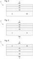
- the thin-film stack 15 comprises a substrate layer 150, a solid-state phase-switching layer 151 interposed between a transparent encapsulation layer 152 and a spacer layer 153 separating said phase-switching layer 151 from the substrate layer 150.
- the interference colors are generated by an interference effect produced by the arrangement of the encapsulation layer 152, the phase-switching layer 151, the spacer layer 153 and the substrate layer 150, in a reflective or transmissive manner depending on the exemplary embodiment of the present invention considered.
- the stack of thin layers 15 can be deposited on a support, made of any suitable material, said support being constituted by all or part of the covering component 14.
- the substrate layer 150 is arranged against the support and separates the spacing layer 153 from the support.
- the support can be made of metallic material, silicon with native oxide, glass, quartz, sapphire, polyethylene terephthalate, for example in the form of a film.
- the substrate layer 150 may be formed by a reflective layer, for example made by a metal mirror, preferably made of a material having a high reflection factor, for example platinum, rhodium, silver, aluminum, etc.
- This layer may have a thickness, defined here as being the dimension according to the direction in which the thin layers are superimposed on each other, of approximately 100 nm.
- the spacer layer 153 is made of transparent dielectric material. Such a material may be indium tin oxide, silicon dioxide or zinc sulfide. Preferably, the spacer layer 153 has a thickness of between 50 nm and 200 nm.
- the phase-switching layer 151 is configured to have two switchable phase states, preferably reversibly.
- the phase-switching layer 151 is configured to be able to pass, following exposure to light rays, from an initial crystalline or amorphous phase to a final amorphous or crystalline phase, respectively, and return to its initial phase.
- the exposure of the stack of thin layers 15 to the light rays locally generates a localized rise in temperature of the phase-switched layer 151.
- a temperature located above the glass transition point applied for a sufficiently long time, for example several seconds or tens of seconds induces a crystallization of the phase-switched layer 151, i.e. a change from the amorphous phase to the crystalline phase, and a temperature located above the melting point applied for a sufficiently short time to freeze the amorphous phase without recrystallization induces an amorphization of the phase-switched layer 151, i.e. a change from the crystalline phase to the amorphous phase.
- the phase-switched layer 151 has an amorphous phase after being deposited, such that the initial phase is the amorphous phase.
- the phase switching layer 151 does not have the same refractive index depending on whether it has a crystalline phase or an amorphous phase. Thus, the phase change of the phase switching layer 151 varies its refractive index, and therefore the perception of its visual appearance for a user to the extent that the interference color of the stack is dependent on the refractive index of the phase switching layer 151.
- the phase-switched layer 151 is configured so that its refractive index exhibits one of two values following exposure to the light rays. It should be noted that the light rays are generated so as to locally impact the stack of thin layers 15 from the encapsulation layer 152 so that the dressing component has two different interference colors.
- the light rays are preferably generated by a laser beam controlled by a control unit known per se to those skilled in the art, so as to control at least the localized rise in the temperature of the phase-switched layer 151, the exposure time and the shape of the predefined exposure zone 16 on the surface of the stack of thin layers 15.
- the laser beam emits light rays whose wavelength is in the infrared range
- the invention can also be implemented with lasers whose beam emits light rays whose wavelength is in the visible range or in the ultraviolet range.
- the working power of the laser is relatively low, preferably around 50 mW with a pulse duration of the order of 5 ms, i.e. a pulse energy of the order of 250 ⁇ J, in order to carry out the phase switching of the phase-switched layer 151 without risking damage to it by overheating, ablation, etc.
- the encapsulation layer 152 has a thickness of approximately 10 nm.
- the stack of thin layers 15 advantageously has a very low thickness and consequently can be applied to the exterior component 14 of the watch case 10 without modifying the design of said watch case 10 or said exterior component 14.
- the covering component 14 is in this case, for example, constituted by a glass or by a dial made of a transparent material.
- the stack of thin layers 15 is thus located in the internal volume of the watch case 10 and is not exposed to possible friction.
- the substrate layer 150 can be formed by the support, i.e. by the covering component 14, which is then made of reflective material, for example platinum, rhodium, silver, aluminum, etc.
- the substrate layer 150 is formed by a reflective layer, the stack of thin layers 15 is of a nature to reflect the light to which it is exposed, and to generate an aesthetic appearance of solid, opaque interference colors.
- the substrate 150 is not formed by a reflective layer, unlike the exemplary embodiments described previously and illustrated in the figures 2 to 4 , but is transparent or translucent. More specifically, the substrate layer 150 is formed by a transparent or translucent material, such as polyethylene terephthalate, glass, sapphire, etc.
- the interference effect produced by the arrangement of the phase-switching layer 151, the spacer layer 153 and the substrate layer 150 is of the transmissive type.
- the decoration generated by the stack of thin layers 15 can be observed by the user both through the encapsulation layer 152 and through the substrate layer 150.
- the covering component 14 can advantageously be constituted by a glass or a dial.
- the different thin layers of the stack of thin layers 15 can be deposited by a cathode sputtering method, or by any other suitable deposition method.
Landscapes
- Physics & Mathematics (AREA)
- General Physics & Mathematics (AREA)
- Engineering & Computer Science (AREA)
- Manufacturing & Machinery (AREA)
- Laminated Bodies (AREA)
- Surface Treatment Of Glass (AREA)
Claims (6)
- Uhrengehäuse (10), das einen Mittelteil (11), an dem ein Glas (12) und ein Boden (13) befestigt ist, umfasst, um ein Innenvolumen zu bilden, wobei das Uhrengehäuse (10) in dem Innenvolumen eine Verkleidungskomponente (14) beinhaltet, auf der ein Stapel aus Dünnschichten (15) aufgebracht ist, umfassend eine Substratschicht (150), eine Phasenumschaltschicht (151) im festen Zustand, die zwischen einer transparenten Einkapselungsschicht (152) und einer Abstandsschicht (153), welche die Phasenumschaltschicht (151) von der Substratschicht (150) trennt, eingesetzt ist, wobei die Phasenumschaltschicht (151) konfiguriert ist, um einen Brechungsindex aufzuweisen, der imstande ist, sich unter der Aussetzung von Lichtstrahlen zu verändern, um dem Stapel aus Dünnschichten (15) mindestens zwei Interferenzfarben zu verleihen, wobei die Substratschicht (150) durch eine reflektierende Schicht gebildet wird, wobei der Stapel aus Dünnschichten (15) auf einem Träger aufgebracht ist, der aus der gesamten Verkleidungskomponente (14) oder einem Teil davon besteht, wobei die Einkapselungsschicht (152) durch den Träger gebildet wird.
- Uhrengehäuse (10) nach Anspruch 1, wobei die Phasenumschaltschicht (151) konfiguriert ist, um zwei reversibel umschaltbare Phasenzustände aufzuweisen, wobei die Phasenzustände eine kristalline Phase und eine amorphe Phase sind.
- Uhrengehäuse (10) nach einem der Ansprüche 1 bis 2, wobei die Einkapselungsschicht (152) für die Wellenlänge der Lichtstrahlen transparent ist, unter deren Aussetzung der Brechungsindex der Phasenumschaltschicht (151) imstande ist, sich zu verändern.
- Uhrengehäuse (10) nach einem der Ansprüche 1 bis 3, wobei die Verkleidungskomponente (14) ein Zifferblatt, eine Struktur eines Uhrwerks (17), ein Glas, eine Anzeige, ein Zeiger, eine Applike, ein Logo oder eine Schwungmasse ist.
- Verfahren zum Verzieren der Verkleidungskomponente (14) eines Uhrengehäuses (10) nach einem der Ansprüche 1 bis 4, das darin besteht, den Stapel aus Dünnschichten (15) in einem vordefinierten Aussetzungsbereich (16) Lichtstrahlen auszusetzen, um die Phase der Phasenumschaltschicht (151) lokal zu ändern, und ein Motiv auf der Verkleidungskomponente (14) zu erzeugen.
- Verfahren zum Verzieren nach Anspruch 5, wobei die Lichtstrahlen durch ein Laserstrahlenbündel erzeugt werden, das von einer Steuereinheit angesteuert wird, um den lokalen Anstieg der Temperatur der Phasenumschaltschicht (151), die Aussetzungszeit und die Form des vordefinierten Aussetzungsbereichs (16) zu beherrschen.
Priority Applications (9)
| Application Number | Priority Date | Filing Date | Title |
|---|---|---|---|
| EP21209841.2A EP4184255B1 (de) | 2021-11-23 | 2021-11-23 | Armbanduhrengehäuse mit einer verkleidungskomponente, auf der ein stapel aus dünnschichten aufgebracht ist |
| EP22191469.0A EP4184256A1 (de) | 2021-11-23 | 2022-08-22 | Uhrengehäuse mit einer verkleidungskomponente, auf der ein dünnschichtstapel aufgelagert ist |
| US17/940,470 US20230161294A1 (en) | 2021-11-23 | 2022-09-08 | Watch case comprising an external part component whereon a stack of thin layers is deposited |
| US17/940,216 US20230161295A1 (en) | 2021-11-23 | 2022-09-08 | Watch case comprising an external part component whereon a stack of thin layers is deposited |
| JP2022143504A JP7559021B2 (ja) | 2021-11-23 | 2022-09-09 | 薄層の積層体が堆積されるドレッシングコンポーネントを備える携行型時計ケース |
| JP2022143503A JP7559020B2 (ja) | 2021-11-23 | 2022-09-09 | 薄層の積層体が堆積されるドレッシングコンポーネントを備える携行型時計ケース |
| CN202211472613.6A CN116149158A (zh) | 2021-11-23 | 2022-11-23 | 包括其上沉积有成堆薄层的外部构件的表壳 |
| CN202211473611.9A CN116149159A (zh) | 2021-11-23 | 2022-11-23 | 包括其上沉积有成堆薄层的外部构件的表壳 |
| JP2024112476A JP2024138491A (ja) | 2021-11-23 | 2024-07-12 | 薄層の積層体が堆積されるドレッシングコンポーネントを備える携行型時計ケース |
Applications Claiming Priority (1)
| Application Number | Priority Date | Filing Date | Title |
|---|---|---|---|
| EP21209841.2A EP4184255B1 (de) | 2021-11-23 | 2021-11-23 | Armbanduhrengehäuse mit einer verkleidungskomponente, auf der ein stapel aus dünnschichten aufgebracht ist |
Publications (2)
| Publication Number | Publication Date |
|---|---|
| EP4184255A1 EP4184255A1 (de) | 2023-05-24 |
| EP4184255B1 true EP4184255B1 (de) | 2025-04-16 |
Family
ID=78770439
Family Applications (2)
| Application Number | Title | Priority Date | Filing Date |
|---|---|---|---|
| EP21209841.2A Active EP4184255B1 (de) | 2021-11-23 | 2021-11-23 | Armbanduhrengehäuse mit einer verkleidungskomponente, auf der ein stapel aus dünnschichten aufgebracht ist |
| EP22191469.0A Pending EP4184256A1 (de) | 2021-11-23 | 2022-08-22 | Uhrengehäuse mit einer verkleidungskomponente, auf der ein dünnschichtstapel aufgelagert ist |
Family Applications After (1)
| Application Number | Title | Priority Date | Filing Date |
|---|---|---|---|
| EP22191469.0A Pending EP4184256A1 (de) | 2021-11-23 | 2022-08-22 | Uhrengehäuse mit einer verkleidungskomponente, auf der ein dünnschichtstapel aufgelagert ist |
Country Status (4)
| Country | Link |
|---|---|
| US (2) | US20230161295A1 (de) |
| EP (2) | EP4184255B1 (de) |
| JP (3) | JP7559020B2 (de) |
| CN (2) | CN116149159A (de) |
Families Citing this family (2)
| Publication number | Priority date | Publication date | Assignee | Title |
|---|---|---|---|---|
| EP4184255B1 (de) * | 2021-11-23 | 2025-04-16 | The Swatch Group Research and Development Ltd | Armbanduhrengehäuse mit einer verkleidungskomponente, auf der ein stapel aus dünnschichten aufgebracht ist |
| EP4575670A1 (de) * | 2023-12-20 | 2025-06-25 | The Swatch Group Research and Development Ltd | Verkleidungsbauteil mit einem substrat mit lokalen brechungsindexänderungen und verfahren zur herstellung eines solchen verkleidungsbauteils |
Citations (27)
| Publication number | Priority date | Publication date | Assignee | Title |
|---|---|---|---|---|
| CH531737A (fr) | 1969-10-14 | 1972-08-31 | Metalem Sa | Procédé de fabrication d'un cadran d'horlogerie muni d'au moins un cadran de compteur ou de petite seconde et cadran d'horlogerie obtenu par ce procédé |
| US3851460A (en) | 1972-08-14 | 1974-12-03 | Piquerez E Sa | Watch time display illumination |
| US5008869A (en) | 1990-04-11 | 1991-04-16 | Colony Corporation | Transparent dial face watch with replaceable visual display |
| JP2000155181A (ja) | 1998-11-24 | 2000-06-06 | Citizen Watch Co Ltd | 時計用文字板及びその製造方法 |
| EP1136698A1 (de) | 2000-03-17 | 2001-09-26 | Seiko Epson Corporation | Temperaturunterschiedantrieb und elektrische Vorrichtung, Uhrwerk und helles elektrisches Gerät mit diesem Antrieb |
| JP2003028049A (ja) | 2001-07-13 | 2003-01-29 | Seiko Epson Corp | エネルギ変換装置およびこれを備えた機器 |
| EP1331529A1 (de) | 2000-11-01 | 2003-07-30 | Kawaguchiko Seimitsu Company Limited | Zeitgeber-wähler und herstellungsverfahren dafür |
| EP1868046A1 (de) | 2005-03-30 | 2007-12-19 | Citizen Holdings Co., Ltd. | Instrumenten-indikationstafel und verfahren zur herstellung einer instrumenten-indikationstafel |
| US7499380B2 (en) | 2003-04-01 | 2009-03-03 | Artecad Sa | Dial |
| EP2420901B1 (de) | 2010-08-19 | 2014-05-21 | Seiko Epson Corporation | Uhrenziffernblatt, Verfahren zur Herstellung eines Uhrenziffernblatts, und eine Uhr |
| US8964513B2 (en) | 2005-06-14 | 2015-02-24 | The Swatch Group Research And Development Ltd | Technical or decorative piece associating a transparent material and a silicon based amorphous material and method of manufacturing the same |
| US20160336036A1 (en) | 2013-12-23 | 2016-11-17 | Isis Innovation Limited | Optical device |
| EP2593840B1 (de) | 2010-07-16 | 2017-11-15 | ETA SA Manufacture Horlogère Suisse | Verfahren zur einstellung der schwingungsfrequenz oder trägheit, und unruh einer unruh-federanordnung einer uhr |
| CN207037338U (zh) | 2017-05-31 | 2018-02-23 | 信利光电股份有限公司 | 一种新型手表表盘 |
| EP3087430B1 (de) | 2013-12-23 | 2018-05-02 | Oxford University Innovation Limited | Anzeigevorrichtung beruhend auf phasenwechselmaterialien |
| US20180203261A1 (en) | 2015-07-22 | 2018-07-19 | Oxford University Innovation Limited | Optical device |
| WO2018185461A1 (en) | 2017-04-06 | 2018-10-11 | Bodle Technologies Ltd | Optical apparatus |
| CN208673057U (zh) | 2018-08-24 | 2019-03-29 | 信利光电股份有限公司 | 一种手表 |
| CN208888589U (zh) | 2018-08-24 | 2019-05-21 | 信利光电股份有限公司 | 一种可切换表盘字体颜色的手表 |
| EP3588203A1 (de) | 2018-06-25 | 2020-01-01 | Rolex Sa | Vielseitig einsetzbare uhrenkomponente |
| CN209895141U (zh) | 2019-03-26 | 2020-01-03 | 信利光电股份有限公司 | 一种表盘及手表 |
| EP3386337B1 (de) | 2015-12-09 | 2020-02-05 | The Swatch Group Research and Development Ltd. | Bekleidungselement in variablen farben |
| EP3640746A1 (de) | 2018-10-11 | 2020-04-22 | Giesecke+Devrient Currency Technology GmbH | Ziffernblatt für eine uhr |
| WO2020128487A1 (en) | 2018-12-21 | 2020-06-25 | Bodle Technologies Limited | Display material |
| EP3789830A1 (de) | 2019-09-09 | 2021-03-10 | The Swatch Group Research and Development Ltd | Zifferblatt und herstellungsverfahren eines zifferblatts für eine armbanduhr |
| EP3835452A1 (de) | 2019-12-09 | 2021-06-16 | The Swatch Group Research and Development Ltd | Herstellungsverfahren einer dekoroberfläche |
| EP3483668B1 (de) | 2017-11-13 | 2022-11-02 | Rolex Sa | Befestigungssystem eines uhrwerks in einem armbanduhrengehäuse |
Family Cites Families (10)
| Publication number | Priority date | Publication date | Assignee | Title |
|---|---|---|---|---|
| EP1734018A1 (de) * | 2005-06-14 | 2006-12-20 | Comadur S.A. | Technisches oder dekoratives Element , wobei transparenten und amorphen Materialen verbunden werden, und Erstellungsverfahren dafür |
| US20100225989A1 (en) * | 2009-03-05 | 2010-09-09 | The Regents Of The University Of California | Phase change device |
| EP3226084B1 (de) * | 2016-03-29 | 2021-01-13 | The Swatch Group Research and Development Ltd. | Farbige uhrenkomponente |
| EP3339983B1 (de) * | 2016-12-23 | 2020-07-01 | The Swatch Group Research and Development Ltd | Perlmuttsubstrat, das mit einer gelben schicht beschichtet ist |
| JP6814054B2 (ja) * | 2017-01-23 | 2021-01-13 | シチズン時計株式会社 | 表示板 |
| EP3696151A1 (de) * | 2019-02-18 | 2020-08-19 | Rolex Sa | Farbiges armbanduhrenglas |
| JP7193370B2 (ja) * | 2019-02-18 | 2022-12-20 | シチズン時計株式会社 | 表示板とこの表示板を備えた時計 |
| JP7295009B2 (ja) * | 2019-02-26 | 2023-06-20 | シチズン時計株式会社 | 表示板及びこの表示板を用いた時計 |
| EP4733861A2 (de) * | 2019-09-23 | 2026-04-29 | The Swatch Group Research and Development Ltd | Uhrelement |
| EP4184255B1 (de) * | 2021-11-23 | 2025-04-16 | The Swatch Group Research and Development Ltd | Armbanduhrengehäuse mit einer verkleidungskomponente, auf der ein stapel aus dünnschichten aufgebracht ist |
-
2021
- 2021-11-23 EP EP21209841.2A patent/EP4184255B1/de active Active
-
2022
- 2022-08-22 EP EP22191469.0A patent/EP4184256A1/de active Pending
- 2022-09-08 US US17/940,216 patent/US20230161295A1/en active Pending
- 2022-09-08 US US17/940,470 patent/US20230161294A1/en active Pending
- 2022-09-09 JP JP2022143503A patent/JP7559020B2/ja active Active
- 2022-09-09 JP JP2022143504A patent/JP7559021B2/ja active Active
- 2022-11-23 CN CN202211473611.9A patent/CN116149159A/zh active Pending
- 2022-11-23 CN CN202211472613.6A patent/CN116149158A/zh active Pending
-
2024
- 2024-07-12 JP JP2024112476A patent/JP2024138491A/ja active Pending
Patent Citations (27)
| Publication number | Priority date | Publication date | Assignee | Title |
|---|---|---|---|---|
| CH531737A (fr) | 1969-10-14 | 1972-08-31 | Metalem Sa | Procédé de fabrication d'un cadran d'horlogerie muni d'au moins un cadran de compteur ou de petite seconde et cadran d'horlogerie obtenu par ce procédé |
| US3851460A (en) | 1972-08-14 | 1974-12-03 | Piquerez E Sa | Watch time display illumination |
| US5008869A (en) | 1990-04-11 | 1991-04-16 | Colony Corporation | Transparent dial face watch with replaceable visual display |
| JP2000155181A (ja) | 1998-11-24 | 2000-06-06 | Citizen Watch Co Ltd | 時計用文字板及びその製造方法 |
| EP1136698A1 (de) | 2000-03-17 | 2001-09-26 | Seiko Epson Corporation | Temperaturunterschiedantrieb und elektrische Vorrichtung, Uhrwerk und helles elektrisches Gerät mit diesem Antrieb |
| EP1331529A1 (de) | 2000-11-01 | 2003-07-30 | Kawaguchiko Seimitsu Company Limited | Zeitgeber-wähler und herstellungsverfahren dafür |
| JP2003028049A (ja) | 2001-07-13 | 2003-01-29 | Seiko Epson Corp | エネルギ変換装置およびこれを備えた機器 |
| US7499380B2 (en) | 2003-04-01 | 2009-03-03 | Artecad Sa | Dial |
| EP1868046A1 (de) | 2005-03-30 | 2007-12-19 | Citizen Holdings Co., Ltd. | Instrumenten-indikationstafel und verfahren zur herstellung einer instrumenten-indikationstafel |
| US8964513B2 (en) | 2005-06-14 | 2015-02-24 | The Swatch Group Research And Development Ltd | Technical or decorative piece associating a transparent material and a silicon based amorphous material and method of manufacturing the same |
| EP2593840B1 (de) | 2010-07-16 | 2017-11-15 | ETA SA Manufacture Horlogère Suisse | Verfahren zur einstellung der schwingungsfrequenz oder trägheit, und unruh einer unruh-federanordnung einer uhr |
| EP2420901B1 (de) | 2010-08-19 | 2014-05-21 | Seiko Epson Corporation | Uhrenziffernblatt, Verfahren zur Herstellung eines Uhrenziffernblatts, und eine Uhr |
| US20160336036A1 (en) | 2013-12-23 | 2016-11-17 | Isis Innovation Limited | Optical device |
| EP3087430B1 (de) | 2013-12-23 | 2018-05-02 | Oxford University Innovation Limited | Anzeigevorrichtung beruhend auf phasenwechselmaterialien |
| US20180203261A1 (en) | 2015-07-22 | 2018-07-19 | Oxford University Innovation Limited | Optical device |
| EP3386337B1 (de) | 2015-12-09 | 2020-02-05 | The Swatch Group Research and Development Ltd. | Bekleidungselement in variablen farben |
| WO2018185461A1 (en) | 2017-04-06 | 2018-10-11 | Bodle Technologies Ltd | Optical apparatus |
| CN207037338U (zh) | 2017-05-31 | 2018-02-23 | 信利光电股份有限公司 | 一种新型手表表盘 |
| EP3483668B1 (de) | 2017-11-13 | 2022-11-02 | Rolex Sa | Befestigungssystem eines uhrwerks in einem armbanduhrengehäuse |
| EP3588203A1 (de) | 2018-06-25 | 2020-01-01 | Rolex Sa | Vielseitig einsetzbare uhrenkomponente |
| CN208888589U (zh) | 2018-08-24 | 2019-05-21 | 信利光电股份有限公司 | 一种可切换表盘字体颜色的手表 |
| CN208673057U (zh) | 2018-08-24 | 2019-03-29 | 信利光电股份有限公司 | 一种手表 |
| EP3640746A1 (de) | 2018-10-11 | 2020-04-22 | Giesecke+Devrient Currency Technology GmbH | Ziffernblatt für eine uhr |
| WO2020128487A1 (en) | 2018-12-21 | 2020-06-25 | Bodle Technologies Limited | Display material |
| CN209895141U (zh) | 2019-03-26 | 2020-01-03 | 信利光电股份有限公司 | 一种表盘及手表 |
| EP3789830A1 (de) | 2019-09-09 | 2021-03-10 | The Swatch Group Research and Development Ltd | Zifferblatt und herstellungsverfahren eines zifferblatts für eine armbanduhr |
| EP3835452A1 (de) | 2019-12-09 | 2021-06-16 | The Swatch Group Research and Development Ltd | Herstellungsverfahren einer dekoroberfläche |
Non-Patent Citations (9)
| Title |
|---|
| ANONYMOUS: "Bodle entwickelt erstes SRD-Display", INVIDIS, 9 August 2020 (2020-08-09), XP093360313, Retrieved from the Internet <URL:https://invidis.de/2020/08/extrem-niedriger-stromverbrauch-bodle-entwickelt-erstes-srd-display/> |
| BELLO PEREZ YESSI: "Oxford-based Bodle gets £6m to launch new digital display tech", TECH CITY NEWS LIMITED T/A UKTN, 31 January 2018 (2018-01-31), XP093360317, Retrieved from the Internet <URL:https://www.uktech.news/tech-hubs/south-east/oxford/oxford-university-spinout-bodle-raises-6m-to-launch-new-digital-display-tech-20180131> |
| D14 - KELLY RAND: "How to: Upcycle an Old CD into a Clock", CRAFTING A GREEN WORLD, 6 August 2011 (2011-08-06), XP093360315 |
| HOSSEINI P.; WRIGHT C.D; BHASKARAN H.: "An optoelectronic framework enabled by low-dimensional phase-change films", NATURE, vol. 511, 10 July 2014 (2014-07-10), pages 206 - 211, XP002783103, DOI: 10.1038/nature13487 |
| INVENTOR VAMSI: "How to make amazing CD clock DIY craft at home", 24 November 2019 (2019-11-24), XP093360322, Retrieved from the Internet <URL:https://www.youtube.com/watch?v=Mjptw8wAZvI> |
| MERKX EVERT, BANDHU LOKESHWAR, KESHKAR SMRITI, NORTON JOHN, LAI LUC, TSAI ALBERT, PAUZA ANDREW, BHASKARAN HARISH, HOSSEINI PEIMAN: "Personnalisation de composants de montre utilisant un nouveau procédé de revêtement (PVD) interchangeable", BULLETIN SSC - SOCIÉTÉ SUISSE DE CHRONOMÉTRIE, vol. 92, 6 December 2021 (2021-12-06), pages 57 - 62, XP093360319 |
| MERTENS RON: "Meet SRD: Bodle's e-paper display technology based on PCM materials", E-INK-INFO, 21 December 2017 (2017-12-21), XP093360306, Retrieved from the Internet <URL:https://www.e-ink-info.com/meet-srd-bodles-e-paper-display-technology-based-pcm-materials> |
| TALAGRAND CLEMENT, TRIGGS GRAHAM, BANDHU LOKESHWAR, GARCIA‐CASTILLO SERGIO, BROUGHTON BEN, BHASKARAN HARISH, HOSSEINI PEIMAN: "Solid‐state reflective displays (SRD ) for video‐rate, full color, outdoor readable displays", JOURNAL OF THE SOCIETY FOR INFORMATION DISPLAY - SID, SOCIETY FOR INFORMATION DISPLAY., US, vol. 26, no. 10, 1 October 2018 (2018-10-01), US , pages 619 - 624, XP093360309, ISSN: 1071-0922, DOI: 10.1002/jsid.732 |
| TEDX TALKS: "Reflecting on Displays - the future of colour Harish Bhaskaran TEDxEton", 5 June 2017 (2017-06-05), XP093360320, Retrieved from the Internet <URL:https://www.youtube.com/watch?v=Y3oBBMxX-u8&list=PPSV> |
Also Published As
| Publication number | Publication date |
|---|---|
| EP4184256A1 (de) | 2023-05-24 |
| CN116149158A (zh) | 2023-05-23 |
| JP2023076800A (ja) | 2023-06-02 |
| CN116149159A (zh) | 2023-05-23 |
| JP7559021B2 (ja) | 2024-10-01 |
| JP2023076801A (ja) | 2023-06-02 |
| EP4184255A1 (de) | 2023-05-24 |
| US20230161295A1 (en) | 2023-05-25 |
| JP7559020B2 (ja) | 2024-10-01 |
| US20230161294A1 (en) | 2023-05-25 |
| JP2024138491A (ja) | 2024-10-08 |
Similar Documents
| Publication | Publication Date | Title |
|---|---|---|
| EP1893542B1 (de) | Technisches oder dekoratives teil mit einer kombination aus einem transparenten material und einem auf siliciumdioxid basierenden amorphen material und herstellungsverfahren dafür | |
| EP4184255B1 (de) | Armbanduhrengehäuse mit einer verkleidungskomponente, auf der ein stapel aus dünnschichten aufgebracht ist | |
| EP0786685B1 (de) | Verzierung anzeigende Vorrichtung und diese enthaltende Uhr | |
| EP4170435A1 (de) | Verfahren zur herstellung eines verkleidungsteils, insbesondere eines verkleidungsteils für uhren | |
| EP3896193A1 (de) | Uhrenkomponente mit einem verbesserten optischen interferenzsystem | |
| EP3588203A1 (de) | Vielseitig einsetzbare uhrenkomponente | |
| EP3896192A1 (de) | Uhrenkomponente mit einem verbesserten optischen interferenzsystem, die eine schicht auf zinkbasis umfasst | |
| EP3896191A1 (de) | Uhrenkomponente mit einem verbesserten optischen interferenzsystem, die eine schicht auf nickelbasis umfasst | |
| EP3696151A1 (de) | Farbiges armbanduhrenglas | |
| CH719162A2 (fr) | Boîte de montre comprenant un composant d'habillage sur lequel est déposé un empilement de couches minces. | |
| EP4060386A1 (de) | Verkleidungsteil einer uhr oder eines schmuckstücks mit einer interferenzfarbbeschichtung und verfahren zur herstellung dieses teils | |
| CH718465A2 (fr) | Procédé de fabrication d'une pièce d'habillage d'horlogerie ou de bijouterie à base ceramique et à decor structuré. | |
| EP3764167B1 (de) | Verfahren zum erhalten einer uhrenkomponente, deren oberfläche zumindest zum teil mit einer farbschicht beschichtet ist | |
| EP4224258A1 (de) | Komponente zur verkleidung einer uhr oder eines schmuck- oder juwelierartikels und verfahren zur herstellung einer solchen verkleidungskomponente | |
| CH719085A2 (fr) | Procédé de fabrication d'une pièce d'habillage, notamment d'une pièce d'horlogerie. | |
| EP4060426B1 (de) | Verfahren zur herstellung eines verkleidungsteils einer uhr oder eines schmuckstücks auf keramikbasis und mit einem strukturierten dekor | |
| CH720373A2 (fr) | Procédé de fabrication d'un composant d'habillage transparent d'une montre, d'un article de mode ou d'un article de bijouterie ou de joaillerie | |
| HK40093851A (zh) | 包括其上沉积有成堆薄层的外部构件的表壳 | |
| HK40093853A (zh) | 包括其上沉积有成堆薄层的外部构件的表壳 | |
| CH719394A2 (fr) | Composant d'habillage pour une montre ou un article de bijouterie ou de joaillerie et procédé de fabrication d'un tel composant d'habillage | |
| EP1734018A1 (de) | Technisches oder dekoratives Element , wobei transparenten und amorphen Materialen verbunden werden, und Erstellungsverfahren dafür | |
| EP4524288A1 (de) | Verfahren zum dekorieren eines substrats durch auftragen einer maskenschicht auf sol-gel-basis zur herstellung eines verkleidungsteils | |
| EP4575670A1 (de) | Verkleidungsbauteil mit einem substrat mit lokalen brechungsindexänderungen und verfahren zur herstellung eines solchen verkleidungsbauteils | |
| CH721435A2 (fr) | Composant d'habillage comprenant un substrat dont la face d'habillage présente des couleurs interférentielles | |
| CH721050A2 (fr) | Procédé de décoration en trois dimensions d'un substrat afin de réaliser une pièce d'habillage |
Legal Events
| Date | Code | Title | Description |
|---|---|---|---|
| PUAI | Public reference made under article 153(3) epc to a published international application that has entered the european phase |
Free format text: ORIGINAL CODE: 0009012 |
|
| STAA | Information on the status of an ep patent application or granted ep patent |
Free format text: STATUS: THE APPLICATION HAS BEEN PUBLISHED |
|
| AK | Designated contracting states |
Kind code of ref document: A1 Designated state(s): AL AT BE BG CH CY CZ DE DK EE ES FI FR GB GR HR HU IE IS IT LI LT LU LV MC MK MT NL NO PL PT RO RS SE SI SK SM TR |
|
| P01 | Opt-out of the competence of the unified patent court (upc) registered |
Effective date: 20230615 |
|
| STAA | Information on the status of an ep patent application or granted ep patent |
Free format text: STATUS: REQUEST FOR EXAMINATION WAS MADE |
|
| 17P | Request for examination filed |
Effective date: 20231124 |
|
| RBV | Designated contracting states (corrected) |
Designated state(s): AL AT BE BG CH CY CZ DE DK EE ES FI FR GB GR HR HU IE IS IT LI LT LU LV MC MK MT NL NO PL PT RO RS SE SI SK SM TR |
|
| GRAP | Despatch of communication of intention to grant a patent |
Free format text: ORIGINAL CODE: EPIDOSNIGR1 |
|
| STAA | Information on the status of an ep patent application or granted ep patent |
Free format text: STATUS: GRANT OF PATENT IS INTENDED |
|
| RIC1 | Information provided on ipc code assigned before grant |
Ipc: G02B 5/28 20060101ALN20250109BHEP Ipc: G02F 1/01 20060101ALN20250109BHEP Ipc: G02F 1/00 20060101ALN20250109BHEP Ipc: G04B 39/00 20060101ALI20250109BHEP Ipc: G04B 19/12 20060101ALI20250109BHEP Ipc: G04B 45/00 20060101AFI20250109BHEP |
|
| INTG | Intention to grant announced |
Effective date: 20250127 |
|
| RIC1 | Information provided on ipc code assigned before grant |
Ipc: G02B 5/28 20060101ALN20250117BHEP Ipc: G02F 1/01 20060101ALN20250117BHEP Ipc: G02F 1/00 20060101ALN20250117BHEP Ipc: G04B 39/00 20060101ALI20250117BHEP Ipc: G04B 19/12 20060101ALI20250117BHEP Ipc: G04B 45/00 20060101AFI20250117BHEP |
|
| GRAS | Grant fee paid |
Free format text: ORIGINAL CODE: EPIDOSNIGR3 |
|
| GRAA | (expected) grant |
Free format text: ORIGINAL CODE: 0009210 |
|
| STAA | Information on the status of an ep patent application or granted ep patent |
Free format text: STATUS: THE PATENT HAS BEEN GRANTED |
|
| AK | Designated contracting states |
Kind code of ref document: B1 Designated state(s): AL AT BE BG CH CY CZ DE DK EE ES FI FR GB GR HR HU IE IS IT LI LT LU LV MC MK MT NL NO PL PT RO RS SE SI SK SM TR |
|
| REG | Reference to a national code |
Ref country code: GB Ref legal event code: FG4D Free format text: NOT ENGLISH |
|
| REG | Reference to a national code |
Ref country code: CH Ref legal event code: EP Ref country code: DE Ref legal event code: R096 Ref document number: 602021029179 Country of ref document: DE |
|
| REG | Reference to a national code |
Ref country code: IE Ref legal event code: FG4D Free format text: LANGUAGE OF EP DOCUMENT: FRENCH |
|
| REG | Reference to a national code |
Ref country code: NL Ref legal event code: MP Effective date: 20250416 |
|
| PG25 | Lapsed in a contracting state [announced via postgrant information from national office to epo] |
Ref country code: NL Free format text: LAPSE BECAUSE OF FAILURE TO SUBMIT A TRANSLATION OF THE DESCRIPTION OR TO PAY THE FEE WITHIN THE PRESCRIBED TIME-LIMIT Effective date: 20250416 |
|
| REG | Reference to a national code |
Ref country code: AT Ref legal event code: MK05 Ref document number: 1786150 Country of ref document: AT Kind code of ref document: T Effective date: 20250416 |
|
| PG25 | Lapsed in a contracting state [announced via postgrant information from national office to epo] |
Ref country code: FI Free format text: LAPSE BECAUSE OF FAILURE TO SUBMIT A TRANSLATION OF THE DESCRIPTION OR TO PAY THE FEE WITHIN THE PRESCRIBED TIME-LIMIT Effective date: 20250416 Ref country code: ES Free format text: LAPSE BECAUSE OF FAILURE TO SUBMIT A TRANSLATION OF THE DESCRIPTION OR TO PAY THE FEE WITHIN THE PRESCRIBED TIME-LIMIT Effective date: 20250416 Ref country code: PT Free format text: LAPSE BECAUSE OF FAILURE TO SUBMIT A TRANSLATION OF THE DESCRIPTION OR TO PAY THE FEE WITHIN THE PRESCRIBED TIME-LIMIT Effective date: 20250818 |
|
| REG | Reference to a national code |
Ref country code: LT Ref legal event code: MG9D |
|
| PG25 | Lapsed in a contracting state [announced via postgrant information from national office to epo] |
Ref country code: GR Free format text: LAPSE BECAUSE OF FAILURE TO SUBMIT A TRANSLATION OF THE DESCRIPTION OR TO PAY THE FEE WITHIN THE PRESCRIBED TIME-LIMIT Effective date: 20250717 Ref country code: NO Free format text: LAPSE BECAUSE OF FAILURE TO SUBMIT A TRANSLATION OF THE DESCRIPTION OR TO PAY THE FEE WITHIN THE PRESCRIBED TIME-LIMIT Effective date: 20250716 |
|
| PG25 | Lapsed in a contracting state [announced via postgrant information from national office to epo] |
Ref country code: PL Free format text: LAPSE BECAUSE OF FAILURE TO SUBMIT A TRANSLATION OF THE DESCRIPTION OR TO PAY THE FEE WITHIN THE PRESCRIBED TIME-LIMIT Effective date: 20250416 |
|
| PG25 | Lapsed in a contracting state [announced via postgrant information from national office to epo] |
Ref country code: BG Free format text: LAPSE BECAUSE OF FAILURE TO SUBMIT A TRANSLATION OF THE DESCRIPTION OR TO PAY THE FEE WITHIN THE PRESCRIBED TIME-LIMIT Effective date: 20250416 |
|
| PG25 | Lapsed in a contracting state [announced via postgrant information from national office to epo] |
Ref country code: HR Free format text: LAPSE BECAUSE OF FAILURE TO SUBMIT A TRANSLATION OF THE DESCRIPTION OR TO PAY THE FEE WITHIN THE PRESCRIBED TIME-LIMIT Effective date: 20250416 |
|
| PG25 | Lapsed in a contracting state [announced via postgrant information from national office to epo] |
Ref country code: AT Free format text: LAPSE BECAUSE OF FAILURE TO SUBMIT A TRANSLATION OF THE DESCRIPTION OR TO PAY THE FEE WITHIN THE PRESCRIBED TIME-LIMIT Effective date: 20250416 |
|
| PG25 | Lapsed in a contracting state [announced via postgrant information from national office to epo] |
Ref country code: RS Free format text: LAPSE BECAUSE OF FAILURE TO SUBMIT A TRANSLATION OF THE DESCRIPTION OR TO PAY THE FEE WITHIN THE PRESCRIBED TIME-LIMIT Effective date: 20250716 |
|
| PG25 | Lapsed in a contracting state [announced via postgrant information from national office to epo] |
Ref country code: IS Free format text: LAPSE BECAUSE OF FAILURE TO SUBMIT A TRANSLATION OF THE DESCRIPTION OR TO PAY THE FEE WITHIN THE PRESCRIBED TIME-LIMIT Effective date: 20250816 |
|
| PG25 | Lapsed in a contracting state [announced via postgrant information from national office to epo] |
Ref country code: LV Free format text: LAPSE BECAUSE OF FAILURE TO SUBMIT A TRANSLATION OF THE DESCRIPTION OR TO PAY THE FEE WITHIN THE PRESCRIBED TIME-LIMIT Effective date: 20250416 |
|
| REG | Reference to a national code |
Ref country code: CH Ref legal event code: U11 Free format text: ST27 STATUS EVENT CODE: U-0-0-U10-U11 (AS PROVIDED BY THE NATIONAL OFFICE) Effective date: 20251201 |
|
| PGFP | Annual fee paid to national office [announced via postgrant information from national office to epo] |
Ref country code: DE Payment date: 20251022 Year of fee payment: 5 |
|
| PG25 | Lapsed in a contracting state [announced via postgrant information from national office to epo] |
Ref country code: SM Free format text: LAPSE BECAUSE OF FAILURE TO SUBMIT A TRANSLATION OF THE DESCRIPTION OR TO PAY THE FEE WITHIN THE PRESCRIBED TIME-LIMIT Effective date: 20250416 Ref country code: DK Free format text: LAPSE BECAUSE OF FAILURE TO SUBMIT A TRANSLATION OF THE DESCRIPTION OR TO PAY THE FEE WITHIN THE PRESCRIBED TIME-LIMIT Effective date: 20250416 |
|
| PGFP | Annual fee paid to national office [announced via postgrant information from national office to epo] |
Ref country code: FR Payment date: 20251022 Year of fee payment: 5 |
|
| REG | Reference to a national code |
Ref country code: DE Ref legal event code: R026 Ref document number: 602021029179 Country of ref document: DE |
|
| PGFP | Annual fee paid to national office [announced via postgrant information from national office to epo] |
Ref country code: CH Payment date: 20251201 Year of fee payment: 5 |
|
| PG25 | Lapsed in a contracting state [announced via postgrant information from national office to epo] |
Ref country code: CZ Free format text: LAPSE BECAUSE OF FAILURE TO SUBMIT A TRANSLATION OF THE DESCRIPTION OR TO PAY THE FEE WITHIN THE PRESCRIBED TIME-LIMIT Effective date: 20250416 |
|
| PLBI | Opposition filed |
Free format text: ORIGINAL CODE: 0009260 |
|
| PG25 | Lapsed in a contracting state [announced via postgrant information from national office to epo] |
Ref country code: EE Free format text: LAPSE BECAUSE OF FAILURE TO SUBMIT A TRANSLATION OF THE DESCRIPTION OR TO PAY THE FEE WITHIN THE PRESCRIBED TIME-LIMIT Effective date: 20250416 |
|
| PG25 | Lapsed in a contracting state [announced via postgrant information from national office to epo] |
Ref country code: SK Free format text: LAPSE BECAUSE OF FAILURE TO SUBMIT A TRANSLATION OF THE DESCRIPTION OR TO PAY THE FEE WITHIN THE PRESCRIBED TIME-LIMIT Effective date: 20250416 |
|
| PG25 | Lapsed in a contracting state [announced via postgrant information from national office to epo] |
Ref country code: IT Free format text: LAPSE BECAUSE OF FAILURE TO SUBMIT A TRANSLATION OF THE DESCRIPTION OR TO PAY THE FEE WITHIN THE PRESCRIBED TIME-LIMIT Effective date: 20250416 |
|
| REG | Reference to a national code |
Ref country code: CH Ref legal event code: L10 Free format text: ST27 STATUS EVENT CODE: U-0-0-L10-L00 (AS PROVIDED BY THE NATIONAL OFFICE) Effective date: 20260128 |
|
| PLAX | Notice of opposition and request to file observation + time limit sent |
Free format text: ORIGINAL CODE: EPIDOSNOBS2 |
|
| 26 | Opposition filed |
Opponent name: KRAUS & LEDERER PARTGMBB Effective date: 20260116 |
|
| PG25 | Lapsed in a contracting state [announced via postgrant information from national office to epo] |
Ref country code: RO Free format text: LAPSE BECAUSE OF FAILURE TO SUBMIT A TRANSLATION OF THE DESCRIPTION OR TO PAY THE FEE WITHIN THE PRESCRIBED TIME-LIMIT Effective date: 20250416 |