EP4190764A1 - Verbindungskörper, schaltungssubstrat, halbleiterbauelement und verfahren zur herstellung eines verbindungskörpers - Google Patents
Verbindungskörper, schaltungssubstrat, halbleiterbauelement und verfahren zur herstellung eines verbindungskörpers Download PDFInfo
- Publication number
- EP4190764A1 EP4190764A1 EP21850137.7A EP21850137A EP4190764A1 EP 4190764 A1 EP4190764 A1 EP 4190764A1 EP 21850137 A EP21850137 A EP 21850137A EP 4190764 A1 EP4190764 A1 EP 4190764A1
- Authority
- EP
- European Patent Office
- Prior art keywords
- copper plate
- bonding
- less
- region
- ceramic substrate
- Prior art date
- Legal status (The legal status is an assumption and is not a legal conclusion. Google has not performed a legal analysis and makes no representation as to the accuracy of the status listed.)
- Pending
Links
Images

Classifications
-
- C—CHEMISTRY; METALLURGY
- C04—CEMENTS; CONCRETE; ARTIFICIAL STONE; CERAMICS; REFRACTORIES
- C04B—LIME, MAGNESIA; SLAG; CEMENTS; COMPOSITIONS THEREOF, e.g. MORTARS, CONCRETE OR LIKE BUILDING MATERIALS; ARTIFICIAL STONE; CERAMICS; REFRACTORIES; TREATMENT OF NATURAL STONE
- C04B37/00—Joining burned ceramic articles with other burned ceramic articles or other articles by heating
- C04B37/02—Joining burned ceramic articles with other burned ceramic articles or other articles by heating with metallic articles
- C04B37/023—Joining burned ceramic articles with other burned ceramic articles or other articles by heating with metallic articles characterised by the interlayer used
- C04B37/026—Joining burned ceramic articles with other burned ceramic articles or other articles by heating with metallic articles characterised by the interlayer used consisting of metals or metal salts
-
- H—ELECTRICITY
- H10—SEMICONDUCTOR DEVICES; ELECTRIC SOLID-STATE DEVICES NOT OTHERWISE PROVIDED FOR
- H10W—GENERIC PACKAGES, INTERCONNECTIONS, CONNECTORS OR OTHER CONSTRUCTIONAL DETAILS OF DEVICES COVERED BY CLASS H10
- H10W70/00—Package substrates; Interposers; Redistribution layers [RDL]
- H10W70/60—Insulating or insulated package substrates; Interposers; Redistribution layers
- H10W70/67—Insulating or insulated package substrates; Interposers; Redistribution layers characterised by their insulating layers or insulating parts
- H10W70/69—Insulating materials thereof
-
- B—PERFORMING OPERATIONS; TRANSPORTING
- B23—MACHINE TOOLS; METAL-WORKING NOT OTHERWISE PROVIDED FOR
- B23K—SOLDERING OR UNSOLDERING; WELDING; CLADDING OR PLATING BY SOLDERING OR WELDING; CUTTING BY APPLYING HEAT LOCALLY, e.g. FLAME CUTTING; WORKING BY LASER BEAM
- B23K35/00—Rods, electrodes, materials, or media, for use in soldering, welding, or cutting
- B23K35/22—Rods, electrodes, materials, or media, for use in soldering, welding, or cutting characterised by the composition or nature of the material
- B23K35/24—Selection of soldering or welding materials proper
- B23K35/30—Selection of soldering or welding materials proper with the principal constituent melting at less than 1550°C
- B23K35/302—Cu as the principal constituent
-
- C—CHEMISTRY; METALLURGY
- C04—CEMENTS; CONCRETE; ARTIFICIAL STONE; CERAMICS; REFRACTORIES
- C04B—LIME, MAGNESIA; SLAG; CEMENTS; COMPOSITIONS THEREOF, e.g. MORTARS, CONCRETE OR LIKE BUILDING MATERIALS; ARTIFICIAL STONE; CERAMICS; REFRACTORIES; TREATMENT OF NATURAL STONE
- C04B37/00—Joining burned ceramic articles with other burned ceramic articles or other articles by heating
- C04B37/02—Joining burned ceramic articles with other burned ceramic articles or other articles by heating with metallic articles
- C04B37/023—Joining burned ceramic articles with other burned ceramic articles or other articles by heating with metallic articles characterised by the interlayer used
-
- C—CHEMISTRY; METALLURGY
- C04—CEMENTS; CONCRETE; ARTIFICIAL STONE; CERAMICS; REFRACTORIES
- C04B—LIME, MAGNESIA; SLAG; CEMENTS; COMPOSITIONS THEREOF, e.g. MORTARS, CONCRETE OR LIKE BUILDING MATERIALS; ARTIFICIAL STONE; CERAMICS; REFRACTORIES; TREATMENT OF NATURAL STONE
- C04B37/00—Joining burned ceramic articles with other burned ceramic articles or other articles by heating
- C04B37/02—Joining burned ceramic articles with other burned ceramic articles or other articles by heating with metallic articles
- C04B37/023—Joining burned ceramic articles with other burned ceramic articles or other articles by heating with metallic articles characterised by the interlayer used
- C04B37/025—Joining burned ceramic articles with other burned ceramic articles or other articles by heating with metallic articles characterised by the interlayer used consisting of glass or ceramic material
-
- H—ELECTRICITY
- H05—ELECTRIC TECHNIQUES NOT OTHERWISE PROVIDED FOR
- H05K—PRINTED CIRCUITS; CASINGS OR CONSTRUCTIONAL DETAILS OF ELECTRIC APPARATUS; MANUFACTURE OF ASSEMBLAGES OF ELECTRICAL COMPONENTS
- H05K1/00—Printed circuits
- H05K1/02—Details
- H05K1/03—Use of materials for the substrate
-
- H—ELECTRICITY
- H05—ELECTRIC TECHNIQUES NOT OTHERWISE PROVIDED FOR
- H05K—PRINTED CIRCUITS; CASINGS OR CONSTRUCTIONAL DETAILS OF ELECTRIC APPARATUS; MANUFACTURE OF ASSEMBLAGES OF ELECTRICAL COMPONENTS
- H05K1/00—Printed circuits
- H05K1/02—Details
- H05K1/03—Use of materials for the substrate
- H05K1/0306—Inorganic insulating substrates, e.g. ceramic, glass
-
- H—ELECTRICITY
- H05—ELECTRIC TECHNIQUES NOT OTHERWISE PROVIDED FOR
- H05K—PRINTED CIRCUITS; CASINGS OR CONSTRUCTIONAL DETAILS OF ELECTRIC APPARATUS; MANUFACTURE OF ASSEMBLAGES OF ELECTRICAL COMPONENTS
- H05K3/00—Apparatus or processes for manufacturing printed circuits
- H05K3/38—Improvement of the adhesion between the insulating substrate and the metal
-
- H—ELECTRICITY
- H05—ELECTRIC TECHNIQUES NOT OTHERWISE PROVIDED FOR
- H05K—PRINTED CIRCUITS; CASINGS OR CONSTRUCTIONAL DETAILS OF ELECTRIC APPARATUS; MANUFACTURE OF ASSEMBLAGES OF ELECTRICAL COMPONENTS
- H05K3/00—Apparatus or processes for manufacturing printed circuits
- H05K3/38—Improvement of the adhesion between the insulating substrate and the metal
- H05K3/388—Improvement of the adhesion between the insulating substrate and the metal by the use of a metallic or inorganic thin film adhesion layer
-
- H—ELECTRICITY
- H10—SEMICONDUCTOR DEVICES; ELECTRIC SOLID-STATE DEVICES NOT OTHERWISE PROVIDED FOR
- H10W—GENERIC PACKAGES, INTERCONNECTIONS, CONNECTORS OR OTHER CONSTRUCTIONAL DETAILS OF DEVICES COVERED BY CLASS H10
- H10W70/00—Package substrates; Interposers; Redistribution layers [RDL]
- H10W70/60—Insulating or insulated package substrates; Interposers; Redistribution layers
- H10W70/67—Insulating or insulated package substrates; Interposers; Redistribution layers characterised by their insulating layers or insulating parts
- H10W70/69—Insulating materials thereof
- H10W70/692—Ceramics or glasses
-
- C—CHEMISTRY; METALLURGY
- C04—CEMENTS; CONCRETE; ARTIFICIAL STONE; CERAMICS; REFRACTORIES
- C04B—LIME, MAGNESIA; SLAG; CEMENTS; COMPOSITIONS THEREOF, e.g. MORTARS, CONCRETE OR LIKE BUILDING MATERIALS; ARTIFICIAL STONE; CERAMICS; REFRACTORIES; TREATMENT OF NATURAL STONE
- C04B2235/00—Aspects relating to ceramic starting mixtures or sintered ceramic products
- C04B2235/65—Aspects relating to heat treatments of ceramic bodies such as green ceramics or pre-sintered ceramics, e.g. burning, sintering or melting processes
- C04B2235/656—Aspects relating to heat treatments of ceramic bodies such as green ceramics or pre-sintered ceramics, e.g. burning, sintering or melting processes characterised by specific heating conditions during heat treatment
- C04B2235/6562—Heating rate
-
- C—CHEMISTRY; METALLURGY
- C04—CEMENTS; CONCRETE; ARTIFICIAL STONE; CERAMICS; REFRACTORIES
- C04B—LIME, MAGNESIA; SLAG; CEMENTS; COMPOSITIONS THEREOF, e.g. MORTARS, CONCRETE OR LIKE BUILDING MATERIALS; ARTIFICIAL STONE; CERAMICS; REFRACTORIES; TREATMENT OF NATURAL STONE
- C04B2235/00—Aspects relating to ceramic starting mixtures or sintered ceramic products
- C04B2235/65—Aspects relating to heat treatments of ceramic bodies such as green ceramics or pre-sintered ceramics, e.g. burning, sintering or melting processes
- C04B2235/656—Aspects relating to heat treatments of ceramic bodies such as green ceramics or pre-sintered ceramics, e.g. burning, sintering or melting processes characterised by specific heating conditions during heat treatment
- C04B2235/6565—Cooling rate
-
- C—CHEMISTRY; METALLURGY
- C04—CEMENTS; CONCRETE; ARTIFICIAL STONE; CERAMICS; REFRACTORIES
- C04B—LIME, MAGNESIA; SLAG; CEMENTS; COMPOSITIONS THEREOF, e.g. MORTARS, CONCRETE OR LIKE BUILDING MATERIALS; ARTIFICIAL STONE; CERAMICS; REFRACTORIES; TREATMENT OF NATURAL STONE
- C04B2235/00—Aspects relating to ceramic starting mixtures or sintered ceramic products
- C04B2235/65—Aspects relating to heat treatments of ceramic bodies such as green ceramics or pre-sintered ceramics, e.g. burning, sintering or melting processes
- C04B2235/656—Aspects relating to heat treatments of ceramic bodies such as green ceramics or pre-sintered ceramics, e.g. burning, sintering or melting processes characterised by specific heating conditions during heat treatment
- C04B2235/6567—Treatment time
-
- C—CHEMISTRY; METALLURGY
- C04—CEMENTS; CONCRETE; ARTIFICIAL STONE; CERAMICS; REFRACTORIES
- C04B—LIME, MAGNESIA; SLAG; CEMENTS; COMPOSITIONS THEREOF, e.g. MORTARS, CONCRETE OR LIKE BUILDING MATERIALS; ARTIFICIAL STONE; CERAMICS; REFRACTORIES; TREATMENT OF NATURAL STONE
- C04B2235/00—Aspects relating to ceramic starting mixtures or sintered ceramic products
- C04B2235/65—Aspects relating to heat treatments of ceramic bodies such as green ceramics or pre-sintered ceramics, e.g. burning, sintering or melting processes
- C04B2235/658—Atmosphere during thermal treatment
- C04B2235/6586—Processes characterised by the flow of gas
-
- C—CHEMISTRY; METALLURGY
- C04—CEMENTS; CONCRETE; ARTIFICIAL STONE; CERAMICS; REFRACTORIES
- C04B—LIME, MAGNESIA; SLAG; CEMENTS; COMPOSITIONS THEREOF, e.g. MORTARS, CONCRETE OR LIKE BUILDING MATERIALS; ARTIFICIAL STONE; CERAMICS; REFRACTORIES; TREATMENT OF NATURAL STONE
- C04B2237/00—Aspects relating to ceramic laminates or to joining of ceramic articles with other articles by heating
- C04B2237/02—Aspects relating to interlayers, e.g. used to join ceramic articles with other articles by heating
- C04B2237/12—Metallic interlayers
- C04B2237/124—Metallic interlayers based on copper
-
- C—CHEMISTRY; METALLURGY
- C04—CEMENTS; CONCRETE; ARTIFICIAL STONE; CERAMICS; REFRACTORIES
- C04B—LIME, MAGNESIA; SLAG; CEMENTS; COMPOSITIONS THEREOF, e.g. MORTARS, CONCRETE OR LIKE BUILDING MATERIALS; ARTIFICIAL STONE; CERAMICS; REFRACTORIES; TREATMENT OF NATURAL STONE
- C04B2237/00—Aspects relating to ceramic laminates or to joining of ceramic articles with other articles by heating
- C04B2237/02—Aspects relating to interlayers, e.g. used to join ceramic articles with other articles by heating
- C04B2237/12—Metallic interlayers
- C04B2237/126—Metallic interlayers wherein the active component for bonding is not the largest fraction of the interlayer
-
- C—CHEMISTRY; METALLURGY
- C04—CEMENTS; CONCRETE; ARTIFICIAL STONE; CERAMICS; REFRACTORIES
- C04B—LIME, MAGNESIA; SLAG; CEMENTS; COMPOSITIONS THEREOF, e.g. MORTARS, CONCRETE OR LIKE BUILDING MATERIALS; ARTIFICIAL STONE; CERAMICS; REFRACTORIES; TREATMENT OF NATURAL STONE
- C04B2237/00—Aspects relating to ceramic laminates or to joining of ceramic articles with other articles by heating
- C04B2237/02—Aspects relating to interlayers, e.g. used to join ceramic articles with other articles by heating
- C04B2237/12—Metallic interlayers
- C04B2237/126—Metallic interlayers wherein the active component for bonding is not the largest fraction of the interlayer
- C04B2237/127—The active component for bonding being a refractory metal
-
- C—CHEMISTRY; METALLURGY
- C04—CEMENTS; CONCRETE; ARTIFICIAL STONE; CERAMICS; REFRACTORIES
- C04B—LIME, MAGNESIA; SLAG; CEMENTS; COMPOSITIONS THEREOF, e.g. MORTARS, CONCRETE OR LIKE BUILDING MATERIALS; ARTIFICIAL STONE; CERAMICS; REFRACTORIES; TREATMENT OF NATURAL STONE
- C04B2237/00—Aspects relating to ceramic laminates or to joining of ceramic articles with other articles by heating
- C04B2237/30—Composition of layers of ceramic laminates or of ceramic or metallic articles to be joined by heating, e.g. Si substrates
- C04B2237/32—Ceramic
- C04B2237/34—Oxidic
- C04B2237/343—Alumina or aluminates
-
- C—CHEMISTRY; METALLURGY
- C04—CEMENTS; CONCRETE; ARTIFICIAL STONE; CERAMICS; REFRACTORIES
- C04B—LIME, MAGNESIA; SLAG; CEMENTS; COMPOSITIONS THEREOF, e.g. MORTARS, CONCRETE OR LIKE BUILDING MATERIALS; ARTIFICIAL STONE; CERAMICS; REFRACTORIES; TREATMENT OF NATURAL STONE
- C04B2237/00—Aspects relating to ceramic laminates or to joining of ceramic articles with other articles by heating
- C04B2237/30—Composition of layers of ceramic laminates or of ceramic or metallic articles to be joined by heating, e.g. Si substrates
- C04B2237/32—Ceramic
- C04B2237/34—Oxidic
- C04B2237/345—Refractory metal oxides
- C04B2237/348—Zirconia, hafnia, zirconates or hafnates
-
- C—CHEMISTRY; METALLURGY
- C04—CEMENTS; CONCRETE; ARTIFICIAL STONE; CERAMICS; REFRACTORIES
- C04B—LIME, MAGNESIA; SLAG; CEMENTS; COMPOSITIONS THEREOF, e.g. MORTARS, CONCRETE OR LIKE BUILDING MATERIALS; ARTIFICIAL STONE; CERAMICS; REFRACTORIES; TREATMENT OF NATURAL STONE
- C04B2237/00—Aspects relating to ceramic laminates or to joining of ceramic articles with other articles by heating
- C04B2237/30—Composition of layers of ceramic laminates or of ceramic or metallic articles to be joined by heating, e.g. Si substrates
- C04B2237/32—Ceramic
- C04B2237/36—Non-oxidic
- C04B2237/366—Aluminium nitride
-
- C—CHEMISTRY; METALLURGY
- C04—CEMENTS; CONCRETE; ARTIFICIAL STONE; CERAMICS; REFRACTORIES
- C04B—LIME, MAGNESIA; SLAG; CEMENTS; COMPOSITIONS THEREOF, e.g. MORTARS, CONCRETE OR LIKE BUILDING MATERIALS; ARTIFICIAL STONE; CERAMICS; REFRACTORIES; TREATMENT OF NATURAL STONE
- C04B2237/00—Aspects relating to ceramic laminates or to joining of ceramic articles with other articles by heating
- C04B2237/30—Composition of layers of ceramic laminates or of ceramic or metallic articles to be joined by heating, e.g. Si substrates
- C04B2237/32—Ceramic
- C04B2237/36—Non-oxidic
- C04B2237/368—Silicon nitride
-
- C—CHEMISTRY; METALLURGY
- C04—CEMENTS; CONCRETE; ARTIFICIAL STONE; CERAMICS; REFRACTORIES
- C04B—LIME, MAGNESIA; SLAG; CEMENTS; COMPOSITIONS THEREOF, e.g. MORTARS, CONCRETE OR LIKE BUILDING MATERIALS; ARTIFICIAL STONE; CERAMICS; REFRACTORIES; TREATMENT OF NATURAL STONE
- C04B2237/00—Aspects relating to ceramic laminates or to joining of ceramic articles with other articles by heating
- C04B2237/30—Composition of layers of ceramic laminates or of ceramic or metallic articles to be joined by heating, e.g. Si substrates
- C04B2237/40—Metallic
- C04B2237/407—Copper
-
- H—ELECTRICITY
- H10—SEMICONDUCTOR DEVICES; ELECTRIC SOLID-STATE DEVICES NOT OTHERWISE PROVIDED FOR
- H10W—GENERIC PACKAGES, INTERCONNECTIONS, CONNECTORS OR OTHER CONSTRUCTIONAL DETAILS OF DEVICES COVERED BY CLASS H10
- H10W40/00—Arrangements for thermal protection or thermal control
- H10W40/20—Arrangements for cooling
- H10W40/25—Arrangements for cooling characterised by their materials
- H10W40/255—Arrangements for cooling characterised by their materials having a laminate or multilayered structure, e.g. direct bond copper [DBC] ceramic substrates
Definitions
- Embodiments described below relate to a bonded body, a circuit board, a semiconductor device, and a method for manufacturing a bonded body.
- Patent Document 1 discloses a ceramic copper circuit board in which the ceramic substrate and the copper plate are bonded.
- a brazing material containing Ag, Cu, Ti, etc. is used for a bonding layer.
- thermal bonding is performed under a pressure of not less than 1 ⁇ 10 -3 Pa during the bonding.
- Such a pressure of not less than 1 ⁇ 10 -3 Pa is called a vacuum.
- a bonding method using Ti is called an active metal bonding method. Because Ti is an active metal, it is easily nitrided or oxidized. In the active metal bonding method, bonding is performed in a vacuum in order to prevent Ti from nitriding or oxidizing before the bonding. For bonding in a vacuum, an interior of a bonding apparatus must be evacuated. Because the temperature is raised after evacuating, only batch processing can be applied to the thermal bonding process. The thermal bonding process includes four processes of vacuuming, heating, bonding, and cooling per batch. It took more than 24 hours per batch. Thus, it cannot be said that the mass productivity is good.
- Patent Document 2 discloses performing a thermal bonding process in a continuous-type furnace.
- bonding is performed at a furnace length of 3 m and a conveying speed of 10 cm/min.
- Thermal bonding was completed in about 2 hours including a holding time during the processes.
- Ag is contained in an amount of not less than 40 wt% as a bonding brazing material. Sn and In are also used for the bonding brazing material. Ag is an element that easily diffuses into a copper plate. Along with the diffusion of Ag, Sn and In also diffuse into the copper plate. The diffusion of Sn or In into the copper plate lowers the melting point of the copper plate. When the melting point of the copper plate is lowered, it causes deformation during bonding or deterioration of Temperature Cycling Test (TCT) characteristics. It has been found that controlling the distribution of Ti and the distribution of Sn or In in the bonding layer is effective in preventing Sn or In from diffusing into the copper plate.
- TCT Temperature Cycling Test
- the present invention is intended to address such problems and provides a bonded body in which the distribution of Ti and the distribution of Sn or In in the bonding layer is controlled.
- a bonded body comprises a ceramic substrate, a copper plate, and a bonding layer provided on at least one surface of the ceramic substrate and bonding the ceramic substrate and the copper plate, in which the bonding layer contains Cu, Ti, and a first element being one or two selected from Sn and In, and the bonding layer includes a Ti-rich region in which a ratio (M Ti /M E1 ) of a mass M Ti of Ti to a mass M E1 of the first element being 0.5 or more and a Ti-poor region in which the ratio (M Ti /M E1 ) being 0.1 or less.
- a bonded body comprises a ceramic substrate, a copper plate, and a bonding layer provided on at least one surface of the ceramic substrate and bonding the ceramic substrate and the copper plate, in which the bonding layer contains Cu, Ti, and a first element being one or two selected from Sn and In, and the bonding layer includes a Ti-rich region in which a ratio (M Ti /M E1 ) of a mass M Ti of Ti to a mass M E1 of the first element being 0.5 or more and a Ti-poor region in which the ratio (M Ti /M E1 ) being 0.1 or less.
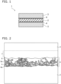
- FIG. 1 is a schematic view showing an example of a bonded body according to an embodiment.
- 1 is a bonded body
- 2 is a ceramic substrate
- 3 is a copper plate
- 4 is a bonding layer.
- FIG. 1 shows the bonded body 1 in which the copper plates 3 are respectively provided on both surface of the ceramic substrate 2 with the bonding layers 4 interposed therebetween.
- the longitudinal and lateral sizes of the ceramic substrate 2 and the copper plate 3 are the same as each other.
- the bonded body according to the embodiment is not limited to such a form, and may have a structure in which the copper plate 3 is provided only on one surface of the ceramic substrate 2.
- the longitudinal and lateral sizes of the ceramic substrate 2 and the copper plate 3 may be different from each other.
- a silicon nitride substrate, an aluminum nitride substrate, an aluminum oxide substrate, an Alumina zirconia substrate, etc. are examples of the ceramic substrate. It is favorable for the thickness of the ceramic substrate 2 to be not less than 0.1 mm and not more than 1 mm. When the substrate thickness is less than 0.1 mm, there is a possibility that the strength of the ceramic substrate 2 may decrease. Also, when the substrate thickness is greater than 1 mm, there is a possibility that the ceramic substrate may function as a thermal resistor, and the heat dissipation of the bonded body may be degraded.
- the three-point bending strength of the silicon nitride substrate is favorable for the three-point bending strength of the silicon nitride substrate to be not less than 600 MPa. Also, it is favorable for the thermal conductivity to be not less than 80 W/m K.
- the substrate thickness can be thinned by increasing the strength of the silicon nitride substrate. It is therefore favorable for the three-point bending strength of the silicon nitride substrate to be not less than 600 MPa, and more favorably not less than 700 MPa. Thereby, the substrate thickness of the silicon nitride substrate can be thinned to be not more than 0.40 mm, and even not more than 0.30 mm.
- the three-point bending strength of the aluminum nitride substrate is about 300 to 450 MPa.
- the thermal conductivity of the aluminum nitride substrate is not less than 160 W/m ⁇ K. Because the strength of the aluminum nitride substrate is low compared to the silicon nitride substrate, it is favorable for the substrate thickness to be not less than 0.60 mm.
- the three-point bending strength of the aluminum oxide substrate is about 300 to 450 MPa, the aluminum oxide substrate is inexpensive. Also, although the three-point bending strength of the Alumina zirconia substrate is high, i.e., about 550 MPa, the thermal conductivity of the Alumina zirconia substrate is about 30 to 50 W/m ⁇ K.
- the ceramic substrate 2 is one of a silicon nitride substrate or an aluminum nitride substrate.
- the silicon nitride substrate and the aluminum nitride substrate are nitride ceramic substrates.
- Nitride ceramics react with an active metal brazing material containing Ti to form titanium nitride.
- oxide ceramics react with an active metal brazing material containing Ti to form titanium oxide.
- An oxygen-free copper plate or a copper alloy plate can be used as the copper plate 3. It is favorable for the copper plate 3 to be oxygen-free copper. As described in JIS-H-3100, the oxygen-free copper has a copper purity of not less than 99.96 wt%.
- the bonding layer contains Cu, Ti, and a first element being one or two selected from Sn and In.
- Cu copper is an element that serves as a base material of the bonding layer. Even if Cu diffuses into the copper plate, it does not deteriorate the copper plate.
- Ti titanium is an effective element for forming a strong bond by reacting with the ceramic substrate.
- Sn (tin) or In (indium) is an element effective in lowering the melting point of the bonding brazing material that forms the bonding layer. As will be described later, it is effective to increase the heating rate in order to obtain the desired bonding layer. For that purpose, it is necessary to contain Sn or In.
- the bonding layer is characterized by including a Ti-rich region and a Ti-poor region.
- the ratio (M Ti /M E1 ) of the mass M Ti of Ti to the mass M E1 of the first element is not less than 0.5.
- the ratio (M Ti /M E1 ) of the mass M Ti of Ti to the mass M E1 of the first element is not more than 0.1.
- the Ti content in the Ti-rich region is higher than the Ti content in the Ti-poor region.
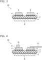
- FIG. 2 is a schematic view showing an example of the bonding layer according to the embodiment.
- 2 is the ceramic substrate
- 3 is the copper plate
- 4 is the bonding layer
- 4a is a Ti-aggregate layer
- 5 is the Ti-rich region
- 5a is a Ti intermediate amount region
- 6 is the Ti-poor region
- 7 is a diffusion region.
- the dotted regions are the Ti-rich region 5 and the Ti intermediate amount region 5a.
- the dot density of the Ti-rich region 5 is higher than that of the Ti intermediate amount region 5a.
- a cross section of the bonded body 1 is taken as a measurement area.
- the cross section of the bonded body 1 is parallel to a direction perpendicular to the surface of the ceramic substrate 2.
- only the bonding layer 4 is taken as the measurement area. In other words, the ceramic substrate 2 and the copper plate 3 are not included in the measurement area.
- the Ti-rich region 5 is a region in which the mass ratio (M Ti /M E1 ) is not less than 0.5.
- the Ti-poor region 6 is a region in which the mass ratio (M Ti /M E1 ) is not more than 0.1.
- the ceramic substrate 2 is bonded by a reaction between the ceramic substrate 2 and Ti in the brazing material. Therefore, a Ti aggregate layer is formed on the surface of the ceramic substrate 2.
- the ceramic substrate 2 is nitride ceramics
- the Ti-aggregate layer will be a titanium nitride (TiN) layer.
- the Ti aggregate layer will be a titanium oxide (TiO 2 ) layer.
- the mass ratio (M Ti /M E1 ) in the Ti-rich region is not particularly limited, it is preferably not more than 1.2.
- the mass ratio (M Ti /M E1 ) exceeds 1.2 it means that either the amount of Ti is large or the amount of Sn (or In) is small. In such a case, there is a possibility that the bondability will deteriorate when the heating rate is increased. Therefore, the mass ratio (M Ti /M E1 ) in the Ti-rich region is preferably not less than 0.5 and not more than 1.2.
- Ti-rich region 5 can suppress excessive diffusion of Sn (or In) into the copper plate. In other words, Ti has a trapping effect of retaining Sn in the bonding layer 4.
- the mass ratio (M Ti /M E1 ) in the Ti-poor region 6 is not more than 0.1.
- the lower limit of the mass ratio (M Ti /M E1 ) in the Ti-poor region 66 includes zero.
- the Ti amount of zero means that the amount is below the detection limit.
- a TiSn alloy exists in a portion of the Ti-rich region 5.
- the TiSn alloy may exist in a portion of the Ti-poor region 6.
- the main component of the Ti-aggregate layer 4 is titanium nitride or titanium oxide, as will be described later.
- the Ti-rich region and the Ti-poor region are distinguished from the Ti aggregate layer formed on the surface of the ceramic substrate 2.
- a region in which the mass ratio (M Ti /M E1 ) is not less than 0.2 and not more than 0.4 may exist in the measurement area.
- the region where the mass ratio (M Ti /M E1 ) is not less than 0.2 and not more than 0.4 is called the Ti intermediate amount region.
- the TiSn alloy in the Ti-rich region 5 and the Ti-poor region 6 may also contain intermetallic compounds.
- Sn 3 Ti 5 and Sn 5 Ti 6 are examples of the intermetallic compounds. Not less than 50% of the TiSn alloy is preferably Sn 3 Ti 5 or Sn 5 Ti 6 . The existence of Sn 3 Ti 5 or Sn 5 Ti 6 indicates that the bonding reaction successfully occurred.
- the ratio (M Cu /M E1 ) of the mass M Cu of Cu to the mass M E1 of the first element is preferably not less than 0.05 and not more than 0.4.
- the mass ratio (M Cu /M E1 ) is preferably not less than 3 and not more than 10.
- the Ti-rich region described above is mainly composed of a TiSn alloy that contains a large amount of Sn having a large atomic number.
- a cross section of the bonding layer is observed with a backscattered electron image of SEM, an element with a large atomic number appears whiter than an element with a small atomic number. Therefore, the TiSn alloy appears white when the backscattered electron image of SEM is observed with high contrast.
- the amount of TiSn alloy in the Ti-rich region is significantly higher than the amount of TiSn alloy in the Ti-poor region. In other words, in the bonding layer observed in the backscattered electron image, a region that appears white can be regarded as the Ti-rich region.
- the area observed white with high contrast exists in an area ratio of not less than 10% per the measurement area of 20 ⁇ m ⁇ 10 ⁇ m.
- the area ratio of the Ti-rich region can be obtained.
- the upper limit of the area ratio of the region that appears white is preferably 90%.
- Both the Ti-rich region 5 and the Ti-poor region 6 must exist within the measurement area of 20 ⁇ m ⁇ 10 ⁇ m.
- the area ratio of the Ti-rich region may be obtained in combination with the above-described SEM-EDX. As the atomic number of the element increases, the contrast in the backscattered electron image of the SEM appears whiter.
- the mass ratio (M Ti /M E1 ) in the Ti-rich region is not less than 0.5 and not more than 1.2, it becomes easy to distinguish between the Ti-rich region and the Ti-poor region by the contrast.
- the contrast of the backscattered electron image of the SEM can be changed depending on the apparatus. For this reason, it is effective to check by the shade of white. Therefore, the method using the backscattered electron image can be used as a simplified way of the method using the EDX.
- the area ratio of the Ti-rich region is preferably in the range not less than 10% and not more than 90%, more preferably not less than 20% and not more than 60%.
- the bonding layer comprises the Ti-poor region or the Ti intermediate amount region.
- the area ratio of the Ti-poor region is preferably in the range not less than 10% and not more than 50%.
- regions other than the Ti-rich region, the Ti intermediate amount region, and the Ti-poor region may exist. For example, when a Cu-Sn-Ti-C based brazing material is used, a Sn-free region may be formed.
- the Sn-free region does not correspond to any of the Ti-rich region, the Ti intermediate amount region, and the Ti-poor region. Therefore, when the Ti-rich region, the Ti intermediate amount region, and the Ti-poor region satisfy the above-described ranges, a region in which Sn or In does not exist may be provided.
- the mass ratio (M Ti /M E1 ) in the area on the ceramic substrate side is preferably greater than the mass ratio (M Ti /M E1 ) in the area on the copper plate side.
- the ratio (M Ti /M Sn ) of the mass M Ti of Ti to the mass M Sn of Sn is preferably less than 1 when the cross section of the bonding layer is analyzed.
- the ratio (M Ti /M In ) of the mass M Ti of Ti to the mass M In of In is preferably less than 1.
- Dividing the cross section of the bonding layer vertically into two halves means that a straight line perpendicular to the surface of the ceramic substrate is drawn from the bonding boundary between the ceramic substrate and the bonding layer to the bonding boundary between the bonding layer and the copper plate and another straight line parallel to the ceramic substrate surface is drawn from the center of the straight line.
- the bonding boundary between the ceramic substrate 2 and the bonding layer 4 is the bonding boundary between the ceramic substrate 2 and the Ti-aggregate layer 4a.
- the Ti-aggregate layer is a titanium nitride (TiN) layer.
- the bonding boundary between the bonding layer 4 and the copper plate 3 is the farthest point (the farthest point from the ceramic substrate 2) of the points where the components of the bonding layer are continuous and contact the copper plate 3 . Because the components of the bonding layer 4 contain Ti and the first element, the bonding boundary between the bonding layer 4 and the copper plate 3 is determined based on the diffusion state of these elements.
- the titanium nitride which is the Ti-aggregate layer, may contain titanium and nitrogen at an atomic ratio other than 1:1.
- the Ti-aggregate layer is titanium oxide.
- Various titanium oxides such as TiO 2 , TiO, and Ti 2 O 3 may exist as the Ti-aggregate layer.
- the bonding boundary is determined by replacing the aforementioned titanium nitride with titanium oxide.
- the mass ratio (M Ti /M E1 ) in the region on the ceramic substrate side being greater than the mass ratio (M Ti /M E1 ) in the region on the copper plate side means that the amount of Ti is small or the amount of the first element is large in the region of the bonding layer on the copper plate side.
- the mass ratio (M Ti /M Sn ) being less than 1 indicates that the amount of Sn is greater than the amount of Ti in the bonding layer.
- the mass ratio (M Ti /M In ) being less than 1 indicates that the amount of In is greater than the amount of Ti in the bonding layer.
- the height of the diffusion region is preferably not less than 100 ⁇ m.
- the diffusion amount of Sn or In from the boundary between the bonding layer and the copper plate to the copper plate is not less than 1 wt%
- the height of the diffusion region corresponds to the distance from the boundary between the bonding layer and the copper plate to the boundary between the region where the diffusion amount of Sn or In is not less than 1 wt% and the region where the diffusion amount of Sn or In is less than 1 wt% in the copper plate. More preferably, the height of the diffusion region is not more than 50 ⁇ m.
- a melting point of a CuSn alloy decreases as the amount of Sn increases.
- the CuSn alloy is formed in the copper plate.
- the amount of Sn diffusion is large, the amount of Sn in the CuSn alloy increases.
- the melting point of the copper plate is lowered, and the copper plate is likely to be distorted during the bonding process and the TCT test.
- the melting point of copper is 1085 °C.
- the amount of Sn in the CuSn alloy is not less than 50 wt%, the melting point of the CuSn alloy is 100 to 300 °C.
- the height of the diffusion region 7 where the amount of Sn or In diffused into the copper plate 3 is not less than 1 wt% is preferably not more than 100 ⁇ m, more preferably not more than 50 ⁇ m.
- the content of Sn or In in the copper plate can be regarded as the diffusion amount of Sn or In.
- the copper alloy plate containing Sn or In may be used as the copper plate. Sn or In is uniformly dispersed in the copper alloy plate.
- the content of Sn or In on the front surface side of the copper plate (so-called the surface of the copper plate) and the content on the back surface side of the copper plate (diffusion region 7) are measured, and the content on the front surface side is subtracted from the content on the back surface side to calculate the amount of diffusion.
- the back surface of the copper plate is the surface to be bonded with the ceramic substrate.
- the front surface is the surface opposite to the back surface and is not in contact with the bonding layer.
- the diffusion of Sn or In lowers the melting point of the copper alloy plate, so it is preferable to suppress the diffusion of Sn or In.
- the melting point of the copper alloy plate containing Sn or In is lower than the melting point of the oxygen-free copper plate containing no Sn or In. Therefore, the oxygen-free copper plate is preferably for the copper plate.
- the thickness of the copper plate is not less than 0.3 mm.
- the thickness of the copper plate 3 is preferably not less than 0.3 mm, more preferably not less than 0.6 mm. Because the bonded body according to the embodiment can narrow the diffusion region 7 in which Sn or In is diffused into the copper plate, it is possible to suppress distortion even if the copper plate is thick.
- the upper limit of the thickness of the copper plate 3 is not particularly limited, it is preferably not more than 3 mm, more preferably not more than 2 mm. Bonding is possible even if the thickness of the copper plate exceeds 3 mm. On the other hand, when the copper plate is too thick, the etching process is difficult. The etching process is performed to provide a pattern configuration to the copper plate. Therefore, the thickness of the copper plate is preferably not less than 0.3 mm and not more than 3 mm.
- the bonding layer 4 may contain elements other than Cu, Ti, Sn, and In. Examples of the elements other than these are not more than 20 wt% of Ag or not more than 2 wt% of carbon.
- the bonded body as described above is suitable for a circuit board.
- a semiconductor element can be mounted on the circuit board according to the embodiment, and the circuit board can be used for a semiconductor device.
- FIG. 3 is a schematic view showing an example of the circuit board according to the embodiment.
- FIG. 4 is a schematic view showing an example of the semiconductor device according to the embodiment.
- 8 is a copper circuit portion
- 9 is a heat dissipation plate
- 10 is a semiconductor element
- 11 is a lead frame
- 20 is a circuit board
- 30 is a semiconductor device.
- the copper plate 3 on the front side of the bonded body 1 is processed into the copper circuit portion 8, and the copper plate 3 on the back side is processed into the heat dissipation plate 9.
- the circuit board 20 is made by providing the circuit configuration to the copper plate 3 of the bonded body 1.
- the semiconductor element 10 is mounted on the copper circuit portion 8 of the circuit board 20.
- the lead frame 11 or the like may be mounted as necessary in the semiconductor device 30.
- the circuit board 20 has a structure in which two copper circuit portions 8 are provided, but the structure of the circuit board 20 is not limited to this example.
- the number or the sizes of the copper circuit portions 8 can be changed as required.
- the respective numbers of semiconductor elements 10 and lead frames 11 can also be changed arbitrarily.
- the copper plate 3 on the back side is used as the heat dissipation plate 9 in FIG. 3 , but the copper plates 3 on both sides may be provided with circuit configurations.
- the side surface of the copper circuit portion 8 and the side surface of the heat dissipation plate 9 may be inclined.
- the bonding layer 4. may be provided with a jutting portion that juts from the side edge of the copper circuit portion 8 or the side edge of the heat dissipation plate 9. It is preferable to use an etching process to provide the circuit configuration and to provide the inclined shape of the side surface of the copper plate.
- the manufacturing method is not limited, as long as the bonded body according to the embodiment has the above structure.
- an example of a method for obtaining the bonded body according to the embodiment with a high yield will be described.
- the ceramic substrate 2 is prepared.
- a silicon nitride substrate, an aluminum nitride substrate, an aluminum oxide substrate, an Alumina zirconia substrate, etc., are examples of the ceramic substrate 2.
- the Alumina zirconia substrate is a substrate in which aluminum oxide and zirconium oxide are mixed.
- the oxygen-free copper plate or the copper alloy plate can be used for the copper plate 3.
- the copper plate is preferably the oxygen-free copper.
- the oxygen-free copper is a copper plate having a copper purity of not less than 99.96 wt%, as specified in JIS-H-3100 (ISO1337, etc.).
- the bonding brazing material preferably contains not less than 50 mass% of Cu, not less than 4 mass% and not more than 30 mass% of Ti, not less than 5 mass% and not more than 40 mass% of one or two selected from Sn and In, not less than 0 mass% and not more than 20 mass% of Ag, not less than 0 mass% and not more than 2 mass% of Carbon.
- the bonding brazing material is prepared so that it can be bonded even if a rapid heating process with a heating rate of not less than 20 °C/min is performed.
- the bonding brazing material has an endothermic peak in the range of not less than 520 °C and not more than 590 °C in the DSC curve of the heating process at the heating rate of 20 °C/min.
- the DSC curve is obtained by applying heat to a sample and measuring the existence or absence of endothermic reaction and exothermic reaction using a Differential Scanning Calorimeter (DSC).
- DSC Differential Scanning Calorimeter
- a peak in the negative direction is the endothermic reaction
- a peak in the positive direction is the exothermic reaction.
- the endothermic reaction indicates that the sample is melting, decomposing, etc.
- the exothermic reaction indicates that the constituent elements of the sample react with each other to form or solidify a compound (including alloying). Larger peak indicates larger heat of the reaction.
- the peak in the negative direction is called an endothermic peak
- the peak in the positive direction is called an exothermic peak.
- the apex of the peak is called a peak top.
- the difference between the local maximum point and the local minimum point of the peak is called a peak height.
- the endothermic peak is in the negative direction, so it goes up, then down, then up.
- the endothermic peak includes a change of a local maximum point ⁇ a local minimum point ⁇ a local maximum point.
- the local minimum point (the lowest point) is the peak top.
- the larger value (larger peak in the positive direction) is taken as the top maximal point.
- the peak height is the value obtained by subtracting the local minimum point from the top maximal point.
- the exothermic peak is in the positive direction, so it goes down, then up, then down.
- the exothermic peak includes a change of a local minimum point ⁇ a local maximum point ⁇ a local minimum point.
- the local maximum point (the highest point) is the peak top.
- the smaller value (larger peak in the negative direction) is taken as a bottom minimal point.
- the peak height is the value obtained by subtracting the bottom minimal point from the local maximum point.
- the end point of the endothermic peak may appear as the exothermic peak (peak in the positive direction), but it is counted as the exothermic peak here.
- Each peak may be obtained by drawing a baseline.
- TGA-DSC simultaneous thermal analysis device STA449-F3-Jupiter manufactured by NETZSCH or a device having equivalent performance is used.
- the measurement is carried out in an Ar (argon) flow by dropping an appropriate amount of brazing material into an alumina container. The measurement is carried out with the lid of the alumina container closed. It is necessary to prevent the brazing material from reacting with the atmosphere by measuring in the Ar atmosphere.
- the amount (mg) dropped is measured with a balance. Not less than 15 mg of the solid content of the sample is prepared.
- a temperature profile for obtaining the DSC curve consists of the heating process described above, a holding process, and a cooling process.
- the heating process is a process of raising the temperature from room temperature to 950 °C at the heating rate of 20 °C/min.
- the holding process is a process of holding at 950 °C for 20 minutes.
- the cooling process is a process of lowering the temperature from 950 °C to room temperature at a cooling rate of 20 °C/min.
- the holding process is performed after the heating process, and the cooling process is performed after the holding process.
- the DSC curve of the heating process with the heating rate of 20 °C/min may be referred to as the DSC curve of the heating process.
- the DSC curve of the cooling process with the cooling rate of 20 °C/min may be referred to as the DSC curve of the cooling process.
- a difference in heat flow of not less than 0.02 mW/mg between the baseline and the apex of a protrusion was counted as a peak .
- FIG. 5 shows the DSC curve (500 to 600 °C) of the heating process of the bonding brazing material used in an example 1
- FIG. 6 shows the DSC curve (700 to 900 °C) of the heating process of the bonding brazing material used in the example 1.
- the horizontal axis represents temperature (°C)
- the vertical axis represents heat flow (mW/mg).
- the heat flow is denoted as DSC.
- the DSC curve of the heating process at the heating rate of 20 °C/min has an endothermic peak in the range of not less than 520 °C and not more than 590 °C. Moreover, it is preferable to have an endothermic peak within the range of not less than 730 °C to 800 °C of the heating process.
- the endothermic peak within the range of not less than 520 °C and not more than 590 °C in the DSC curve of the heating process is called a first endothermic peak.
- the largest peak is taken as the first endothermic peak.
- the largest peak indicates a large peak on the minus side.
- the endothermic peak within the range of not less than 730 °C to 900 °C in the DSC curve of the heating process is called a second endothermic peak.
- the largest peak is taken as the second endothermic peak.
- the largest peak indicates a large peak on the minus side.
- FIG. 5 is a chart showing an example of the first endothermic peak.
- FIG. 6 is a chart showing an example of the second endothermic peak.
- the brazing material containing no Ag preferably has the second endothermic peak within the range of not less than 730 °C and not more than 800 °C as shown in FIG. 6 .
- the first endothermic peak indicates the decomposition reaction of TiH 2 .
- the decomposed hydrogen has the effect of removing impurity oxygen in the brazing material and activating metal components.
- AgCuSnTi brazing material containing not less than 40 mass% of Ag is used as a conventional active metal brazing material.
- the decomposition reaction of TiH 2 occurs at 480-500 °C. In other words, there is no first endothermic peak in the DSC curve of the conventional active metal brazing material. By shifting the decomposition reaction of TiH 2 to the high-temperature side, the nitriding of the bonding brazing material can be suppressed.
- the Ti-aggregate layer is formed on the surface of the ceramic substrate.
- the second endothermic peak indicates the melting reaction between Cu and the first element.
- Cu and the first element are elements that form the base material of the bonding brazing material. Therefore, the second endothermic peak indicates that the reaction occurs in which the bonding brazing material melts and a liquid phase is generated.
- the decomposition reaction of TiH 2 occurs at 480-500 °C. That is, there is no first endothermic peak in the conventional active metal brazing material.
- the temperature difference between the peak indicating the decomposition reaction of TiH 2 and the second endothermic peak indicating the melting reaction between Cu and the first element can be reduced by using the bonding brazing material that occurs the first endothermic peak. As a result, the bondability can be maintained even if the heating rate in the bonding process is increased.
- the DSC curve of the cooling process at the cooling rate of 20 °C/min has an exothermic peak.
- the exothermic peak in the cooling process indicates that the formation or solidification of a compound (an alloy) in the bonding layer occurs.
- the thermal stress is greatest when the molten brazing material solidifies. This is because members having different coefficients of thermal expansion are constrained after the bonding boundary is formed, and the stress is generated during cooling due to the difference in the thermal expansion. Therefore, it is preferable that the DSC curve in the cooling process has the exothermic peak at not more than 850 °C.
- the DSC curve may have two or more exothermic peaks. Having two or more exothermic peaks indicates that the formation or the solidification of the compound (alloy) in the bonding layer is performed in multiple steps. This improves the stress relaxation effect of the bonded body.
- the DSC curve of the cooling process at the cooling rate of 20 °C/min has an exothermic peak at not less than 450 °C and not more than 550 °C.
- the exothermic peak at not less than 450 °C and not more than 550 °C in the DSC curve of the cooling process at the cooling rate of 20 °C/min is called a first exothermic peak.
- the largest peak is taken as the first exothermic peak.
- the exothermic peak in the cooling process is less than 450 °C, the solidification temperature is too low, and there is a possibility that the reliability of the bonding will decrease.
- the exothermic peak is high, i.e., greater than 550 °C, the thermal stress may increase.
- the peak top temperature of the first exothermic peak is preferably lower.
- the first endothermic peak is mainly caused by the decomposition reaction of TiH 2 .
- the first exothermic peak in the cooling process is an exothermic reaction caused by solidification of the bonding layer or formation of Ti compounds.
- Such bonding brazing material can be bonded at the heating rate of not less than 20 °C/min or at the cooling process of not less than 20 °C/min.
- the bonding atmosphere may be in a vacuum or in a nitrogen atmosphere.
- the vacuum means an atmosphere of not more than 1 ⁇ 10 -3 Pa.
- the nitrogen atmosphere means an atmosphere containing not less than 70 vol% of nitrogen.
- Argon gas or air atmosphere is an example of a component other than nitrogen.
- the bonding brazing material preferably contains not less than 50 mass% of Cu, not less than 4 mass% and not more than 30 mass% of Ti, not less than 5 mass% and not more than 40 mass% of one or two selected from Sn and In, not less than 0 mass% and not more than 20 mass% of Ag, not less than 0 mass% and not more than 2 mass% of Carbon.
- the total content of Cu, Ti, and the first element is preferably not less than 80 mass%, more preferably not less than 90 mass% and not more than 100 mass%. Also, the total content of Cu and the first element is preferably not less than 70 mass%.
- the melting point of the brazing material can be raised by substantially lowering the content proportion of Ag. This makes it possible to obtain the brazing material having the desired DSC curve even if the heating rate and cooling rate are increased.
- the average grain size D 50 is preferably not more than 12.0 ⁇ m, more preferably not more than 10.0 ⁇ m.
- the average grain size D 50 of TiH 2 powder is preferably not more than 6.0 ⁇ m, more preferably not more than 4.0 ⁇ m.
- the average grain size D 50 of Sn powder or In powder is preferably not more than 16.0 ⁇ m, more preferably not more than 14.0 ⁇ m.
- the average grain size D 50 of C powder is preferably not more than 6.0 ⁇ m, more preferably not more than 4.0 ⁇ m.
- the average grain size D 50 of Ag powder is preferably not more than 3.0 ⁇ m, more preferably not more than 2.0 ⁇ m.
- the average grain size D 50 of the Cu powder is preferably smaller than the average grain size D 50 of the Sn powder or In powder.
- Cu and the first element are the base materials for the brazing material composition.
- Sn and In are elements having lower melting points compared with Cu.
- the difference between the heating rate and the cooling rate is not more than 20 °C/min. That is, it is preferable to satisfy
- ⁇ 20 °C/min By heating the brazing material layer, the melting reaction and the solidification reaction occur. These reactions occur in the heating process and the cooling process.
- the stress caused by the reactions can be homogenized. Thereby, problems such as the warp can be suppressed. It is also effective in controlling the area ratios of the Ti-rich region, the Ti-poor region, and the Ti intermediate amount region.
- a process of bonding the ceramic substrate and the copper plate is performed using the brazing material as described above.
- a brazing material paste is prepared by mixing a bonding brazing material with an organic substance.
- the brazing material paste is applied to the surface of the ceramic substrate 2 (or the copper plate 3) to form a brazing material paste layer.
- the copper plate 3 (or the ceramic substrate 2) is placed on the brazing material paste layer.
- the thermal bonding process is performed in vacuum or in the nitrogen atmosphere.
- vacuum means under pressure of not more than 1 ⁇ 10 -3 Pa.
- the nitrogen atmosphere is an atmosphere containing not less than 70 vol% of nitrogen.
- the nitrogen atmosphere preferably has a nitrogen content of not less than 70 vol%, more preferably not less than 85 vol% and not more than 100 vol%.
- the nitrogen atmosphere may contain argon gas or the atmosphere in addition to nitrogen.
- the heating rate is set to not less than 20 °C/min.
- the heating rate was not more than 5 °C/min.
- the upper limit of the heating rate is not particularly limited, it is preferably not more than 100 °C/min.
- the heating rate is preferably not less than 20 °C/min and not more than 100 °C/min, more preferably not less than 30 °C/min and not more than 70 °C/min.
- the temperature is raised to the bonding temperature by the heating process.
- the bonding temperature is set to not less than 750 °C.
- the bonding temperature is set to a temperature higher than the peak top temperature of the second endothermic peak.
- the second endothermic peak is at 730-800 °C.
- the bonding temperature is preferably not less than 750 °C, more preferably not less than 800 °C.
- the upper limit of the bonding temperature is preferably not more than 1000 °C. When the temperature is high, i.e., greater than 1000 °C, the temperature is close to the melting point of copper (1085 °C), and the copper plate may be deformed.
- the bonding temperature is preferably held for not less than 10 minutes.
- the time during which the bonding temperature is held is referred to as a heat-holding time.
- the heat-holding time is preferably not less than 10 minutes and not more than 100 minutes. When the heat-holding time is less than 10 minutes, there is a possibility that the brazing material will not have enough time to melt or solidify. Also, when it is longer than 100 minutes, Sn or In may diffuse too much into the copper plate.
- the cooling process is a process of cooling from the bonding temperature to room temperature.
- the cooling rate is set to not less than 20 °C/min. In the conventional active metal bonding method, the cooling rate was about 5 °C/min.
- the upper limit of the cooling rate is not particularly limited, it is preferably not more than 100 °C/min. When it is high, i.e., greater than 100 °C/min, the bondability may deteriorate. Therefore, the cooling rate is preferably not less than 20 °C/min and not more than 100 °C/min, more preferably not less than 30 °C/min and not more than 70 °C/min.
- the thermal bonding process may be performed while placing a weight on the bonded body 1.
- the bonded body 1 can be made. By increasing the heating rate in the heating process and the cooling rate in the cooling process, the amount of heat applied to the bonded body 1 can be reduced. As a result, the distribution of Ti and the first element in the bonding layer can be controlled. Also, the amount of Sn (or In) diffused into the copper plate can be reduced.
- the amount of heat applied to the bonded body 1 can be reduced, warp of the bonded body 1 or distortion of the copper plate 3 can be reduced.
- the obtained bonded body 1 is etched and processed into the circuit board 20. Multiple components can be obtained as needed. Obtaining multiple components is a method of obtaining small bonded bodies by cutting a large bonded body. There is also a method of subdividing the bonded body or a method of subdividing the ceramic circuit board. Scribing may be performed to easily subdivide. Scribing may be performed to easily subdivide. The explanations of past applications are used.
- Bonding brazing materials shown in Table 1 and Table 2 were prepared.
- Table 1 shows the grain sizes of the raw material powders and Table 2 shows the composition ratio.
- Composition ratio (mass%) Cu powder Sn powder TiH 2 powder C powder Ag powder Example 1 59.3 30 10 0.7 - Example 2 71.8 21 7 0.2 - Example 3 73 15 12 - - Example 4 60 32 8 - - Example 5 62.9 28 9 0.1 - Comparative example 1 42 5 3 - 50
- Brazing material pastes were made by mixing the bonding brazing material components according to the examples and the comparative example with an organic binder. The DSC curve was measured for each brazing material pastes using the DSC.
- TGA-DSC simultaneous thermal analysis apparatus STA449-F3-Jupiter manufactured by NETZSCH was used as the DSC.
- the measurement was carried out in an Ar flow by dropping an appropriate amount of the brazing material into an alumina container. The measurement was performed with the lid of the alumina container closed.
- the temperature program consisted of the heating rate of 20 °C/min, 950 °Cx20 min holding, and the cooling rate of 20 °C/min. 15 mg of the solid content of the sample was used.
- the bonding brazing materials according to the examples had the first endothermic peak and the second endothermic peak.
- the endothermic peak indicating the decomposition reaction of TiH 2 was below 520 °C. That is, no first endothermic peak was observed.
- a silicon nitride substrate was prepared as the ceramic substrate.
- the silicon nitride substrate having a thermal conductivity of 90 W/m ⁇ K, a three-point bending strength of 600 MPa, and 50 mm long ⁇ 40 mm wide ⁇ 0.32 mm thick was used.
- As the copper plate the oxygen-free copper plate having 50 mm long ⁇ 40 mm wide ⁇ 0.5 mm thick was prepared.
- the brazing material paste of 30 ⁇ m was applied to both surfaces of the ceramic substrate, and the copper plates was respectively placed thereon.
- a bonded body was manufactured by the above processes. Ten bonded bodies according to each of the examples and the comparative example were manufactured.
- the cross-sectional structure of the obtained bonded body was observed.
- the cross section of the bonded body was observed by SEM-EDX.
- the measurement area of 20 ⁇ m ⁇ 10 ⁇ m in the bonding layer was observed to observe the Ti-rich region and the Ti-poor region.
- arbitrary three areas that do not overlap each other were observed.
- the result in which they were observed at all three areas was described as "yes", and the result in which they were not observed at even one area was described as "no".
- the area ratio the lower limit and upper limit of the measurement results were recorded.
- the mass ratio of Cu and Sn the average value of the ratio of the mass of Cu to the mass of Sn was calculated.
- a diffusion region of Sn into the copper plate was also observed.
- a region where the ratio (M Ti /M Sn ) of the mass M Ti of Ti to the mass M Sn of Sn was not less than 0.5 was taken as the Ti-rich region.
- a region where the mass ratio (M Ti /M Sn ) was not more than 0.1 was taken as the Ti-poor region.
- the Ti-rich region and the Ti-poor region were observed in the bonding layer.
- the mass ratio (M Ti /M Sn ) in the Ti-rich region was within the range of not less than 0.5 and not more than 1.2.
- one or two intermetallic compounds of Sn 3 Ti 5 and Sn 5 Ti 6 were detected in the Ti-rich region and the Ti-poor region.
- the region that appeared white in the backscattered electron image at high contrast almost matched the Ti-rich region identified from the SEM-EDX analysis results.
- the area ratio of the Ti-rich region it is found that the investigating method using the SEM backscattered electron image is effective.
- the height of the Sn diffusion region into the copper plate was also small, i.e., not more than 100 ⁇ m, further not more than 50 ⁇ m. It is found that the brazing material having the DSC curve with the predetermined peak at the heating rate and the cooling rate of 20 °C/min has the effect of suppressing the diffusion of Sn into the copper plate.
- the warp amount of the obtained bonded body and the bonding strength of the copper plate were measured.
- the warp amount was measured on the long side.
- the pieces were evaluated as best products ( ⁇ ).
- the pieces were evaluated as good products ( ⁇ ).
- the pieces were evaluated as good products ( ⁇ ).
- the pieces were evaluated as defective products ( ⁇ ).
- the peel strength was used as the bonding strength of the copper plate.
- a sample for peel test was prepared in each of the examples and the comparative example. The samples were prepared by bonding a strip-shaped copper plate to the ceramic substrate. At that time, one end of the copper plate was bonded so as to protrude from the ceramic substrate. Peel strength was measured by pulling the protruding copper plate vertically. The results are shown in Table 7.
- Example 1 An example in which the heating rate and the cooling rate of the example 1 are set to 5 °C/min was referred to as the reference example 1.
- [Table 7] Amount of warp Bonding strength (kN/mm) Example 1 ⁇ 15 Example 2 ⁇ 17 Example 3 ⁇ 19 Example 4 ⁇ 15 Example 5 ⁇ 15 Comparative example 1 ⁇ 13 Reference example 1 ⁇ 6 Reference example 2 ⁇ 3
- the bonded bodies according to the examples were excellent in the warp amount and the bonding strength.
- the comparative example 1 because the amount of Ag was large, bonding was not successfully performed when the heating rate and cooling rate were high. Also, regarding an example in which the difference between the heating rate and the cooling rate exceeded 20 °C/min like the example 5, deterioration in the warp amount was observed. Therefore, it is found that the difference between the heating rate and the cooling rate is preferably not more than 20 °C/min.
- the bonding brazing materials of the examples are suitable for the fast-bonding process with the heating rate of not less than 20 °C/min. The same applies to the reference example 2 as well.
- the bonding brazing material containing a large amount of Ag progressed in nitridation, resulting in a decrease in the bonding strength.
- the brazing material has the DSC curve with the predetermined peak at the heating rate and the cooling rate of 20 °C/min, excellent bondability can be obtained even if the heating rate and cooling rate in the bonding process are increased, i.e., not less than 20 °C/min. Therefore, it is found that the bonded body according to the embodiment has a small warp amount and is excellent in mass productivity.
Landscapes
- Engineering & Computer Science (AREA)
- Chemical & Material Sciences (AREA)
- Ceramic Engineering (AREA)
- Microelectronics & Electronic Packaging (AREA)
- Materials Engineering (AREA)
- Structural Engineering (AREA)
- Organic Chemistry (AREA)
- Inorganic Chemistry (AREA)
- Manufacturing & Machinery (AREA)
- Mechanical Engineering (AREA)
- Ceramic Products (AREA)
- Parts Printed On Printed Circuit Boards (AREA)
Applications Claiming Priority (2)
| Application Number | Priority Date | Filing Date | Title |
|---|---|---|---|
| JP2020126589 | 2020-07-27 | ||
| PCT/JP2021/026928 WO2022024832A1 (ja) | 2020-07-27 | 2021-07-19 | 接合体、回路基板、半導体装置、及び接合体の製造方法 |
Publications (2)
| Publication Number | Publication Date |
|---|---|
| EP4190764A1 true EP4190764A1 (de) | 2023-06-07 |
| EP4190764A4 EP4190764A4 (de) | 2024-08-21 |
Family
ID=80036838
Family Applications (1)
| Application Number | Title | Priority Date | Filing Date |
|---|---|---|---|
| EP21850137.7A Pending EP4190764A4 (de) | 2020-07-27 | 2021-07-19 | Verbindungskörper, schaltungssubstrat, halbleiterbauelement und verfahren zur herstellung eines verbindungskörpers |
Country Status (5)
| Country | Link |
|---|---|
| US (1) | US12431406B2 (de) |
| EP (1) | EP4190764A4 (de) |
| JP (1) | JP7644763B2 (de) |
| CN (2) | CN119285367A (de) |
| WO (1) | WO2022024832A1 (de) |
Cited By (1)
| Publication number | Priority date | Publication date | Assignee | Title |
|---|---|---|---|---|
| EP4227284A4 (de) * | 2020-10-07 | 2025-09-03 | Toshiba Kk | Verbundener körper, keramiksubstrat für eine schaltung und halbleiterbauelement |
Families Citing this family (3)
| Publication number | Priority date | Publication date | Assignee | Title |
|---|---|---|---|---|
| US20230395445A1 (en) * | 2022-06-06 | 2023-12-07 | Intel Corporation | Glass core architectures with dielectric buffer layer between glass core and metal vias and pads |
| CN119403774A (zh) * | 2022-07-05 | 2025-02-07 | 株式会社东芝 | 接合体、陶瓷电路基板、半导体装置、以及接合体的制造方法 |
| JP7721035B2 (ja) * | 2023-02-17 | 2025-08-15 | 株式会社東芝 | 接合体およびそれを用いたセラミックス回路基板 |
Family Cites Families (14)
| Publication number | Priority date | Publication date | Assignee | Title |
|---|---|---|---|---|
| JPH0597532A (ja) * | 1991-10-08 | 1993-04-20 | Toshiba Corp | 接合用組成物 |
| WO2012015546A1 (en) | 2010-07-30 | 2012-02-02 | Exxonmobil Upstream Research Company | Systems and methods for using multiple cryogenic hydraulic turbines |
| JP6319643B2 (ja) * | 2012-02-29 | 2018-05-09 | 日立金属株式会社 | セラミックス−銅接合体およびその製造方法 |
| JP6266918B2 (ja) * | 2013-08-07 | 2018-01-24 | 京セラ株式会社 | セラミック体とNi−Cr−Fe合金との接合体、およびセラミック体とNi−Cr−Fe合金との接合方法 |
| JP6430382B2 (ja) * | 2013-08-08 | 2018-11-28 | 株式会社東芝 | 回路基板および半導体装置 |
| JP6256176B2 (ja) | 2014-04-25 | 2018-01-10 | 三菱マテリアル株式会社 | 接合体の製造方法、パワーモジュール用基板の製造方法 |
| JP6621402B2 (ja) * | 2014-04-30 | 2019-12-18 | 日本碍子株式会社 | セラミックス部材と金属部材との接合体及びその製法 |
| EP3358614B1 (de) * | 2015-09-28 | 2022-12-14 | Kabushiki Kaisha Toshiba | Schaltsubstrat und halbleiterbauelement |
| EP3460838B1 (de) * | 2016-05-19 | 2021-02-24 | Mitsubishi Materials Corporation | Substrat für leistungsmodule |
| EP3492441B1 (de) | 2016-07-28 | 2024-10-16 | Kabushiki Kaisha Toshiba | Verbundener körper, leiterplatte und halbleiterbauelement |
| JP6965768B2 (ja) * | 2017-02-28 | 2021-11-10 | 三菱マテリアル株式会社 | 銅/セラミックス接合体、絶縁回路基板、及び、銅/セラミックス接合体の製造方法、絶縁回路基板の製造方法 |
| KR102516917B1 (ko) | 2017-04-25 | 2023-03-31 | 덴카 주식회사 | 세라믹스 회로 기판 및 그 제조 방법과 그것을 사용한 모듈 |
| WO2019146464A1 (ja) * | 2018-01-25 | 2019-08-01 | 三菱マテリアル株式会社 | 銅/セラミックス接合体、絶縁回路基板、及び、銅/セラミックス接合体の製造方法、絶縁回路基板の製造方法 |
| WO2021235387A1 (ja) * | 2020-05-20 | 2021-11-25 | 株式会社 東芝 | 接合体、セラミックス銅回路基板、及び半導体装置 |
-
2021
- 2021-07-19 EP EP21850137.7A patent/EP4190764A4/de active Pending
- 2021-07-19 WO PCT/JP2021/026928 patent/WO2022024832A1/ja not_active Ceased
- 2021-07-19 CN CN202411392578.6A patent/CN119285367A/zh active Pending
- 2021-07-19 JP JP2022540197A patent/JP7644763B2/ja active Active
- 2021-07-19 CN CN202180059558.5A patent/CN116134004B/zh active Active
-
2022
- 2022-12-27 US US18/146,626 patent/US12431406B2/en active Active
Cited By (1)
| Publication number | Priority date | Publication date | Assignee | Title |
|---|---|---|---|---|
| EP4227284A4 (de) * | 2020-10-07 | 2025-09-03 | Toshiba Kk | Verbundener körper, keramiksubstrat für eine schaltung und halbleiterbauelement |
Also Published As
| Publication number | Publication date |
|---|---|
| WO2022024832A1 (ja) | 2022-02-03 |
| EP4190764A4 (de) | 2024-08-21 |
| JP7644763B2 (ja) | 2025-03-12 |
| US12431406B2 (en) | 2025-09-30 |
| JPWO2022024832A1 (de) | 2022-02-03 |
| CN119285367A (zh) | 2025-01-10 |
| CN116134004A (zh) | 2023-05-16 |
| CN116134004B (zh) | 2024-10-25 |
| US20230135530A1 (en) | 2023-05-04 |
Similar Documents
| Publication | Publication Date | Title |
|---|---|---|
| US12431406B2 (en) | Bonded body, circuit board, semiconductor device, and method for manufacturing bonded body | |
| US12347744B2 (en) | Bonded body including titanium alloy at bonding boundary | |
| US12115603B2 (en) | Bonded body, ceramic copper circuit substrate, and semiconductor device | |
| US20230187310A1 (en) | Bonded body, ceramic circuit substrate, and semiconductor device | |
| US12240218B2 (en) | Bonded assembly, and ceramic circuit substrate and semiconductor device using the same | |
| US20240079238A1 (en) | Bonded object production method and production method for ceramic circuit substrate using same | |
| US20250098065A1 (en) | Bonded body and ceramic circuit board using same | |
| US20250048563A1 (en) | Bonded body, ceramic copper circuit board, method for manufacturing bonded body, and method for manufacturing ceramic copper circuit board | |
| EP4108377A1 (de) | Hartlötfüllmaterial, verbundener körper, keramische leiterplatte und verfahren zur herstellung eines verbundenen körpers | |
| EP4585581A1 (de) | Kupfer/keramik verbundkörper und isolierte leiterplatte | |
| US20230260868A1 (en) | Bonded body, ceramic-copper circuit board, and semiconductor device |
Legal Events
| Date | Code | Title | Description |
|---|---|---|---|
| STAA | Information on the status of an ep patent application or granted ep patent |
Free format text: STATUS: THE INTERNATIONAL PUBLICATION HAS BEEN MADE |
|
| PUAI | Public reference made under article 153(3) epc to a published international application that has entered the european phase |
Free format text: ORIGINAL CODE: 0009012 |
|
| STAA | Information on the status of an ep patent application or granted ep patent |
Free format text: STATUS: REQUEST FOR EXAMINATION WAS MADE |
|
| 17P | Request for examination filed |
Effective date: 20221223 |
|
| AK | Designated contracting states |
Kind code of ref document: A1 Designated state(s): AL AT BE BG CH CY CZ DE DK EE ES FI FR GB GR HR HU IE IS IT LI LT LU LV MC MK MT NL NO PL PT RO RS SE SI SK SM TR |
|
| DAV | Request for validation of the european patent (deleted) | ||
| DAX | Request for extension of the european patent (deleted) | ||
| RAP3 | Party data changed (applicant data changed or rights of an application transferred) |
Owner name: TOSHIBA MATERIALS CO., LTD. Owner name: KABUSHIKI KAISHA TOSHIBA |
|
| REG | Reference to a national code |
Ref country code: DE Ref legal event code: R079 Free format text: PREVIOUS MAIN CLASS: C04B0037020000 Ipc: B23K0035300000 |
|
| A4 | Supplementary search report drawn up and despatched |
Effective date: 20240718 |
|
| RIC1 | Information provided on ipc code assigned before grant |
Ipc: H01L 23/373 20060101ALN20240712BHEP Ipc: H05K 3/38 20060101ALI20240712BHEP Ipc: H05K 1/03 20060101ALI20240712BHEP Ipc: C04B 37/02 20060101ALI20240712BHEP Ipc: B23K 35/30 20060101AFI20240712BHEP |
|
| RAP1 | Party data changed (applicant data changed or rights of an application transferred) |
Owner name: NITERRA MATERIALS CO., LTD. |