EP4200623B1 - Dispositif et procédé pour détecter une tension alternative - Google Patents
Dispositif et procédé pour détecter une tension alternative Download PDFInfo
- Publication number
- EP4200623B1 EP4200623B1 EP21765622.2A EP21765622A EP4200623B1 EP 4200623 B1 EP4200623 B1 EP 4200623B1 EP 21765622 A EP21765622 A EP 21765622A EP 4200623 B1 EP4200623 B1 EP 4200623B1
- Authority
- EP
- European Patent Office
- Prior art keywords
- voltage
- alternating voltage
- coupler
- input
- zero
- Prior art date
- Legal status (The legal status is an assumption and is not a legal conclusion. Google has not performed a legal analysis and makes no representation as to the accuracy of the status listed.)
- Active
Links
Images
Classifications
-
- G—PHYSICS
- G01—MEASURING; TESTING
- G01R—MEASURING ELECTRIC VARIABLES; MEASURING MAGNETIC VARIABLES
- G01R19/00—Arrangements for measuring currents or voltages or for indicating presence or sign thereof
- G01R19/175—Indicating the instants of passage of current or voltage through a given value, e.g. passage through zero
-
- H—ELECTRICITY
- H02—GENERATION; CONVERSION OR DISTRIBUTION OF ELECTRIC POWER
- H02M—APPARATUS FOR CONVERSION BETWEEN AC AND AC, BETWEEN AC AND DC, OR BETWEEN DC AND DC, AND FOR USE WITH MAINS OR SIMILAR POWER SUPPLY SYSTEMS; CONVERSION OF DC OR AC INPUT POWER INTO SURGE OUTPUT POWER; CONTROL OR REGULATION THEREOF
- H02M1/00—Details of apparatus for conversion
- H02M1/0003—Details of control, feedback or regulation circuits
- H02M1/0016—Control circuits providing compensation of output voltage deviations using feedforward of disturbance parameters
-
- H—ELECTRICITY
- H02—GENERATION; CONVERSION OR DISTRIBUTION OF ELECTRIC POWER
- H02M—APPARATUS FOR CONVERSION BETWEEN AC AND AC, BETWEEN AC AND DC, OR BETWEEN DC AND DC, AND FOR USE WITH MAINS OR SIMILAR POWER SUPPLY SYSTEMS; CONVERSION OF DC OR AC INPUT POWER INTO SURGE OUTPUT POWER; CONTROL OR REGULATION THEREOF
- H02M1/00—Details of apparatus for conversion
- H02M1/08—Circuits specially adapted for the generation of control voltages for semiconductor devices incorporated in static converters
- H02M1/083—Circuits specially adapted for the generation of control voltages for semiconductor devices incorporated in static converters for the ignition at the zero crossing of the voltage or the current
-
- H—ELECTRICITY
- H02—GENERATION; CONVERSION OR DISTRIBUTION OF ELECTRIC POWER
- H02M—APPARATUS FOR CONVERSION BETWEEN AC AND AC, BETWEEN AC AND DC, OR BETWEEN DC AND DC, AND FOR USE WITH MAINS OR SIMILAR POWER SUPPLY SYSTEMS; CONVERSION OF DC OR AC INPUT POWER INTO SURGE OUTPUT POWER; CONTROL OR REGULATION THEREOF
- H02M3/00—Conversion of DC power input into DC power output
- H02M3/02—Conversion of DC power input into DC power output without intermediate conversion into AC
- H02M3/04—Conversion of DC power input into DC power output without intermediate conversion into AC by static converters
- H02M3/10—Conversion of DC power input into DC power output without intermediate conversion into AC by static converters using discharge tubes with control electrode or semiconductor devices with control electrode
- H02M3/145—Conversion of DC power input into DC power output without intermediate conversion into AC by static converters using discharge tubes with control electrode or semiconductor devices with control electrode using devices of a triode or transistor type requiring continuous application of a control signal
- H02M3/155—Conversion of DC power input into DC power output without intermediate conversion into AC by static converters using discharge tubes with control electrode or semiconductor devices with control electrode using devices of a triode or transistor type requiring continuous application of a control signal using semiconductor devices only
- H02M3/156—Conversion of DC power input into DC power output without intermediate conversion into AC by static converters using discharge tubes with control electrode or semiconductor devices with control electrode using devices of a triode or transistor type requiring continuous application of a control signal using semiconductor devices only with automatic control of output voltage or current, e.g. switching regulators
- H02M3/158—Conversion of DC power input into DC power output without intermediate conversion into AC by static converters using discharge tubes with control electrode or semiconductor devices with control electrode using devices of a triode or transistor type requiring continuous application of a control signal using semiconductor devices only with automatic control of output voltage or current, e.g. switching regulators including plural semiconductor devices as final control devices for a single load
Definitions
- the invention relates to a device for detecting alternating voltage, comprising input terminals for applying an alternating voltage to be detected and output terminals at which the presence of the alternating voltage is indicated.
- the input terminals and the output terminals are galvanically isolated from one another by a coupler, wherein a control element of the coupler is supplied with operating current by the applied alternating voltage, and a switching element of the coupler is connected to the output terminals.
- the invention further relates to a method for detecting alternating voltage, which can be carried out in particular with the aforementioned device.
- Such devices are used to check for the presence of alternating voltage at specific nodes in an electrical installation, for example, by reading the output connections from a higher-level monitoring device.
- a common application is to determine the correct functioning of relays or contactors, circuit breakers, residual current devices, or load break switches by detecting the presence of alternating voltage (output side) at switching contacts and comparing it with the specified switching state of the device being tested.
- the AC voltage to be detected is usually a low voltage with a voltage of more than 60 V, such as a lighting mains voltage.
- the higher-level monitoring device can be, for example, an industrial automation system used for monitoring or control purposes.
- the monitoring device can also be a gateway or a data logger, which then only performs monitoring.
- the inputs of such monitoring devices are usually designed to detect a switching signal or a protective extra-low voltage, for example 12 volts (V) or 24 V.
- the aforementioned device for detecting alternating voltage transmits the information about the presence of alternating voltage in the form of a galvanically isolated switching signal to the monitoring device.
- the coupler is usually an optocoupler with a light-emitting diode (LED) as the control element for galvanic isolation.
- the optocoupler is supplied with operating current from the applied alternating voltage so that the switching element of the optocoupler, usually a phototransistor, becomes conductive.
- a series circuit comprising a rectifier diode and a series resistor can be used to drive the optocoupler's LED using the AC voltage.
- the series resistor can be an ohmic resistor and/or a capacitor with its AC resistance. While this results in a very simple design, the disadvantage is that the LED's series resistor for the optocoupler dissipates power in the range of several tens to several hundred milliwatts (mW), which leads to energy-inefficient operation of the device. Furthermore, such an arrangement also detects a DC voltage on the input side, which is not desirable in all applications.
- the document EP 2 665 182 A2 describes a zero-crossing detector with input terminals for applying an alternating voltage and with output terminals galvanically isolated by means of an optocoupler.
- a device according to the invention of the type mentioned at the outset has a zero-crossing detector for the alternating voltage to be detected, which zero-crossing detector supplies the control element of the coupler with the operating current in pulsed form.
- the device operates particularly energy-efficiently in that the switching element is not permanently energized when the alternating voltage is applied, but is only energized for a short time with the help of the zero-crossing detector. Furthermore, in this way only alternating current is advantageously detected, not direct current.
- the switching element is only switched for a period of 10% of the half-wave of the alternating voltage following the zero crossing, this results in a saving of 90% of the energy required to control the switching element compared to continuous control of the switching element.
- the galvanically isolating coupler can operate inductively, capacitively, or optically, and in particular can be formed by an optocoupler.
- the control element in this case is a light-emitting diode.
- an input voltage converter is connected upstream of the zero-crossing detector, which converts the alternating voltage into an alternating voltage or pulsed direct voltage with a lower voltage value.
- the zero-crossing detector can be constructed with less effort at lower voltages.
- the input voltage converter can have a rectifier with at least one upstream capacitor and/or upstream series resistor.
- the aforementioned combination of rectifier, capacitor, and series resistor allows the construction of a cost-effective voltage converter with relatively low power losses.
- At least one bridge rectifier is preferably used as the rectifier.
- the zero-crossing detector has a diode and a smoothing capacitor to generate a DC voltage from the AC voltage or the pulsed DC voltage at its input to supply the control element.
- a switching transistor is connected in series with the control element via its switching path, with a control input of the switching transistor being coupled to the AC voltage or the pulsed DC voltage at the input of the zero-voltage converter. The switching transistor is controlled such that it only switches on in the zero-crossing region.
- the device its output terminals are connected to the terminals of a phototransistor of the coupler designed as an optocoupler.
- the (pulsating) switching state of the phototransistor can then be queried at the output terminals. It should be noted that the switching state is observed over a period of at least half (or a full) period of the alternating voltage in order to determine whether alternating voltage is present at the input terminals. With a digital evaluation of the switching state of the phototransistor This can easily be implemented programmatically using a microcontroller, for example.
- an RC element is arranged parallel to the terminals of the phototransistor of the optocoupler.
- the RC element smooths the signal available at the output terminals in an analog manner, making it easy to determine whether an AC input voltage is present or not, even without evaluation by a microcontroller.
- other timing elements analog or digital
- a method according to the invention is used to detect alternating voltage using a device that has input terminals for applying an alternating voltage to be detected and output terminals at which the presence of the alternating voltage is indicated.
- the input terminals and the output terminals are galvanically isolated from one another by a coupler, wherein a control element of the coupler is supplied with operating current from the applied alternating voltage and a switching element of the coupler is connected to the output terminals.
- the method is characterized in that the control element of the coupler is supplied with the operating current in pulsed form, wherein a pulse time parameter is dependent on a zero crossing of the alternating voltage.
- a pulse time parameter is understood to be a start time, an end time and/or a pulse length. The method can be carried out, for example, using the device described above. The advantages stated in connection with the device result.
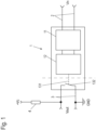
- Figure 1 shows an embodiment of a device 1 for detecting alternating voltage in a block diagram.
- the device 1 has input terminals 2 to which an alternating voltage Vin to be detected can be applied.
- the device 1 further has two potential-free output terminals 3, which are galvanically isolated from the input terminals 2, which in the Figure 1 indicated by the dashed line.
- a higher-level monitoring device can query whether the AC voltage Vin is present at the input terminals 2. Due to the galvanic isolation, the query can be performed at a voltage level that is independent of the AC voltage Vin, in particular at the level of a very low DC voltage.
- the AC voltage Vin at the input terminals 2 is usually an AC extra-low voltage with a voltage level of 60 V or more.
- the output terminals are connected to a switching element 132, symbolically represented as a switch.
- a switching element 132 symbolically represented as a switch.
- one of the output terminals 3 is coupled to a ground terminal GND and the other output terminal 3 is connected to a positive potential Vc via a pull-up resistor 4.
- This potential Vc can be provided, for example, by the higher-level monitoring device.
- the output terminals 3 form a voltage output at which a voltage Vout is applied depending on the switch position of the switching element 132. Due to the type of arrangement of the pull-up resistor 4, Vout is approximately equal to Vc when the switching element 132 is not switched and approximately equal to zero when the switching element 132 is switched on.
- the device 1 can be used, for example, to check whether a power supply line switched by a relay or contactor, a circuit breaker, a residual current device, or a load-break switch is actually live. By comparing the voltage signal Vout with a predetermined switching state of said device, correct functioning of the device can be verified.
- the device 1 operates particularly energy-efficiently in that the switching element 132 is not permanently switched when the alternating voltage Vin is applied, but with the aid of a zero-crossing detector 12 is only briefly switched on once per half-cycle of the alternating voltage Vin.
- the switching element 132 is only switched on for one millisecond (ms) or less after a zero crossing is detected.
- a pulse time parameter here the pulse start, is made dependent on a detected zero crossing.
- An alternating voltage of an assumed frequency of 50 Hz has a period of 20 ms and accordingly a zero crossing every 10 ms. If the switching element 132 is then only switched for, for example, 1 ms, only 10% of the switching energy is required for the switching element 132 compared to continuous switching.
- An input voltage converter 11 is connected upstream of the zero-crossing detector 12, which converts the alternating voltage Vin into a lower alternating voltage (or a pulsating direct voltage). This voltage is then fed to the zero-crossing detector 12. Since a phase shift can be introduced by the input voltage converter 11, the switching element 132 is not necessarily switched at the zero crossing of the alternating voltage Vin, but once per half-wave or once per period, depending on whether a zero crossing is detected during falling and rising voltage or only during either falling or rising voltage.
- the Vout signal pulses through the zero-crossing detector 12.
- the Vout signal is detected at the output terminals 3, it must be taken into account that if the Vout signal is measured for longer than half (or a full) period of the alternating voltage, it is determined whether the Vout signal is equal to zero. If the Vout signal is equal to zero at any time within a period of more than half (or a full) period, the alternating voltage Vin is present. Only if a Vout signal other than zero is detected for at least half (or a full) period can it be concluded that no alternating voltage Vin is present at the input terminals 2. If the Vout signal is evaluated as a digital signal via a microcontroller, for example, this can be easily detected programmatically.
- an RC element with a period duration adapted to the period duration of the input AC voltage Vin adjusted time constant, which smoothes the signal Vout.
- the signal Vout then decreases with the time constant to a minimum value close to zero. If the alternating voltage Vin is no longer present, the signal Vout increases with this time constant to a maximum value close to Vc.
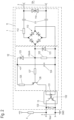
- Figure 2 shows a second embodiment of a monitoring device 1 in a more detailed circuit diagram than Figure 1 . Except for the previously mentioned RC element, the circuit structure of the Figure 2 on the embodiment of the Figure 1 The external circuit of the device 1 is Figure 2 analogous to that of the Figure 1 .
- the coupler 13 is, for example, an optocoupler, which will also be referred to below as optocoupler 13.
- the switching element 132 is a phototransistor of the optocoupler 13.
- An RC element 133 is connected in parallel with the switching path of the phototransistor. This RC element serves to smooth the output signal Vout and comprises a capacitor and a resistor in series.
- a coupler operating on a different transmission principle can also be used, for example, an inductive or capacitive coupler.
- the optocoupler 13 has a light-emitting diode (LED) as a control element 131, which switches the phototransistor, i.e., the switching path 132, on when current flows.
- the control element 131 is also referred to below as LED 131.
- the LED 131 is supplied with a pulsating operating current via a zero-crossing detector 12.
- An input voltage converter 11, which is supplied by the applied alternating voltage Vin, is connected upstream of the zero-crossing detector 12 as an input stage.
- the input voltage converter 11 is constructed in the manner of a capacitor power supply. It comprises two capacitors 111 connected in series with a series resistor 112 and a bridge rectifier 113, which are directly connected to the input terminals 2. Alternatively, instead of the combination of capacitors and resistors, an arrangement with one or more resistors without a capacitor can be used. Several resistors can be connected as a voltage divider or in a cascade. An input voltage converter constructed only with resistors is somewhat lossy, but has a high overvoltage resistance. An optional capacitor 111 connected in parallel with the input terminals 2 connected suppressor diode serves as a protection element 114 against short-term high voltage pulses at the input terminals 2.
- a Zener diode 121 and a resistor 122 are connected in parallel to the outputs of bridge rectifier 113.
- a pulsating voltage Vpuls is applied to this parallel circuit, the timing of which corresponds to consecutive half-waves of the alternating voltage Vin, with negative half-waves being "flipped up" by bridge rectifier 113.
- the capacitor 124 is connected to the LED 131 of the optocoupler 13 via a series resistor 125 and a transistor 126.
- the transistor 126 is a PNP bipolar transistor whose control input is connected via another series resistor 127 to the node at which the pulsating voltage Vpuls is applied.
- the illumination duration of LED 131 will be short compared to half the period of the alternating voltage Vin.
- a illumination duration in the range of milliseconds or less can be set.
Landscapes
- Engineering & Computer Science (AREA)
- Power Engineering (AREA)
- Physics & Mathematics (AREA)
- General Physics & Mathematics (AREA)
- Measurement Of Current Or Voltage (AREA)
- Rectifiers (AREA)
Claims (9)
- Dispositif (1) pour la détection d'une tension de courant alternatif, comprenant des branchements d'entrée (2) pour l'application d'une tension de courant alternatif à détecter (Vin) et des branchements de sortie (3) sur lesquels une application de la tension de courant alternatif (Vin) est indiquée, dans lequel les branchements d'entrée (2) et les branchements de sortie (3) sont séparés galvaniquement les uns des autres par un coupleur (13) conformé comme un optocoupleur et dans lequel une diode électroluminescente servant d'élément de commande (131) du coupleur (13) est alimentée en courant de fonctionnement par la tension de courant alternatif appliquée et un élément de commutation (132) du coupleur (13) est connecté aux branchements de sortie (3), caractérisé en ce que le dispositif (1) comprend un détecteur de passage à zéro (12) pour la tension de courant alternatif à détecter (Vin), qui alimente l'élément de commande (131) du coupleur (13) en courant de fonctionnement en impulsions, et en ce qu'un élément RC (133) est disposé en parallèle aux branchements du phototransistor de l'optocoupleur (13), de telle manière qu'il lisse de façon analogique le signal pouvant être capté sur les branchements de sortie.
- Dispositif (1) selon la revendication 1, dans lequel est monté en amont du détecteur de passage à zéro (12) un convertisseur de tension d'entrée (11) qui convertit la tension de courant alternatif (Vin) en tension de courant alternatif ou en tension de courant continu en impulsions (Vpuls) ayant une valeur de tension plus basse.
- Dispositif (1) selon la revendication 2, dans lequel le convertisseur de tension d'entrée (11) comprend un redresseur et au moins un condensateur (111) monté en amont et/ou une résistance d'amont (112) montée en amont.
- Dispositif (1) selon la revendication 3, dans lequel le redresseur des convertisseurs de tension d'entrée (11) est au moins un redresseur à pont (113).
- Dispositif (1) selon l'une des revendications 1 à 4, dans lequel le détecteur de passage à zéro (12) comprend une diode (123) et un condensateur de lissage (124) afin de former à son entrée, à partir de la tension de courant alternatif ou de la tension de courant continu en impulsions (Vpuls), une tension de courant continu (V=) pour alimenter l'élément de commande (131).
- Dispositif (1) selon l'une des revendications 1 à 5, dans lequel le détecteur de passage à zéro (12) comprend un transistor de commutation (126) dont les triangles de commutation sont montés en série avec l'élément de commande (131) et dont l'entrée de commande est couplée avec la tension de courant alternatif ou la tension de courant continu en impulsions (Vpuls) à son entrée.
- Dispositif (1) selon l'une des revendications 1 à 6, dans lequel les branchements de sortie (3) sont connectés aux branchements d'un phototransistor du coupleur (13) réalisé comme un optocoupleur.
- Procédé pour la détection d'une tension de courant alternatif, avec un dispositif qui comporte des branchements d'entrée (2) pour l'application d'une tension de courant alternatif à détecter (Vin) et des branchements de sortie (3), sur lesquels une application de la tension de courant alternatif (Vin) est indiquée, dans lequel les branchements d'entrée (2) et les branchements de sortie (3) sont séparés galvaniquement les uns des autres par un coupleur (13) et dans lequel l'élément de commande (131) du coupleur (13) est alimenté en courant de fonctionnement par la tension de courant alternatif appliquée, caractérisé en ce que l'élément de commande (131) du coupleur (13) est alimenté en courant de fonctionnement en impulsions, un paramètre de durée des impulsions étant dépendant d'un passage à zéro de la tension de courant alternatif (Vin).
- Procédé selon la revendication 8, dans lequel le paramètre de durée des impulsions est un instant de début d'une des impulsions, un instant de fin d'une des impulsions et/ou une longueur des impulsions.
Applications Claiming Priority (2)
| Application Number | Priority Date | Filing Date | Title |
|---|---|---|---|
| DE102020121643.2A DE102020121643A1 (de) | 2020-08-18 | 2020-08-18 | Kontaktüberwachung |
| PCT/EP2021/072851 WO2022038148A1 (fr) | 2020-08-18 | 2021-08-17 | Dispositif et procédé de détection de tension alternative |
Publications (2)
| Publication Number | Publication Date |
|---|---|
| EP4200623A1 EP4200623A1 (fr) | 2023-06-28 |
| EP4200623B1 true EP4200623B1 (fr) | 2025-04-23 |
Family
ID=77627116
Family Applications (1)
| Application Number | Title | Priority Date | Filing Date |
|---|---|---|---|
| EP21765622.2A Active EP4200623B1 (fr) | 2020-08-18 | 2021-08-17 | Dispositif et procédé pour détecter une tension alternative |
Country Status (4)
| Country | Link |
|---|---|
| US (1) | US20230299654A1 (fr) |
| EP (1) | EP4200623B1 (fr) |
| DE (1) | DE102020121643A1 (fr) |
| WO (1) | WO2022038148A1 (fr) |
Families Citing this family (1)
| Publication number | Priority date | Publication date | Assignee | Title |
|---|---|---|---|---|
| TWI859638B (zh) * | 2022-11-24 | 2024-10-21 | 尼克森微電子股份有限公司 | 交流電控制系統 |
Family Cites Families (9)
| Publication number | Priority date | Publication date | Assignee | Title |
|---|---|---|---|---|
| US3350574A (en) * | 1965-01-11 | 1967-10-31 | Bendix Corp | Network for converting a direct current signal into pulses having a frequency corresponding to the amplitude of the direct current signal |
| US4151464A (en) * | 1977-03-28 | 1979-04-24 | Power-Science, Inc. | Integrating voltage to frequency converter and memory decoder |
| US4229669A (en) | 1978-04-03 | 1980-10-21 | International Business Machines Corporation | Tight tolerance zero crossing detector circuit |
| US4390796A (en) * | 1981-04-15 | 1983-06-28 | Leeds & Northrup Co. | Voltage to duty cycle converter |
| US8669787B2 (en) * | 2012-05-17 | 2014-03-11 | Rockwell Automation Technologies, Inc. | Zero-crossing detector for industrial control with low heat dissipation |
| US9768697B2 (en) * | 2014-02-26 | 2017-09-19 | Infineon Technologies Austria Ag | System and method for controlling a switched mode power supply using a feedback signal |
| US9853553B2 (en) * | 2014-03-03 | 2017-12-26 | Infineon Technologies Austria Ag | Interface circuits for USB and lighting applications |
| CN105098765B (zh) * | 2014-05-19 | 2019-01-11 | 青岛海尔智能家电科技有限公司 | 一种支持多路开关的电压过零投切控制装置 |
| CN207909743U (zh) * | 2018-01-19 | 2018-09-25 | 茂硕电源科技股份有限公司 | 开关电路 |
-
2020
- 2020-08-18 DE DE102020121643.2A patent/DE102020121643A1/de active Pending
-
2021
- 2021-08-17 WO PCT/EP2021/072851 patent/WO2022038148A1/fr not_active Ceased
- 2021-08-17 EP EP21765622.2A patent/EP4200623B1/fr active Active
- 2021-08-17 US US18/041,347 patent/US20230299654A1/en active Pending
Also Published As
| Publication number | Publication date |
|---|---|
| WO2022038148A1 (fr) | 2022-02-24 |
| DE102020121643A1 (de) | 2022-02-24 |
| EP4200623A1 (fr) | 2023-06-28 |
| US20230299654A1 (en) | 2023-09-21 |
Similar Documents
| Publication | Publication Date | Title |
|---|---|---|
| EP3807661B1 (fr) | Dispositif de surveillance de commutation | |
| DE102018118329B3 (de) | Verfahren zum Nullpunktschalten eines Relais sowie Relaisschaltung | |
| EP3281022B1 (fr) | Bloc électrique ainsi que circuit de mesure et procédé de mesure pour la surveillance d'un composant du bloc électrique | |
| DE3320975C2 (de) | Elektronisches, vorzugsweise berührungslos arbeitendes Schaltgerät | |
| EP4200623B1 (fr) | Dispositif et procédé pour détecter une tension alternative | |
| EP0935758B1 (fr) | Procede et circuit pour la surveillance d'une valeur seuil d'amplitude definie de signaux sous forme de tension alternative | |
| DE102018100974B4 (de) | Schaltungsanordnung | |
| EP2770641B1 (fr) | Dispositif d'exploitation de signaux d'entrée électriques | |
| DE19807517A1 (de) | 2-Drahtschalter | |
| EP1109177B1 (fr) | Procédé pour commuter une charge | |
| DE10214738B4 (de) | Falschanschlusserkennungsschaltung und Verfahren zur Erkennung eines Falschanschlusses | |
| EP1970717A2 (fr) | Circuit et procédé d'alimentation en tension de feuilles électroluminescentes | |
| EP0638812A2 (fr) | Dispositif de contrôle de défauts électriques dans un déclencheur d'un appareillage électrique | |
| EP0855035B1 (fr) | Procede permettant de faire fonctionner un circuit d'entree et circuit d'entree correspondant | |
| DE19820965A1 (de) | Meßeinrichtung zur verlustarmen Messung der Netzimpedanz | |
| DE19936214B4 (de) | Verfahren zur Bestimmung eines Wiederaufschaltmoments für eine Versorgungs-Netzspannung für einen Netzabkoppler | |
| DE10013928C2 (de) | Verfahren zum Schalten einer Last | |
| DE19958039C2 (de) | Vorrichtung und Verfahren zur Vermeidung von Strom- und Spannungsspitzen | |
| EP3149834A1 (fr) | Appareil d'alimentation en énergie à transitions entre les modes marche et attente dépendantes du courant de sortie | |
| EP0843505A1 (fr) | Ballast électronique pour au moins une lampe à décharge | |
| DE19748632A1 (de) | Verfahren und Schaltungsanordnung zur Eingangsspannungsüberwachung von Netzteilen mit Wechselspannungsversorgung | |
| DE29803115U1 (de) | 2-Drahtschalter | |
| WO2000063930A1 (fr) | Circuit d'entree pour signaux de courant alternatif a intensite relativement elevee a surveiller | |
| DE19847179A1 (de) | Überwachung einer galvanisch getrennten Spannung | |
| DD288020A5 (de) | Schaltungsanordnung zur ununterbrochenen stromversorgung elektronischer baugruppen mit startfunktion und informationserkennung |
Legal Events
| Date | Code | Title | Description |
|---|---|---|---|
| STAA | Information on the status of an ep patent application or granted ep patent |
Free format text: STATUS: UNKNOWN |
|
| STAA | Information on the status of an ep patent application or granted ep patent |
Free format text: STATUS: THE INTERNATIONAL PUBLICATION HAS BEEN MADE |
|
| PUAI | Public reference made under article 153(3) epc to a published international application that has entered the european phase |
Free format text: ORIGINAL CODE: 0009012 |
|
| STAA | Information on the status of an ep patent application or granted ep patent |
Free format text: STATUS: REQUEST FOR EXAMINATION WAS MADE |
|
| 17P | Request for examination filed |
Effective date: 20230216 |
|
| AK | Designated contracting states |
Kind code of ref document: A1 Designated state(s): AL AT BE BG CH CY CZ DE DK EE ES FI FR GB GR HR HU IE IS IT LI LT LU LV MC MK MT NL NO PL PT RO RS SE SI SK SM TR |
|
| DAV | Request for validation of the european patent (deleted) | ||
| DAX | Request for extension of the european patent (deleted) | ||
| GRAP | Despatch of communication of intention to grant a patent |
Free format text: ORIGINAL CODE: EPIDOSNIGR1 |
|
| STAA | Information on the status of an ep patent application or granted ep patent |
Free format text: STATUS: GRANT OF PATENT IS INTENDED |
|
| RIC1 | Information provided on ipc code assigned before grant |
Ipc: G01R 19/175 20060101AFI20241216BHEP |
|
| INTG | Intention to grant announced |
Effective date: 20250113 |
|
| GRAS | Grant fee paid |
Free format text: ORIGINAL CODE: EPIDOSNIGR3 |
|
| P01 | Opt-out of the competence of the unified patent court (upc) registered |
Free format text: CASE NUMBER: APP_7261/2025 Effective date: 20250212 |
|
| GRAA | (expected) grant |
Free format text: ORIGINAL CODE: 0009210 |
|
| STAA | Information on the status of an ep patent application or granted ep patent |
Free format text: STATUS: THE PATENT HAS BEEN GRANTED |
|
| AK | Designated contracting states |
Kind code of ref document: B1 Designated state(s): AL AT BE BG CH CY CZ DE DK EE ES FI FR GB GR HR HU IE IS IT LI LT LU LV MC MK MT NL NO PL PT RO RS SE SI SK SM TR |
|
| REG | Reference to a national code |
Ref country code: GB Ref legal event code: FG4D Free format text: NOT ENGLISH |
|
| REG | Reference to a national code |
Ref country code: CH Ref legal event code: EP |
|
| REG | Reference to a national code |
Ref country code: DE Ref legal event code: R096 Ref document number: 502021007297 Country of ref document: DE |
|
| REG | Reference to a national code |
Ref country code: IE Ref legal event code: FG4D Free format text: LANGUAGE OF EP DOCUMENT: GERMAN |
|
| REG | Reference to a national code |
Ref country code: NL Ref legal event code: MP Effective date: 20250423 |
|
| PG25 | Lapsed in a contracting state [announced via postgrant information from national office to epo] |
Ref country code: NL Free format text: LAPSE BECAUSE OF FAILURE TO SUBMIT A TRANSLATION OF THE DESCRIPTION OR TO PAY THE FEE WITHIN THE PRESCRIBED TIME-LIMIT Effective date: 20250423 |
|
| PG25 | Lapsed in a contracting state [announced via postgrant information from national office to epo] |
Ref country code: FI Free format text: LAPSE BECAUSE OF FAILURE TO SUBMIT A TRANSLATION OF THE DESCRIPTION OR TO PAY THE FEE WITHIN THE PRESCRIBED TIME-LIMIT Effective date: 20250423 Ref country code: PT Free format text: LAPSE BECAUSE OF FAILURE TO SUBMIT A TRANSLATION OF THE DESCRIPTION OR TO PAY THE FEE WITHIN THE PRESCRIBED TIME-LIMIT Effective date: 20250825 Ref country code: ES Free format text: LAPSE BECAUSE OF FAILURE TO SUBMIT A TRANSLATION OF THE DESCRIPTION OR TO PAY THE FEE WITHIN THE PRESCRIBED TIME-LIMIT Effective date: 20250423 |
|
| PGFP | Annual fee paid to national office [announced via postgrant information from national office to epo] |
Ref country code: DE Payment date: 20250820 Year of fee payment: 5 |
|
| REG | Reference to a national code |
Ref country code: LT Ref legal event code: MG9D |
|
| PG25 | Lapsed in a contracting state [announced via postgrant information from national office to epo] |
Ref country code: GR Free format text: LAPSE BECAUSE OF FAILURE TO SUBMIT A TRANSLATION OF THE DESCRIPTION OR TO PAY THE FEE WITHIN THE PRESCRIBED TIME-LIMIT Effective date: 20250724 Ref country code: NO Free format text: LAPSE BECAUSE OF FAILURE TO SUBMIT A TRANSLATION OF THE DESCRIPTION OR TO PAY THE FEE WITHIN THE PRESCRIBED TIME-LIMIT Effective date: 20250723 |
|
| PG25 | Lapsed in a contracting state [announced via postgrant information from national office to epo] |
Ref country code: PL Free format text: LAPSE BECAUSE OF FAILURE TO SUBMIT A TRANSLATION OF THE DESCRIPTION OR TO PAY THE FEE WITHIN THE PRESCRIBED TIME-LIMIT Effective date: 20250423 |
|
| PG25 | Lapsed in a contracting state [announced via postgrant information from national office to epo] |
Ref country code: BG Free format text: LAPSE BECAUSE OF FAILURE TO SUBMIT A TRANSLATION OF THE DESCRIPTION OR TO PAY THE FEE WITHIN THE PRESCRIBED TIME-LIMIT Effective date: 20250423 |
|
| PG25 | Lapsed in a contracting state [announced via postgrant information from national office to epo] |
Ref country code: HR Free format text: LAPSE BECAUSE OF FAILURE TO SUBMIT A TRANSLATION OF THE DESCRIPTION OR TO PAY THE FEE WITHIN THE PRESCRIBED TIME-LIMIT Effective date: 20250423 |
|
| PGFP | Annual fee paid to national office [announced via postgrant information from national office to epo] |
Ref country code: AT Payment date: 20251020 Year of fee payment: 5 |
|
| PG25 | Lapsed in a contracting state [announced via postgrant information from national office to epo] |
Ref country code: RS Free format text: LAPSE BECAUSE OF FAILURE TO SUBMIT A TRANSLATION OF THE DESCRIPTION OR TO PAY THE FEE WITHIN THE PRESCRIBED TIME-LIMIT Effective date: 20250723 |
|
| PG25 | Lapsed in a contracting state [announced via postgrant information from national office to epo] |
Ref country code: IS Free format text: LAPSE BECAUSE OF FAILURE TO SUBMIT A TRANSLATION OF THE DESCRIPTION OR TO PAY THE FEE WITHIN THE PRESCRIBED TIME-LIMIT Effective date: 20250823 |
|
| PG25 | Lapsed in a contracting state [announced via postgrant information from national office to epo] |
Ref country code: LV Free format text: LAPSE BECAUSE OF FAILURE TO SUBMIT A TRANSLATION OF THE DESCRIPTION OR TO PAY THE FEE WITHIN THE PRESCRIBED TIME-LIMIT Effective date: 20250423 |
|
| PG25 | Lapsed in a contracting state [announced via postgrant information from national office to epo] |
Ref country code: SM Free format text: LAPSE BECAUSE OF FAILURE TO SUBMIT A TRANSLATION OF THE DESCRIPTION OR TO PAY THE FEE WITHIN THE PRESCRIBED TIME-LIMIT Effective date: 20250423 Ref country code: DK Free format text: LAPSE BECAUSE OF FAILURE TO SUBMIT A TRANSLATION OF THE DESCRIPTION OR TO PAY THE FEE WITHIN THE PRESCRIBED TIME-LIMIT Effective date: 20250423 |
|
| PG25 | Lapsed in a contracting state [announced via postgrant information from national office to epo] |
Ref country code: CZ Free format text: LAPSE BECAUSE OF FAILURE TO SUBMIT A TRANSLATION OF THE DESCRIPTION OR TO PAY THE FEE WITHIN THE PRESCRIBED TIME-LIMIT Effective date: 20250423 |
|
| PG25 | Lapsed in a contracting state [announced via postgrant information from national office to epo] |
Ref country code: EE Free format text: LAPSE BECAUSE OF FAILURE TO SUBMIT A TRANSLATION OF THE DESCRIPTION OR TO PAY THE FEE WITHIN THE PRESCRIBED TIME-LIMIT Effective date: 20250423 |
|
| REG | Reference to a national code |
Ref country code: DE Ref legal event code: R097 Ref document number: 502021007297 Country of ref document: DE |
|
| PG25 | Lapsed in a contracting state [announced via postgrant information from national office to epo] |
Ref country code: SK Free format text: LAPSE BECAUSE OF FAILURE TO SUBMIT A TRANSLATION OF THE DESCRIPTION OR TO PAY THE FEE WITHIN THE PRESCRIBED TIME-LIMIT Effective date: 20250423 |
|
| PG25 | Lapsed in a contracting state [announced via postgrant information from national office to epo] |
Ref country code: IT Free format text: LAPSE BECAUSE OF FAILURE TO SUBMIT A TRANSLATION OF THE DESCRIPTION OR TO PAY THE FEE WITHIN THE PRESCRIBED TIME-LIMIT Effective date: 20250423 |
|
| PLBE | No opposition filed within time limit |
Free format text: ORIGINAL CODE: 0009261 |
|
| STAA | Information on the status of an ep patent application or granted ep patent |
Free format text: STATUS: NO OPPOSITION FILED WITHIN TIME LIMIT |
|
| REG | Reference to a national code |
Ref country code: CH Ref legal event code: L10 Free format text: ST27 STATUS EVENT CODE: U-0-0-L10-L00 (AS PROVIDED BY THE NATIONAL OFFICE) Effective date: 20260304 |
|
| PG25 | Lapsed in a contracting state [announced via postgrant information from national office to epo] |
Ref country code: RO Free format text: LAPSE BECAUSE OF FAILURE TO SUBMIT A TRANSLATION OF THE DESCRIPTION OR TO PAY THE FEE WITHIN THE PRESCRIBED TIME-LIMIT Effective date: 20250423 |
|
| REG | Reference to a national code |
Ref country code: CH Ref legal event code: H13 Free format text: ST27 STATUS EVENT CODE: U-0-0-H10-H13 (AS PROVIDED BY THE NATIONAL OFFICE) Effective date: 20260324 |