EP4200623B1 - Vorrichtung und verfahren zur detektion von wechselspannung - Google Patents
Vorrichtung und verfahren zur detektion von wechselspannung Download PDFInfo
- Publication number
- EP4200623B1 EP4200623B1 EP21765622.2A EP21765622A EP4200623B1 EP 4200623 B1 EP4200623 B1 EP 4200623B1 EP 21765622 A EP21765622 A EP 21765622A EP 4200623 B1 EP4200623 B1 EP 4200623B1
- Authority
- EP
- European Patent Office
- Prior art keywords
- voltage
- alternating voltage
- coupler
- input
- zero
- Prior art date
- Legal status (The legal status is an assumption and is not a legal conclusion. Google has not performed a legal analysis and makes no representation as to the accuracy of the status listed.)
- Active
Links
Images
Classifications
-
- G—PHYSICS
- G01—MEASURING; TESTING
- G01R—MEASURING ELECTRIC VARIABLES; MEASURING MAGNETIC VARIABLES
- G01R19/00—Arrangements for measuring currents or voltages or for indicating presence or sign thereof
- G01R19/175—Indicating the instants of passage of current or voltage through a given value, e.g. passage through zero
-
- H—ELECTRICITY
- H02—GENERATION; CONVERSION OR DISTRIBUTION OF ELECTRIC POWER
- H02M—APPARATUS FOR CONVERSION BETWEEN AC AND AC, BETWEEN AC AND DC, OR BETWEEN DC AND DC, AND FOR USE WITH MAINS OR SIMILAR POWER SUPPLY SYSTEMS; CONVERSION OF DC OR AC INPUT POWER INTO SURGE OUTPUT POWER; CONTROL OR REGULATION THEREOF
- H02M1/00—Details of apparatus for conversion
- H02M1/0003—Details of control, feedback or regulation circuits
- H02M1/0016—Control circuits providing compensation of output voltage deviations using feedforward of disturbance parameters
-
- H—ELECTRICITY
- H02—GENERATION; CONVERSION OR DISTRIBUTION OF ELECTRIC POWER
- H02M—APPARATUS FOR CONVERSION BETWEEN AC AND AC, BETWEEN AC AND DC, OR BETWEEN DC AND DC, AND FOR USE WITH MAINS OR SIMILAR POWER SUPPLY SYSTEMS; CONVERSION OF DC OR AC INPUT POWER INTO SURGE OUTPUT POWER; CONTROL OR REGULATION THEREOF
- H02M1/00—Details of apparatus for conversion
- H02M1/08—Circuits specially adapted for the generation of control voltages for semiconductor devices incorporated in static converters
- H02M1/083—Circuits specially adapted for the generation of control voltages for semiconductor devices incorporated in static converters for the ignition at the zero crossing of the voltage or the current
-
- H—ELECTRICITY
- H02—GENERATION; CONVERSION OR DISTRIBUTION OF ELECTRIC POWER
- H02M—APPARATUS FOR CONVERSION BETWEEN AC AND AC, BETWEEN AC AND DC, OR BETWEEN DC AND DC, AND FOR USE WITH MAINS OR SIMILAR POWER SUPPLY SYSTEMS; CONVERSION OF DC OR AC INPUT POWER INTO SURGE OUTPUT POWER; CONTROL OR REGULATION THEREOF
- H02M3/00—Conversion of DC power input into DC power output
- H02M3/02—Conversion of DC power input into DC power output without intermediate conversion into AC
- H02M3/04—Conversion of DC power input into DC power output without intermediate conversion into AC by static converters
- H02M3/10—Conversion of DC power input into DC power output without intermediate conversion into AC by static converters using discharge tubes with control electrode or semiconductor devices with control electrode
- H02M3/145—Conversion of DC power input into DC power output without intermediate conversion into AC by static converters using discharge tubes with control electrode or semiconductor devices with control electrode using devices of a triode or transistor type requiring continuous application of a control signal
- H02M3/155—Conversion of DC power input into DC power output without intermediate conversion into AC by static converters using discharge tubes with control electrode or semiconductor devices with control electrode using devices of a triode or transistor type requiring continuous application of a control signal using semiconductor devices only
- H02M3/156—Conversion of DC power input into DC power output without intermediate conversion into AC by static converters using discharge tubes with control electrode or semiconductor devices with control electrode using devices of a triode or transistor type requiring continuous application of a control signal using semiconductor devices only with automatic control of output voltage or current, e.g. switching regulators
- H02M3/158—Conversion of DC power input into DC power output without intermediate conversion into AC by static converters using discharge tubes with control electrode or semiconductor devices with control electrode using devices of a triode or transistor type requiring continuous application of a control signal using semiconductor devices only with automatic control of output voltage or current, e.g. switching regulators including plural semiconductor devices as final control devices for a single load
Definitions
- the invention relates to a device for detecting alternating voltage, comprising input terminals for applying an alternating voltage to be detected and output terminals at which the presence of the alternating voltage is indicated.
- the input terminals and the output terminals are galvanically isolated from one another by a coupler, wherein a control element of the coupler is supplied with operating current by the applied alternating voltage, and a switching element of the coupler is connected to the output terminals.
- the invention further relates to a method for detecting alternating voltage, which can be carried out in particular with the aforementioned device.
- Such devices are used to check for the presence of alternating voltage at specific nodes in an electrical installation, for example, by reading the output connections from a higher-level monitoring device.
- a common application is to determine the correct functioning of relays or contactors, circuit breakers, residual current devices, or load break switches by detecting the presence of alternating voltage (output side) at switching contacts and comparing it with the specified switching state of the device being tested.
- the AC voltage to be detected is usually a low voltage with a voltage of more than 60 V, such as a lighting mains voltage.
- the higher-level monitoring device can be, for example, an industrial automation system used for monitoring or control purposes.
- the monitoring device can also be a gateway or a data logger, which then only performs monitoring.
- the inputs of such monitoring devices are usually designed to detect a switching signal or a protective extra-low voltage, for example 12 volts (V) or 24 V.
- the aforementioned device for detecting alternating voltage transmits the information about the presence of alternating voltage in the form of a galvanically isolated switching signal to the monitoring device.
- the coupler is usually an optocoupler with a light-emitting diode (LED) as the control element for galvanic isolation.
- the optocoupler is supplied with operating current from the applied alternating voltage so that the switching element of the optocoupler, usually a phototransistor, becomes conductive.
- a series circuit comprising a rectifier diode and a series resistor can be used to drive the optocoupler's LED using the AC voltage.
- the series resistor can be an ohmic resistor and/or a capacitor with its AC resistance. While this results in a very simple design, the disadvantage is that the LED's series resistor for the optocoupler dissipates power in the range of several tens to several hundred milliwatts (mW), which leads to energy-inefficient operation of the device. Furthermore, such an arrangement also detects a DC voltage on the input side, which is not desirable in all applications.
- the document EP 2 665 182 A2 describes a zero-crossing detector with input terminals for applying an alternating voltage and with output terminals galvanically isolated by means of an optocoupler.
- a device according to the invention of the type mentioned at the outset has a zero-crossing detector for the alternating voltage to be detected, which zero-crossing detector supplies the control element of the coupler with the operating current in pulsed form.
- the device operates particularly energy-efficiently in that the switching element is not permanently energized when the alternating voltage is applied, but is only energized for a short time with the help of the zero-crossing detector. Furthermore, in this way only alternating current is advantageously detected, not direct current.
- the switching element is only switched for a period of 10% of the half-wave of the alternating voltage following the zero crossing, this results in a saving of 90% of the energy required to control the switching element compared to continuous control of the switching element.
- the galvanically isolating coupler can operate inductively, capacitively, or optically, and in particular can be formed by an optocoupler.
- the control element in this case is a light-emitting diode.
- an input voltage converter is connected upstream of the zero-crossing detector, which converts the alternating voltage into an alternating voltage or pulsed direct voltage with a lower voltage value.
- the zero-crossing detector can be constructed with less effort at lower voltages.
- the input voltage converter can have a rectifier with at least one upstream capacitor and/or upstream series resistor.
- the aforementioned combination of rectifier, capacitor, and series resistor allows the construction of a cost-effective voltage converter with relatively low power losses.
- At least one bridge rectifier is preferably used as the rectifier.
- the zero-crossing detector has a diode and a smoothing capacitor to generate a DC voltage from the AC voltage or the pulsed DC voltage at its input to supply the control element.
- a switching transistor is connected in series with the control element via its switching path, with a control input of the switching transistor being coupled to the AC voltage or the pulsed DC voltage at the input of the zero-voltage converter. The switching transistor is controlled such that it only switches on in the zero-crossing region.
- the device its output terminals are connected to the terminals of a phototransistor of the coupler designed as an optocoupler.
- the (pulsating) switching state of the phototransistor can then be queried at the output terminals. It should be noted that the switching state is observed over a period of at least half (or a full) period of the alternating voltage in order to determine whether alternating voltage is present at the input terminals. With a digital evaluation of the switching state of the phototransistor This can easily be implemented programmatically using a microcontroller, for example.
- an RC element is arranged parallel to the terminals of the phototransistor of the optocoupler.
- the RC element smooths the signal available at the output terminals in an analog manner, making it easy to determine whether an AC input voltage is present or not, even without evaluation by a microcontroller.
- other timing elements analog or digital
- a method according to the invention is used to detect alternating voltage using a device that has input terminals for applying an alternating voltage to be detected and output terminals at which the presence of the alternating voltage is indicated.
- the input terminals and the output terminals are galvanically isolated from one another by a coupler, wherein a control element of the coupler is supplied with operating current from the applied alternating voltage and a switching element of the coupler is connected to the output terminals.
- the method is characterized in that the control element of the coupler is supplied with the operating current in pulsed form, wherein a pulse time parameter is dependent on a zero crossing of the alternating voltage.
- a pulse time parameter is understood to be a start time, an end time and/or a pulse length. The method can be carried out, for example, using the device described above. The advantages stated in connection with the device result.
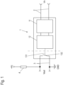
- Figure 1 shows an embodiment of a device 1 for detecting alternating voltage in a block diagram.
- the device 1 has input terminals 2 to which an alternating voltage Vin to be detected can be applied.
- the device 1 further has two potential-free output terminals 3, which are galvanically isolated from the input terminals 2, which in the Figure 1 indicated by the dashed line.
- a higher-level monitoring device can query whether the AC voltage Vin is present at the input terminals 2. Due to the galvanic isolation, the query can be performed at a voltage level that is independent of the AC voltage Vin, in particular at the level of a very low DC voltage.
- the AC voltage Vin at the input terminals 2 is usually an AC extra-low voltage with a voltage level of 60 V or more.
- the output terminals are connected to a switching element 132, symbolically represented as a switch.
- a switching element 132 symbolically represented as a switch.
- one of the output terminals 3 is coupled to a ground terminal GND and the other output terminal 3 is connected to a positive potential Vc via a pull-up resistor 4.
- This potential Vc can be provided, for example, by the higher-level monitoring device.
- the output terminals 3 form a voltage output at which a voltage Vout is applied depending on the switch position of the switching element 132. Due to the type of arrangement of the pull-up resistor 4, Vout is approximately equal to Vc when the switching element 132 is not switched and approximately equal to zero when the switching element 132 is switched on.
- the device 1 can be used, for example, to check whether a power supply line switched by a relay or contactor, a circuit breaker, a residual current device, or a load-break switch is actually live. By comparing the voltage signal Vout with a predetermined switching state of said device, correct functioning of the device can be verified.
- the device 1 operates particularly energy-efficiently in that the switching element 132 is not permanently switched when the alternating voltage Vin is applied, but with the aid of a zero-crossing detector 12 is only briefly switched on once per half-cycle of the alternating voltage Vin.
- the switching element 132 is only switched on for one millisecond (ms) or less after a zero crossing is detected.
- a pulse time parameter here the pulse start, is made dependent on a detected zero crossing.
- An alternating voltage of an assumed frequency of 50 Hz has a period of 20 ms and accordingly a zero crossing every 10 ms. If the switching element 132 is then only switched for, for example, 1 ms, only 10% of the switching energy is required for the switching element 132 compared to continuous switching.
- An input voltage converter 11 is connected upstream of the zero-crossing detector 12, which converts the alternating voltage Vin into a lower alternating voltage (or a pulsating direct voltage). This voltage is then fed to the zero-crossing detector 12. Since a phase shift can be introduced by the input voltage converter 11, the switching element 132 is not necessarily switched at the zero crossing of the alternating voltage Vin, but once per half-wave or once per period, depending on whether a zero crossing is detected during falling and rising voltage or only during either falling or rising voltage.
- the Vout signal pulses through the zero-crossing detector 12.
- the Vout signal is detected at the output terminals 3, it must be taken into account that if the Vout signal is measured for longer than half (or a full) period of the alternating voltage, it is determined whether the Vout signal is equal to zero. If the Vout signal is equal to zero at any time within a period of more than half (or a full) period, the alternating voltage Vin is present. Only if a Vout signal other than zero is detected for at least half (or a full) period can it be concluded that no alternating voltage Vin is present at the input terminals 2. If the Vout signal is evaluated as a digital signal via a microcontroller, for example, this can be easily detected programmatically.
- an RC element with a period duration adapted to the period duration of the input AC voltage Vin adjusted time constant, which smoothes the signal Vout.
- the signal Vout then decreases with the time constant to a minimum value close to zero. If the alternating voltage Vin is no longer present, the signal Vout increases with this time constant to a maximum value close to Vc.
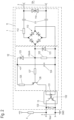
- Figure 2 shows a second embodiment of a monitoring device 1 in a more detailed circuit diagram than Figure 1 . Except for the previously mentioned RC element, the circuit structure of the Figure 2 on the embodiment of the Figure 1 The external circuit of the device 1 is Figure 2 analogous to that of the Figure 1 .
- the coupler 13 is, for example, an optocoupler, which will also be referred to below as optocoupler 13.
- the switching element 132 is a phototransistor of the optocoupler 13.
- An RC element 133 is connected in parallel with the switching path of the phototransistor. This RC element serves to smooth the output signal Vout and comprises a capacitor and a resistor in series.
- a coupler operating on a different transmission principle can also be used, for example, an inductive or capacitive coupler.
- the optocoupler 13 has a light-emitting diode (LED) as a control element 131, which switches the phototransistor, i.e., the switching path 132, on when current flows.
- the control element 131 is also referred to below as LED 131.
- the LED 131 is supplied with a pulsating operating current via a zero-crossing detector 12.
- An input voltage converter 11, which is supplied by the applied alternating voltage Vin, is connected upstream of the zero-crossing detector 12 as an input stage.
- the input voltage converter 11 is constructed in the manner of a capacitor power supply. It comprises two capacitors 111 connected in series with a series resistor 112 and a bridge rectifier 113, which are directly connected to the input terminals 2. Alternatively, instead of the combination of capacitors and resistors, an arrangement with one or more resistors without a capacitor can be used. Several resistors can be connected as a voltage divider or in a cascade. An input voltage converter constructed only with resistors is somewhat lossy, but has a high overvoltage resistance. An optional capacitor 111 connected in parallel with the input terminals 2 connected suppressor diode serves as a protection element 114 against short-term high voltage pulses at the input terminals 2.
- a Zener diode 121 and a resistor 122 are connected in parallel to the outputs of bridge rectifier 113.
- a pulsating voltage Vpuls is applied to this parallel circuit, the timing of which corresponds to consecutive half-waves of the alternating voltage Vin, with negative half-waves being "flipped up" by bridge rectifier 113.
- the capacitor 124 is connected to the LED 131 of the optocoupler 13 via a series resistor 125 and a transistor 126.
- the transistor 126 is a PNP bipolar transistor whose control input is connected via another series resistor 127 to the node at which the pulsating voltage Vpuls is applied.
- the illumination duration of LED 131 will be short compared to half the period of the alternating voltage Vin.
- a illumination duration in the range of milliseconds or less can be set.
Landscapes
- Engineering & Computer Science (AREA)
- Power Engineering (AREA)
- Physics & Mathematics (AREA)
- General Physics & Mathematics (AREA)
- Measurement Of Current Or Voltage (AREA)
- Rectifiers (AREA)
Description
- Die Erfindung betrifft eine Vorrichtung zur Detektion von Wechselspannung, aufweisend Eingangsanschlüsse zum Anlegen einer zu detektierenden Wechselspannung und Ausgangsanschlüssen, an denen ein Anliegen der Wechselspannung angezeigt wird. Die Eingangsanschlüsse und die Ausgangsanschlüsse sind dabei durch einen Koppler galvanisch voneinander getrennt, wobei ein Steuerelement des Kopplers von der angelegten Wechselspannung mit Betriebsstrom versorgt wird und ein Schaltelement des Kopplers mit den Ausgangsanschlüssen verbunden ist. Die Erfindung betrifft weiter ein Verfahren zur Detektion von Wechselspannung, das insbesondere mit der genannten Vorrichtung durchführbar ist.
- Derartige Vorrichtungen werden genutzt, um in einer elektrischen Installation das Vorhandensein von Wechselspannung an bestimmten Knoten dieser Installation überprüfen zu können, indem die Ausgangsanschlüsse z.B. von einer übergeordneten Überwachungseinrichtung ausgelesen werden. Eine häufige Anwendung ist es, die korrekte Funktionsweise von z.B. Relais bzw. Schützen, Leitungsschutzschaltern, Fehlerstromschutzeinrichtungen oder Lasttrennschaltern zu ermitteln, indem das Vorhandensein der Wechselspannung (ausgangsseitig) an Schaltkontakten detektiert wird und mit dem vorgegebenen Schaltzustand des überprüften Geräts verglichen wird.
- Die zu detektierende Wechselspannung ist in der Regel eine Kleinspannung mit einer Spannung von mehr als 60 V, beispielsweise eine Lichtnetz-Spannung. Die übergeordnete Überwachungseinrichtung kann zum Beispiel eine industrielle Automatisierungsanlage sein, die zu Monitoring- oder Steuerungszwecken eingesetzt wird. Die Überwachungseinrichtung kann auch ein Gateway oder ein Datenlogger sein, über das oder den dann nur ein Monitoring erfolgt.
- Die Eingänge einer solcher Überwachungseinrichtungen sind in der Regel dazu eingerichtet, ein Schaltsignal zu erfassen oder eine Schutzkleinspannung, zum Beispiel 12 Volt (V) oder 24 V.
- Die eingangs genannte Vorrichtung zur Detektion von Wechselspannung gibt die Information über das Vorhandensein der Wechselspannung in Form eines Schaltsignals galvanisch getrennt an die Überwachungseinrichtung weiter, wobei als Koppler in der Regel ein Optokoppler mit einer Leuchtdiode (LED) als Steuerelement zur galvanischen Trennung eingesetzt wird. Die Leuchtdiode des Optokopplers wird dazu von der anliegenden Wechselspannung mit Betriebsstrom versorgt, so dass das Schaltelement des Optokopplers, üblicherweise ein Fototransistor, leitend wird.
- In einer einfachsten Ausgestaltung kann eine Serienschaltung aus Gleichrichterdiode und einem Vorwiderstand verwendet werden, um die LED des Optokopplers durch die Wechselspannung zu betreiben. Als Vorwiderstand kann ein ohmscher Widerstand und/oder ein Kondensator mit seinem Wechselstromwiderstand dienen. Zwar wird so ein sehr einfacher Aufbau erzielt, nachteilig fällt jedoch an dem Vorwiderstand der LED für den Optokoppler eine Verlustleistung im Bereich von einigen 10 bis einigen 100 Milliwatt (mW) an, die zu einem energieineffizienten Betrieb der Vorrichtung führt. Zudem detektiert eine derartige Anordnung auch eine eingangsseitige Gleichspannung, was nicht in allen Anwendungsfällen gewünscht ist.
- Das Dokument
EP 2 665 182 A2 beschreibt einen Nulldurchgangsdetektor mit Eingangsanschlüssen zum Anlegen einer Wechselspannung und mit mittels eines Optokopplers galvanisch getrennten Ausgangsanschlüssen. - Es ist daher eine Aufgabe der vorliegenden Erfindung, eine Vorrichtung und ein Verfahren zur Detektion von Wechselspannung der eingangs genannten Art zu schaffen, die bei einfachem Aufbau und robuster Funktionsweise möglichst energieeffizient mit geringen Verlustleistungen arbeiten und selektiv Wechselspannung erkennen.
- Diese Aufgabe wird durch eine Vorrichtung und ein Verfahren mit den jeweiligen Merkmalen der unabhängigen Ansprüche gelöst. Vorteilhafte Ausgestaltungen und Weiterbildungen sind Gegenstand der abhängigen Ansprüche. Eine erfindungsgemäße Vorrichtung der eingangs genannten Art weist einen Nulldurchgangsdetektor für die zu detektierende Wechselspannung auf, der das Steuerelement des Kopplers gepulst mit dem Betriebsstrom versorgt. Erfindungsgemäß arbeitet die Vorrichtung besonders energieeffizient, indem das Schaltelement beim Anliegen der Wechselspannung nicht permanent bestromt ist, sondern mithilfe des Nulldurchgangsdetektors nur kurzzeitig zeitweise bestromt wird. Zudem wird vorteilhaft auf diese Weise nur Wechselstrom detektiert, nicht Gleichstrom. Wenn beispielsweise nach Detektion eines Nulldurchgangs das Schaltelement nur für einen Zeitraum von 10 % der sich an den Nulldurchgang anschließenden Halbwelle der Wechselspannung geschaltet wird, resultiert dieses in einer Ersparnis von 90 % der für das Ansteuern des Schaltelements notwendigen Energie gegenüber einem dauerhaften Ansteuern des Schaltelements.
- Beim Verfahren gemäß Anspruch 8 kann der galvanisch trennende Koppler induktiv, kapazitiv oder optisch arbeiten, und insbesondere durch einen Optokoppler gebildet sein. Das Steuerelement ist in dem Fall eine Leuchtdiode.
- In einer vorteilhaften Ausgestaltung der Vorrichtung ist dem Nulldurchgangsdetektor ein Eingangsspannungswandler vorgeschaltet, der die Wechselspannung in eine Wechselspannung oder gepulste Gleichspannung mit kleinerem Spannungswert wandelt. Der Nulldurchgangsdetektor lässt sich bei kleinerer Spannung mit geringerem Aufwand aufbauen. Der Eingangsspannungswandler kann einen Gleichrichter mit mindestens einem vorgeschalteten Kondensator und/oder vorgeschaltetem Vorwiderstand aufweisen. Insbesondere durch die genannte Kombination von Gleichrichter, Kondensator und Vorwiderstand lässt sich ein kostengünstiger Spannungswandler mit relativ geringen Verlustleistungen aufbauen. Als Gleichrichter findet dabei bevorzugt mindestens ein Brückengleichrichter Verwendung.
- In einer weiteren vorteilhaften Ausgestaltung der Vorrichtung weist der Nulldurchgangsdetektor eine Diode und einen Glättungskondensator auf, um aus der Wechselspannung oder der gepulsten Gleichspannung an seinem Eingang eine Gleichspannung zur Versorgung des Steuerelements zu bilden. Ein Schalttransistor ist mit seiner Schaltstrecke mit dem Steuerelement serienverschaltet, wobei ein Steuereingang des Schalttransistors mit der Wechselspannung oder der gepulsten Gleichspannung am Eingang des Nullspannungswandlers gekoppelt ist. Der Schalttransistor wird dabei so angesteuert, dass er nur im Bereich des Nulldurchgangs durchschaltet.
- In einer weiteren vorteilhaften Ausgestaltung der Vorrichtung sind dessen Ausgangsanschlüsse mit den Anschlüssen eines Fototransistors des als Optokoppler ausgeführten Kopplers verbunden. Der (pulsierende) Schaltzustand des Fototransistors kann dann an den Ausgangsanschlüssen abgefragt werden. Dabei ist zu berücksichtigen, dass der Schaltzustand über einen Zeitraum von mindestens einer halben (oder ganzen) Periodendauer der Wechselspannung betrachtet wird, um zu ermitteln, ob Wechselspannung an den Eingangsanschlüssen anliegt. Bei einer digitalen Auswertung des Schaltzustands des Fototransistors über zum Beispiel einen Mikrocontroller kann dieses leicht programmgesteuert umgesetzt werden.
- Bei der Vorrichtung gemäß Anspruch 1 ist parallel zu den Anschlüssen des Fototransistors des Optokopplers ein RC-Glied angeordnet.
- Durch das RC-Glied wird das an den Ausgangsanschlüssen abgreifbare Signal analog geglättet, wodurch auch ohne Auswertung durch einen Mikrocontroller leicht geschlossen werden kann, ob eine Eingangswechselspannung anliegt oder nicht. In alternativen Ausgestaltungen des Verfahrens können andere Zeitglieder (analog oder digital arbeitende) genutzt werden, um an den Ausgangsanschlüssen ein Signal bereitzustellen, das möglichst konstant einen bestimmten Pegel aufweist, wenn an den Eingangsanschlüssen Wechselspannung anliegt, und das einen davon abweichenden Pegel aufweist, wenn an den Eingangsanschlüssen keine Wechselspannung anliegt.
- Ein erfindungsgemäßes Verfahren dient zur Detektion von Wechselspannung mit einer Vorrichtung, die Eingangsanschlüsse zum Anlegen einer zu detektierenden Wechselspannung aufweist und Ausgangsanschlüsse, an denen ein Anliegen der Wechselspannung angezeigt wird. Dabei sind die Eingangsanschlüsse und die Ausgangsanschlüssen durch einen Koppler galvanisch voneinander getrennt, wobei ein Steuerelement des Kopplers von der angelegten Wechselspannung mit Betriebsstrom versorgt wird und ein Schaltelement des Kopplers mit den Ausgangsanschlüssen verbunden ist. Das Verfahren zeichnet sich dadurch aus, dass das Steuerelement des Kopplers gepulst mit dem Betriebsstrom versorgt wird, wobei ein Pulszeitparameter abhängig von einem Nulldurchgang der Wechselspannung ist. Als Pulszeitparameter ist dabei ein Anfangszeitpunkt, ein Endzeitpunkt und/oder eine Pulslänge zu verstehen. Das Verfahren kann z.B. mit der zuvor beschriebenen Vorrichtung durchgeführt werden. Es ergeben sich die im Zusammenhang mit der Vorrichtung angegebenen Vorteile.
- Die Erfindung wird nachfolgend anhand von Ausführungsbeispielen mithilfe von Figuren näher erläutert. Die Figuren zeigen:
-
Figur 1 eine schematisches Blockschaltbild einer Vorrichtung zur Detektion von Wechselspannung; und -
Figur 2 eine weitere Vorrichtung zur Detektion von Wechselspannung in einem detaillierteren Schaltbild. -
Figur 1 zeigt ein Ausführungsbeispiel einer Vorrichtung 1 zur Detektion von Wechselspannung in einem Blockschaltbild. - Die Vorrichtung 1 weist Eingangsanschlüsse 2 auf, an denen eine zu detektierende Wechselspannung Vin angelegt werden kann. Die Vorrichtung 1 weist weiter zwei potentialfreie Ausgangsanschlüsse 3 auf, die galvanisch von den Eingangsanschlüssen 2 getrennt sind, was in der
Figur 1 durch die gestrichelte Linie angedeutet ist. - Über die Ausgangsanschlüsse 3 kann eine übergeordnete Überwachungseinrichtung abfragen, ob an den Eingangsanschlüssen 2 die Wechselspannung Vin anliegt. Durch die galvanische Trennung kann die Abfrage auf einem Spannungsniveau erfolgen, das unabhängig von dem Spannungsniveau der Wechselspannung Vin ist, insbesondere auf dem Niveau einer Kleinst-Gleichspannung. Die Wechselspannung Vin an den Eingangsanschlüssen 2 ist in der Regel eine Wechsel-Kleinspannung mit einem Spannungsniveau von 60 V oder mehr.
- Bei dem in
Figur 1 gezeigten Beispiel der Vorrichtung 1 sind die Ausgangsanschlüsse mit einem symbolisch als Schalter dargestellten Schaltelement 132 verbunden. Um für die übergeordnete Überwachungseinrichtung ein Spannungssignal zu generieren, ist einer der Ausgangsanschlüsse 3 mit einem Masseanschluss GND gekoppelt und der andere Ausgangsanschluss 3 über einen Pull-Up Widerstand 4 an ein positives Potenzial Vc angeschlossen. Dieses Potenzial Vc kann zum Beispiel von der übergeordneten Überwachungseinrichtung bereitgestellt werden. Bei einer derartigen Ausgestaltung bilden die Ausgangsanschlüsse 3 einen Spannungsausgang, an dem ein Spannung Vout abhängig von der Schalterstellung des Schaltelements 132 anliegt. Bedingt durch die Art der Anordnung des Pull-Up Widerstands 4 ist Vout etwa gleich Vc, wenn das Schaltelement 132 nicht geschaltet ist und etwa gleich null, wenn das Schaltelement 132 leitend geschaltet ist. - Die Vorrichtung 1 kann beispielsweise eingesetzt werden, um zu überprüfen, ob ein von einem Relais oder Schütz, einem Leitungsschutzschalter, einer Fehlerstromschutzeinrichtung oder einem Lasttrennschalter geschalteter Stromversorgungsstrang tatsächlich Spannung führt. Durch einen Vergleich des Spannungssignals Vout mit einem vorgegebenen Schaltzustand des genannten Geräts kann eine korrekte Funktion des Geräts überprüft werden.
- Anmeldungsgemäß arbeitet die Vorrichtung 1 besonders energieeffizient, indem das Schaltelement 132 beim Anliegen der Wechselspannung Vin nicht permanent geschaltet ist, sondern mithilfe eines Nulldurchgangsdetektors 12 nur kurzzeitig einmal pro Halbwelle der Wechselspannung Vin leitend geschaltet wird. Beispielsweise kann vorgesehen sein, dass das Schaltelement 132 nur für eine Millisekunde (ms) oder kürzer leitend geschaltet wird, nachdem ein Nulldurchgang detektiert wird. Es wird somit ein Pulszeitparameter, hier der Pulsbeginn, abhängig von einem detektierten Nulldurchgang gemacht. Eine Wechselspannung einer angenommenen Frequenz von 50 Hz hat eine Periodendauer von 20 ms und entsprechend einen Nulldurchgang jede 10 ms. Wenn das Schaltelement 132 dann jeweils nur für beispielsweise 1 ms geschaltet wird, werden nur 10 % der Schaltenergie für das Schaltelement 132 verglichen mit einem kontinuierlichen Schalten benötigt.
- Bei dem Beispiel der
Figur 1 ist dem Nulldurchgangsdetektor 12 ein Eingangsspannungswandler 11 vorgeschaltet, der die Wechselspannung Vin in eine niedrigere Wechselspannung (oder eine pulsierende Gleichspannung) wandelt. Mit dieser wird dann der Nulldurchgangsdetektor 12 gespeist. Da durch den Eingangsspannungswandler 11 eine Phasenverschiebung eingebracht werden kann, wird das Schaltelement 132 nicht notwendigerweise im Nulldurchgang der Wechselspannung Vin geschaltet, jedoch einmal pro Halbwelle oder einmal pro Periodendauer, je nachdem, ob ein Nulldurchgang bei fallender und steigender Spannung oder nur entweder bei fallender oder steigender Spannung detektiert wird. - Durch den Nulldurchgangsdetektor 12 pulsiert das Signal Vout. Bei einem Erfassen des Signals Vout an den Ausgangsanschlüssen 3 ist das dahingehend zu berücksichtigen, dass länger als eine halbe (oder ganze) Periodendauer der Wechselspannung gemessen wird, ob das Signal Vout gleich null ist. Wenn das Signal Vout zu irgendeinem Zeitpunkt innerhalb einer Zeitdauer von mehr als einer halben (oder ganzen) Periodendauer gleich null ist, liegt die Wechselspannung Vin an. Nur wenn für mindestens eine halbe (bzw. ganze) Periodendauer ein von null verschiedenes Signal Vout erkannt wird, kann gefolgert werden, dass keine Wechselspannung Vin an den Eingangsanschlüssen 2 anliegt. Bei Auswertung des Signals Vout als Digitalsignal über zum Beispiel einen Mikrocontroller kann dieses leicht programmgesteuert erfasst werden.
- In einer alternativen Ausgestaltung kann an den Ausgangsanschlüssen 3 ein RC-Glied mit einer an die Periodendauer der Eingangswechselspannung Vin angepassten Zeitkonstante angeordnet sein, die eine Glättung des Signals Vout vornimmt. Beim Anliegen der Wechselspannung Vin sinkt das Signal Vout dann mit der Zeitkonstante auf einen Minimalwert nahe null ab. Liegt die Wechselspannung Vin nicht mehr an, steigt das Signal Vout mit dieser Zeitkonstante auf einen Maximalwert nahe Vc. Ein Ausführungsbeispiel, in dem ein entsprechendes RC-Glied bereits in die Vorrichtung 1 integriert ist, ist in der
Figur 2 gezeigt. -
Figur 2 zeigt ein zweites Ausführungsbeispiel einer Überwachungsvorrichtung 1 in einem detaillierteren Schaltbild alsFigur 1 . Bis auf das zuvor angesprochene RC-Glied kann der Schaltungsaufbau derFigur 2 auf das Ausführungsbeispiel derFigur 1 übertragen werden. Die externe Schaltung der Vorrichtung 1 ist bei derFigur 2 analog zu der derFigur 1 . - Bei der Vorrichtung 1 gemäß
Figur 2 ist der Koppler 13 beispielhaft ein Optokoppler, der nachfolgend auch als Optokoppler 13 bezeichnet wird. Das Schaltelement 132 ist ein Fototransistor des Optokopplers 13. Parallel zur Schaltstrecke des Fototransistor ist ein RC-Glied 133 geschaltet, das der Glättung des Ausgangssignals Vout dient und einen Kondensator und einen Widerstand in Serienschaltung umfasst. Alternativ zu dem Optokoppler 13 kann auch ein auf einem anderen Übertragungsprinzip arbeitender Koppler eingesetzt werden, beispielsweise ein induktiv oder kapazitiv arbeitender Koppler. - Der Optokoppler 13 weist eine Leuchtdiode (LED) als Steuerelement 131 auf, die bei Stromfluss den Fototransistor, also die Schaltstrecke 132, leitend schaltet. Das Steuerelement 131 wird nachfolgend auch als LED 131 bezeichnet. Die LED 131 wird über einen Nulldurchgangsdetektor 12 pulsierend mit Betriebsstrom versorgt. Dem Nulldurchgangsdetektor 12 ist ein Eingangsspannungswandler 11 als Eingangsstufe vorgeschaltet, der von der angelegten Wechselspannung Vin versorgt wird.
- Der Eingangsspannungswandler 11 ist vorliegend in Art eines Kondensatornetzteils aufgebaut. Er weist vorliegend zwei Kondensatoren 111 auf, die in Reihenschaltung mit einem Vorwiderstand 112 und einer Brückengleichrichter 113 unmittelbar mit den Eingangsanschlüssen 2 verbunden sind. Alternativ kann anstelle der Kombination von Kondensatoren und Widerstand auch eine Anordnung mit einem oder mehreren Widerständen ohne Kondensator eingesetzt werden. Mehrere Widerstände können als Spannungsteiler oder kaskadenartig verschaltet sein. Ein nur mit Widerständen ausgeführter Eingangsspannungswandler ist zwar etwas verlustbehafteter, weist aber eine hohe Überspannungsfestigkeit auf. Eine optionale, parallel zu den Eingangsanschlüssen 2 geschalteten Suppressordiode dient als Schutzelement 114 vor kurzzeitigen hohen Spannungsimpulsen an den Eingangsanschlüssen 2.
- Parallel zu Ausgängen des Brückengleichrichter 113 sind eine Zener-Diode 121 und ein Widerstand 122 geschaltet. An dieser Parallelschaltung liegt eine pulsierende Spannung Vpuls an, deren Zeitverlauf aneinandergereihten Halbwellen der Wechselspannung Vin entspricht, wobei negative Halbwellen jeweils durch den Brückengleichrichter 113 "hochgeklappt" sind. Die Spannung Vpuls ist über eine Diode 123 auf einen Glättungskondensator 124 gelegt, der sich entsprechend auf eine Gleichspannung V= auflädt, deren Höhe der Amplitude der Spannung Vpuls entspricht.
- Der Kondensator 124 ist über einen Vorwiderstand 125 und einen Transistor 126 mit der LED 131 des Optokopplers 13 verbunden. Der Transistor 126 ist im dargestellten Beispiel ein PNP-Bipolartransistor, dessen Steuereingang über einen weiteren Vorwiderstand 127 mit dem Knoten, an dem die pulsierende Spannung Vpuls anliegt, verbunden ist.
- Wenn an diesem Knoten eine positive Spannung anliegt, also während einer Halbwelle der pulsierenden Spannung Vpuls, sperrt der Transistor 126 und der Kondensator 124 lädt sich auf die Spannung V= auf. Sobald die Spannung Vpuls auf einen Wert nahe null fällt, wird der Transistor 126 leitend und der Kondensator 124 entlädt sich über den Vorwiderstand 125, den Transistor 126 und die LED 131, die entsprechend aufleuchtet und das Schaltelement 132 leitend schaltet. Sobald die Spannung Vpuls wieder ansteigt, sperrt der Transistor 126 erneut und die LED 131 erlischt. Dieses gilt zumindest, wenn die Kapazität des Glättungskondensators 124 so groß ist, dass der Glättungskondensator 124 die LED 131 mit Betriebsstrom versorgen kann, bis der Transistor 126 wieder sperrt. Die Kapazität des Glättungskondensators 124 kann auch so gewählt sein, dass die Leuchtdauer der LED 131 durch die gespeicherte Energie im Glättungskondensator 124 begrenzt ist und die LED 131 bereits erloschen ist, wenn der Transistor 126 wieder über seinen Steuereingang gesperrt wird.
- In jedem Fall wird die Leuchtdauer der LED 131 kurz verglichen mit der halben Periodendauer der Wechselspannung Vin sein. Wie im Zusammenhang mit Figur 1 ausgeführt ist, kann eine Leuchtdauer im Bereich von Millisekunden oder darunter eingestellt sein.
- Während die LED 131 leuchtet, wird der Fototransistor (Schaltelement 132) leitend und entlädt den Kondensator des RC-Glieds 133. An den Ausgangsanschlüssen 3 stellt sich dann eine minimale Spannung Vout ein, die das Vorliegen der Wechselspannung Vin anzeigt. Leuchtet die LED 131 eine längere Zeit (einige Periodendauern) nicht, steigt die Spannung Vout an den Ausgangsanschlüssen 3 an, was anzeigt, dass keine Wechselspannung Vin an den Eingangsanschlüssen 2 anliegt.
-
- 1
- Überwachungsvorrichtung
- 2
- Eingangsanschluss
- 3
- Ausgangsanschluss
- 4
- Pull-Up Widerstand
- 11
- Eingangsspannungswandler
- 111
- Kondensator
- 112
- Vorwiderstand
- 113
- Brückengleichrichter
- 114
- Schutzelement
- 12
- Nulldurchgangsdetektor
- 121
- Zenerdiode
- 122
- Widerstand
- 123
- Diode
- 124
- Glättungskondensator
- 125
- Vorwiderstand
- 126
- Schalttransistor
- 127
- Vorwiderstand
- 13
- Koppler / Optokoppler
- 131
- Steuerelement / Leuchtdiode (LED)
- 132
- Schaltelement
- 133
- Glättungskondensator
- Vin
- Wechselspannung
- Vout
- Ausgangssignal
- Vc
- Versorgungsspannung
- V=
- Gleichspannung
- Vpuls
- gepulste Gleichspannung
Claims (9)
- Vorrichtung (1) zur Detektion von Wechselspannung, aufweisend Eingangsanschlüsse (2) zum Anlegen einer zu detektierenden Wechselspannung (Vin) und Ausgangsanschlüsse (3), an denen ein Anliegen der Wechselspannung (Vin) angezeigt wird, wobei die Eingangsanschlüsse (2) und die Ausgangsanschlüssen (3) durch einen als Optokoppler ausgebildeten Koppler (13) galvanisch voneinander getrennt sind und wobei eine Leuchtdiode als Steuerelement (131) des Kopplers (13) von der angelegten Wechselspannung mit Betriebsstrom versorgt wird und ein Schaltelement (132) des Kopplers (13) mit den Ausgangsanschlüssen (3) verbunden ist, dadurch gekennzeichnet, dass
die Vorrichtung (1) einen Nulldurchgangsdetektor (12) für die zu detektierende Wechselspannung (Vin) aufweist, der das Steuerelement (131) des Kopplers (13) gepulst mit dem Betriebsstrom versorgt, und dass parallel zu den Anschlüssen des Fototransistors des Optokopplers (13) ein RC-Glied (133) derart angeordnet ist, dass es das an den Ausgangsanschlüssen abgreifbare Signal analog glättet. - Vorrichtung (1) nach Anspruch 1, bei der dem Nulldurchgangsdetektor (12) ein Eingangsspannungswandler (11) vorgeschaltet ist, der die Wechselspannung (Vin) in eine Wechselspannung oder gepulste Gleichspannung (Vpuls) mit kleinerem Spannungswert wandelt.
- Vorrichtung (1) nach Anspruch 2, bei der der Eingangsspannungswandler (11) einen Gleichrichter mit mindestens einem vorgeschalteten Kondensator (111) und/oder vorgeschaltetem Vorwiderstand (112) aufweist.
- Vorrichtung (1) nach Anspruch 3, bei der der Gleichrichter der Eingangsspannungswandler (11) mindestens ein Brückengleichrichter (113) ist.
- Vorrichtung (1) nach einem der Ansprüche 1 bis 4, bei der der Nulldurchgangsdetektor (12) eine Diode (123) und einen Glättungskondensator (124) aufweist, um aus der Wechselspannung oder gepulste Gleichspannung (Vpuls) an seinem Eingang eine Gleichspannung (V=) zur Versorgung des Steuerelements (131) zu bilden.
- Vorrichtung (1) nach einem der Ansprüche 1 bis 5, bei der der Nulldurchgangsdetektor (12) einen Schalttransistor (126) aufweist, dessen Schaltstrecke mit dem Steuerelement (131) serienverschaltet ist und dessen Steuereingang mit der Wechselspannung oder der gepulsten Gleichspannung (Vpuls) an seinem Eingang gekoppelt ist.
- Vorrichtung (1) nach einem der Ansprüche 1 bis 6, bei der die Ausgangsanschlüsse (3) mit den Anschlüssen eines Fototransistors des als Optokoppler ausgeführten Kopplers (13) verbunden sind.
- Verfahren zur Detektion von Wechselspannung, mit einer Vorrichtung, die Eingangsanschlüsse (2) zum Anlegen einer zu detektierenden Wechselspannung (Vin) aufweist und Ausgangsanschlüsse (3), an denen ein Anliegen der Wechselspannung (Vin) angezeigt wird, wobei die Eingangsanschlüsse (2) und die Ausgangsanschlüssen (3) durch ein Koppler (13) galvanisch voneinander getrennt sind und wobei ein Steuerelement (131) des Kopplers (13) von der angelegten Wechselspannung mit Betriebsstrom versorgt wird und ein Schaltelement (132) des Kopplers (13) mit den Ausgangsanschlüssen (3) verbunden ist, dadurch gekennzeichnet, dass das Steuerelement (131) des Kopplers (13) gepulst mit dem Betriebsstrom versorgt wird, wobei ein Pulszeitparameter abhängig von einem Nulldurchgang der Wechselspannung (Vin) ist.
- Verfahren nach Anspruch 8, bei dem der Pulszeitparameter ein Zeitpunkt eines Beginns eines der Pulse, ein Zeitpunkt eines Endes eines der Pulse und/oder eine Länge der Pulse ist.
Applications Claiming Priority (2)
| Application Number | Priority Date | Filing Date | Title |
|---|---|---|---|
| DE102020121643.2A DE102020121643A1 (de) | 2020-08-18 | 2020-08-18 | Kontaktüberwachung |
| PCT/EP2021/072851 WO2022038148A1 (de) | 2020-08-18 | 2021-08-17 | Vorrichtung und verfahren zur detektion von wechselspannung |
Publications (2)
| Publication Number | Publication Date |
|---|---|
| EP4200623A1 EP4200623A1 (de) | 2023-06-28 |
| EP4200623B1 true EP4200623B1 (de) | 2025-04-23 |
Family
ID=77627116
Family Applications (1)
| Application Number | Title | Priority Date | Filing Date |
|---|---|---|---|
| EP21765622.2A Active EP4200623B1 (de) | 2020-08-18 | 2021-08-17 | Vorrichtung und verfahren zur detektion von wechselspannung |
Country Status (4)
| Country | Link |
|---|---|
| US (1) | US20230299654A1 (de) |
| EP (1) | EP4200623B1 (de) |
| DE (1) | DE102020121643A1 (de) |
| WO (1) | WO2022038148A1 (de) |
Families Citing this family (1)
| Publication number | Priority date | Publication date | Assignee | Title |
|---|---|---|---|---|
| TWI859638B (zh) * | 2022-11-24 | 2024-10-21 | 尼克森微電子股份有限公司 | 交流電控制系統 |
Family Cites Families (9)
| Publication number | Priority date | Publication date | Assignee | Title |
|---|---|---|---|---|
| US3350574A (en) * | 1965-01-11 | 1967-10-31 | Bendix Corp | Network for converting a direct current signal into pulses having a frequency corresponding to the amplitude of the direct current signal |
| US4151464A (en) * | 1977-03-28 | 1979-04-24 | Power-Science, Inc. | Integrating voltage to frequency converter and memory decoder |
| US4229669A (en) | 1978-04-03 | 1980-10-21 | International Business Machines Corporation | Tight tolerance zero crossing detector circuit |
| US4390796A (en) * | 1981-04-15 | 1983-06-28 | Leeds & Northrup Co. | Voltage to duty cycle converter |
| US8669787B2 (en) * | 2012-05-17 | 2014-03-11 | Rockwell Automation Technologies, Inc. | Zero-crossing detector for industrial control with low heat dissipation |
| US9768697B2 (en) * | 2014-02-26 | 2017-09-19 | Infineon Technologies Austria Ag | System and method for controlling a switched mode power supply using a feedback signal |
| US9853553B2 (en) * | 2014-03-03 | 2017-12-26 | Infineon Technologies Austria Ag | Interface circuits for USB and lighting applications |
| CN105098765B (zh) * | 2014-05-19 | 2019-01-11 | 青岛海尔智能家电科技有限公司 | 一种支持多路开关的电压过零投切控制装置 |
| CN207909743U (zh) * | 2018-01-19 | 2018-09-25 | 茂硕电源科技股份有限公司 | 开关电路 |
-
2020
- 2020-08-18 DE DE102020121643.2A patent/DE102020121643A1/de active Pending
-
2021
- 2021-08-17 EP EP21765622.2A patent/EP4200623B1/de active Active
- 2021-08-17 WO PCT/EP2021/072851 patent/WO2022038148A1/de not_active Ceased
- 2021-08-17 US US18/041,347 patent/US20230299654A1/en active Pending
Also Published As
| Publication number | Publication date |
|---|---|
| DE102020121643A1 (de) | 2022-02-24 |
| WO2022038148A1 (de) | 2022-02-24 |
| EP4200623A1 (de) | 2023-06-28 |
| US20230299654A1 (en) | 2023-09-21 |
Similar Documents
| Publication | Publication Date | Title |
|---|---|---|
| EP3807661B1 (de) | Schaltüberwachungsvorrichtung | |
| DE102018118329B3 (de) | Verfahren zum Nullpunktschalten eines Relais sowie Relaisschaltung | |
| EP3281022B1 (de) | Elektrische baugruppe sowie messschaltung und messverfahren zur überwachung eines bauelements der elektrischen baugruppe | |
| DE3320975C2 (de) | Elektronisches, vorzugsweise berührungslos arbeitendes Schaltgerät | |
| EP4200623B1 (de) | Vorrichtung und verfahren zur detektion von wechselspannung | |
| EP0935758B1 (de) | Verfahren und schaltungsanordnung zur überwachung eines definierten amplitudenschwellenwertes wechselspannungsförmiger signale | |
| DE102018100974B4 (de) | Schaltungsanordnung | |
| EP2770641B1 (de) | Vorrichtung zur Auswertung von elektrischen Eingangssignalen | |
| DE19807517A1 (de) | 2-Drahtschalter | |
| EP1109177B1 (de) | Verfahren zum Schalten einer Last | |
| DE10214738B4 (de) | Falschanschlusserkennungsschaltung und Verfahren zur Erkennung eines Falschanschlusses | |
| EP1970717A2 (de) | Schaltung und Verfahren zur Spannungsversorgung von Elektrolumineszenz-Folien | |
| EP0638812A2 (de) | Einrichtung zur Überwachung eines Auslösemittels eines elektrischen Betriebsmittels auf elektrische Defekte | |
| EP0855035B1 (de) | Betriebsverfahren für eine eingangsschaltung und hierzu korrespondierende eingangsschaltung | |
| DE19820965A1 (de) | Meßeinrichtung zur verlustarmen Messung der Netzimpedanz | |
| DE19936214B4 (de) | Verfahren zur Bestimmung eines Wiederaufschaltmoments für eine Versorgungs-Netzspannung für einen Netzabkoppler | |
| DE10013928C2 (de) | Verfahren zum Schalten einer Last | |
| DE19958039C2 (de) | Vorrichtung und Verfahren zur Vermeidung von Strom- und Spannungsspitzen | |
| DE19606503A1 (de) | Verfahren und Schaltungsanordnungen zum Erzielen phasensynchronen Schaltens in der Nähe der Spannungsnulldurchgänge von in Wechselspannungsanlagen liegenden Kontakten | |
| EP3149834A1 (de) | Energieversorgungsgerät mit vom ausgangsstrom abhängigen übergängen zwischen betrieb und stand-by | |
| EP0843505A1 (de) | Elektronischesm Vorschaltgerät für mindestens eine Entladungslampe | |
| DE19748632A1 (de) | Verfahren und Schaltungsanordnung zur Eingangsspannungsüberwachung von Netzteilen mit Wechselspannungsversorgung | |
| DE29803115U1 (de) | 2-Drahtschalter | |
| WO2000063930A1 (de) | Eingangsschaltung für relativ hochstromige zu überwachende ac-signale | |
| DE19847179A1 (de) | Überwachung einer galvanisch getrennten Spannung |
Legal Events
| Date | Code | Title | Description |
|---|---|---|---|
| STAA | Information on the status of an ep patent application or granted ep patent |
Free format text: STATUS: UNKNOWN |
|
| STAA | Information on the status of an ep patent application or granted ep patent |
Free format text: STATUS: THE INTERNATIONAL PUBLICATION HAS BEEN MADE |
|
| PUAI | Public reference made under article 153(3) epc to a published international application that has entered the european phase |
Free format text: ORIGINAL CODE: 0009012 |
|
| STAA | Information on the status of an ep patent application or granted ep patent |
Free format text: STATUS: REQUEST FOR EXAMINATION WAS MADE |
|
| 17P | Request for examination filed |
Effective date: 20230216 |
|
| AK | Designated contracting states |
Kind code of ref document: A1 Designated state(s): AL AT BE BG CH CY CZ DE DK EE ES FI FR GB GR HR HU IE IS IT LI LT LU LV MC MK MT NL NO PL PT RO RS SE SI SK SM TR |
|
| DAV | Request for validation of the european patent (deleted) | ||
| DAX | Request for extension of the european patent (deleted) | ||
| GRAP | Despatch of communication of intention to grant a patent |
Free format text: ORIGINAL CODE: EPIDOSNIGR1 |
|
| STAA | Information on the status of an ep patent application or granted ep patent |
Free format text: STATUS: GRANT OF PATENT IS INTENDED |
|
| RIC1 | Information provided on ipc code assigned before grant |
Ipc: G01R 19/175 20060101AFI20241216BHEP |
|
| INTG | Intention to grant announced |
Effective date: 20250113 |
|
| GRAS | Grant fee paid |
Free format text: ORIGINAL CODE: EPIDOSNIGR3 |
|
| P01 | Opt-out of the competence of the unified patent court (upc) registered |
Free format text: CASE NUMBER: APP_7261/2025 Effective date: 20250212 |
|
| GRAA | (expected) grant |
Free format text: ORIGINAL CODE: 0009210 |
|
| STAA | Information on the status of an ep patent application or granted ep patent |
Free format text: STATUS: THE PATENT HAS BEEN GRANTED |
|
| AK | Designated contracting states |
Kind code of ref document: B1 Designated state(s): AL AT BE BG CH CY CZ DE DK EE ES FI FR GB GR HR HU IE IS IT LI LT LU LV MC MK MT NL NO PL PT RO RS SE SI SK SM TR |
|
| REG | Reference to a national code |
Ref country code: GB Ref legal event code: FG4D Free format text: NOT ENGLISH |
|
| REG | Reference to a national code |
Ref country code: CH Ref legal event code: EP |
|
| REG | Reference to a national code |
Ref country code: DE Ref legal event code: R096 Ref document number: 502021007297 Country of ref document: DE |
|
| REG | Reference to a national code |
Ref country code: IE Ref legal event code: FG4D Free format text: LANGUAGE OF EP DOCUMENT: GERMAN |
|
| REG | Reference to a national code |
Ref country code: NL Ref legal event code: MP Effective date: 20250423 |
|
| PG25 | Lapsed in a contracting state [announced via postgrant information from national office to epo] |
Ref country code: NL Free format text: LAPSE BECAUSE OF FAILURE TO SUBMIT A TRANSLATION OF THE DESCRIPTION OR TO PAY THE FEE WITHIN THE PRESCRIBED TIME-LIMIT Effective date: 20250423 |
|
| PG25 | Lapsed in a contracting state [announced via postgrant information from national office to epo] |
Ref country code: FI Free format text: LAPSE BECAUSE OF FAILURE TO SUBMIT A TRANSLATION OF THE DESCRIPTION OR TO PAY THE FEE WITHIN THE PRESCRIBED TIME-LIMIT Effective date: 20250423 Ref country code: PT Free format text: LAPSE BECAUSE OF FAILURE TO SUBMIT A TRANSLATION OF THE DESCRIPTION OR TO PAY THE FEE WITHIN THE PRESCRIBED TIME-LIMIT Effective date: 20250825 Ref country code: ES Free format text: LAPSE BECAUSE OF FAILURE TO SUBMIT A TRANSLATION OF THE DESCRIPTION OR TO PAY THE FEE WITHIN THE PRESCRIBED TIME-LIMIT Effective date: 20250423 |
|
| PGFP | Annual fee paid to national office [announced via postgrant information from national office to epo] |
Ref country code: DE Payment date: 20250820 Year of fee payment: 5 |
|
| REG | Reference to a national code |
Ref country code: LT Ref legal event code: MG9D |
|
| PG25 | Lapsed in a contracting state [announced via postgrant information from national office to epo] |
Ref country code: GR Free format text: LAPSE BECAUSE OF FAILURE TO SUBMIT A TRANSLATION OF THE DESCRIPTION OR TO PAY THE FEE WITHIN THE PRESCRIBED TIME-LIMIT Effective date: 20250724 Ref country code: NO Free format text: LAPSE BECAUSE OF FAILURE TO SUBMIT A TRANSLATION OF THE DESCRIPTION OR TO PAY THE FEE WITHIN THE PRESCRIBED TIME-LIMIT Effective date: 20250723 |
|
| PG25 | Lapsed in a contracting state [announced via postgrant information from national office to epo] |
Ref country code: PL Free format text: LAPSE BECAUSE OF FAILURE TO SUBMIT A TRANSLATION OF THE DESCRIPTION OR TO PAY THE FEE WITHIN THE PRESCRIBED TIME-LIMIT Effective date: 20250423 |
|
| PG25 | Lapsed in a contracting state [announced via postgrant information from national office to epo] |
Ref country code: BG Free format text: LAPSE BECAUSE OF FAILURE TO SUBMIT A TRANSLATION OF THE DESCRIPTION OR TO PAY THE FEE WITHIN THE PRESCRIBED TIME-LIMIT Effective date: 20250423 |
|
| PG25 | Lapsed in a contracting state [announced via postgrant information from national office to epo] |
Ref country code: HR Free format text: LAPSE BECAUSE OF FAILURE TO SUBMIT A TRANSLATION OF THE DESCRIPTION OR TO PAY THE FEE WITHIN THE PRESCRIBED TIME-LIMIT Effective date: 20250423 |
|
| PGFP | Annual fee paid to national office [announced via postgrant information from national office to epo] |
Ref country code: AT Payment date: 20251020 Year of fee payment: 5 |
|
| PG25 | Lapsed in a contracting state [announced via postgrant information from national office to epo] |
Ref country code: RS Free format text: LAPSE BECAUSE OF FAILURE TO SUBMIT A TRANSLATION OF THE DESCRIPTION OR TO PAY THE FEE WITHIN THE PRESCRIBED TIME-LIMIT Effective date: 20250723 |
|
| PG25 | Lapsed in a contracting state [announced via postgrant information from national office to epo] |
Ref country code: IS Free format text: LAPSE BECAUSE OF FAILURE TO SUBMIT A TRANSLATION OF THE DESCRIPTION OR TO PAY THE FEE WITHIN THE PRESCRIBED TIME-LIMIT Effective date: 20250823 |
|
| PG25 | Lapsed in a contracting state [announced via postgrant information from national office to epo] |
Ref country code: LV Free format text: LAPSE BECAUSE OF FAILURE TO SUBMIT A TRANSLATION OF THE DESCRIPTION OR TO PAY THE FEE WITHIN THE PRESCRIBED TIME-LIMIT Effective date: 20250423 |
|
| PG25 | Lapsed in a contracting state [announced via postgrant information from national office to epo] |
Ref country code: SM Free format text: LAPSE BECAUSE OF FAILURE TO SUBMIT A TRANSLATION OF THE DESCRIPTION OR TO PAY THE FEE WITHIN THE PRESCRIBED TIME-LIMIT Effective date: 20250423 Ref country code: DK Free format text: LAPSE BECAUSE OF FAILURE TO SUBMIT A TRANSLATION OF THE DESCRIPTION OR TO PAY THE FEE WITHIN THE PRESCRIBED TIME-LIMIT Effective date: 20250423 |
|
| PG25 | Lapsed in a contracting state [announced via postgrant information from national office to epo] |
Ref country code: CZ Free format text: LAPSE BECAUSE OF FAILURE TO SUBMIT A TRANSLATION OF THE DESCRIPTION OR TO PAY THE FEE WITHIN THE PRESCRIBED TIME-LIMIT Effective date: 20250423 |
|
| PG25 | Lapsed in a contracting state [announced via postgrant information from national office to epo] |
Ref country code: EE Free format text: LAPSE BECAUSE OF FAILURE TO SUBMIT A TRANSLATION OF THE DESCRIPTION OR TO PAY THE FEE WITHIN THE PRESCRIBED TIME-LIMIT Effective date: 20250423 |
|
| REG | Reference to a national code |
Ref country code: DE Ref legal event code: R097 Ref document number: 502021007297 Country of ref document: DE |
|
| PG25 | Lapsed in a contracting state [announced via postgrant information from national office to epo] |
Ref country code: SK Free format text: LAPSE BECAUSE OF FAILURE TO SUBMIT A TRANSLATION OF THE DESCRIPTION OR TO PAY THE FEE WITHIN THE PRESCRIBED TIME-LIMIT Effective date: 20250423 |
|
| PG25 | Lapsed in a contracting state [announced via postgrant information from national office to epo] |
Ref country code: IT Free format text: LAPSE BECAUSE OF FAILURE TO SUBMIT A TRANSLATION OF THE DESCRIPTION OR TO PAY THE FEE WITHIN THE PRESCRIBED TIME-LIMIT Effective date: 20250423 |
|
| PLBE | No opposition filed within time limit |
Free format text: ORIGINAL CODE: 0009261 |
|
| STAA | Information on the status of an ep patent application or granted ep patent |
Free format text: STATUS: NO OPPOSITION FILED WITHIN TIME LIMIT |
|
| REG | Reference to a national code |
Ref country code: CH Ref legal event code: L10 Free format text: ST27 STATUS EVENT CODE: U-0-0-L10-L00 (AS PROVIDED BY THE NATIONAL OFFICE) Effective date: 20260304 |
|
| PG25 | Lapsed in a contracting state [announced via postgrant information from national office to epo] |
Ref country code: RO Free format text: LAPSE BECAUSE OF FAILURE TO SUBMIT A TRANSLATION OF THE DESCRIPTION OR TO PAY THE FEE WITHIN THE PRESCRIBED TIME-LIMIT Effective date: 20250423 |
|
| REG | Reference to a national code |
Ref country code: CH Ref legal event code: H13 Free format text: ST27 STATUS EVENT CODE: U-0-0-H10-H13 (AS PROVIDED BY THE NATIONAL OFFICE) Effective date: 20260324 |
|
| PG25 | Lapsed in a contracting state [announced via postgrant information from national office to epo] |
Ref country code: MC Free format text: LAPSE BECAUSE OF FAILURE TO SUBMIT A TRANSLATION OF THE DESCRIPTION OR TO PAY THE FEE WITHIN THE PRESCRIBED TIME-LIMIT Effective date: 20250423 |
|
| 26N | No opposition filed |
Effective date: 20260126 |
|
| PG25 | Lapsed in a contracting state [announced via postgrant information from national office to epo] |
Ref country code: LU Free format text: LAPSE BECAUSE OF NON-PAYMENT OF DUE FEES Effective date: 20250817 |
|
| PG25 | Lapsed in a contracting state [announced via postgrant information from national office to epo] |
Ref country code: CH Free format text: LAPSE BECAUSE OF NON-PAYMENT OF DUE FEES Effective date: 20250831 |