EP4228014B1 - Élément piézoélectrique et procédé de fabrication d'élément piézoélectrique - Google Patents
Élément piézoélectrique et procédé de fabrication d'élément piézoélectrique Download PDFInfo
- Publication number
- EP4228014B1 EP4228014B1 EP21885962.7A EP21885962A EP4228014B1 EP 4228014 B1 EP4228014 B1 EP 4228014B1 EP 21885962 A EP21885962 A EP 21885962A EP 4228014 B1 EP4228014 B1 EP 4228014B1
- Authority
- EP
- European Patent Office
- Prior art keywords
- film
- axis
- piezoelectric
- piezoelectric element
- oriented part
- Prior art date
- Legal status (The legal status is an assumption and is not a legal conclusion. Google has not performed a legal analysis and makes no representation as to the accuracy of the status listed.)
- Active
Links
Images





Classifications
-
- H—ELECTRICITY
- H10—SEMICONDUCTOR DEVICES; ELECTRIC SOLID-STATE DEVICES NOT OTHERWISE PROVIDED FOR
- H10N—ELECTRIC SOLID-STATE DEVICES NOT OTHERWISE PROVIDED FOR
- H10N30/00—Piezoelectric or electrostrictive devices
- H10N30/20—Piezoelectric or electrostrictive devices with electrical input and mechanical output, e.g. functioning as actuators or vibrators
- H10N30/204—Piezoelectric or electrostrictive devices with electrical input and mechanical output, e.g. functioning as actuators or vibrators using bending displacement, e.g. unimorph, bimorph or multimorph cantilever or membrane benders
- H10N30/2041—Beam type
- H10N30/2042—Cantilevers, i.e. having one fixed end
- H10N30/2044—Cantilevers, i.e. having one fixed end having multiple segments mechanically connected in series, e.g. zig-zag type
-
- B—PERFORMING OPERATIONS; TRANSPORTING
- B81—MICROSTRUCTURAL TECHNOLOGY
- B81B—MICROSTRUCTURAL DEVICES OR SYSTEMS, e.g. MICROMECHANICAL DEVICES
- B81B3/00—Devices comprising flexible or deformable elements, e.g. comprising elastic tongues or membranes
- B81B3/0062—Devices moving in two or more dimensions, i.e. having special features which allow movement in more than one dimension
-
- C—CHEMISTRY; METALLURGY
- C23—COATING METALLIC MATERIAL; COATING MATERIAL WITH METALLIC MATERIAL; CHEMICAL SURFACE TREATMENT; DIFFUSION TREATMENT OF METALLIC MATERIAL; COATING BY VACUUM EVAPORATION, BY SPUTTERING, BY ION IMPLANTATION OR BY CHEMICAL VAPOUR DEPOSITION, IN GENERAL; INHIBITING CORROSION OF METALLIC MATERIAL OR INCRUSTATION IN GENERAL
- C23C—COATING METALLIC MATERIAL; COATING MATERIAL WITH METALLIC MATERIAL; SURFACE TREATMENT OF METALLIC MATERIAL BY DIFFUSION INTO THE SURFACE, BY CHEMICAL CONVERSION OR SUBSTITUTION; COATING BY VACUUM EVAPORATION, BY SPUTTERING, BY ION IMPLANTATION OR BY CHEMICAL VAPOUR DEPOSITION, IN GENERAL
- C23C14/00—Coating by vacuum evaporation, by sputtering or by ion implantation of the coating forming material
- C23C14/06—Coating by vacuum evaporation, by sputtering or by ion implantation of the coating forming material characterised by the coating material
- C23C14/08—Oxides
-
- C—CHEMISTRY; METALLURGY
- C23—COATING METALLIC MATERIAL; COATING MATERIAL WITH METALLIC MATERIAL; CHEMICAL SURFACE TREATMENT; DIFFUSION TREATMENT OF METALLIC MATERIAL; COATING BY VACUUM EVAPORATION, BY SPUTTERING, BY ION IMPLANTATION OR BY CHEMICAL VAPOUR DEPOSITION, IN GENERAL; INHIBITING CORROSION OF METALLIC MATERIAL OR INCRUSTATION IN GENERAL
- C23C—COATING METALLIC MATERIAL; COATING MATERIAL WITH METALLIC MATERIAL; SURFACE TREATMENT OF METALLIC MATERIAL BY DIFFUSION INTO THE SURFACE, BY CHEMICAL CONVERSION OR SUBSTITUTION; COATING BY VACUUM EVAPORATION, BY SPUTTERING, BY ION IMPLANTATION OR BY CHEMICAL VAPOUR DEPOSITION, IN GENERAL
- C23C14/00—Coating by vacuum evaporation, by sputtering or by ion implantation of the coating forming material
- C23C14/22—Coating by vacuum evaporation, by sputtering or by ion implantation of the coating forming material characterised by the process of coating
- C23C14/24—Vacuum evaporation
- C23C14/32—Vacuum evaporation by explosion; by evaporation and subsequent ionisation of the vapours, e.g. ion-plating
- C23C14/325—Electric arc evaporation
-
- G—PHYSICS
- G02—OPTICS
- G02B—OPTICAL ELEMENTS, SYSTEMS OR APPARATUS
- G02B26/00—Optical devices or arrangements for the control of light using movable or deformable optical elements
- G02B26/08—Optical devices or arrangements for the control of light using movable or deformable optical elements for controlling the direction of light
- G02B26/10—Scanning systems
- G02B26/105—Scanning systems with one or more pivoting mirrors or galvano-mirrors
-
- H—ELECTRICITY
- H10—SEMICONDUCTOR DEVICES; ELECTRIC SOLID-STATE DEVICES NOT OTHERWISE PROVIDED FOR
- H10N—ELECTRIC SOLID-STATE DEVICES NOT OTHERWISE PROVIDED FOR
- H10N30/00—Piezoelectric or electrostrictive devices
- H10N30/01—Manufacture or treatment
- H10N30/06—Forming electrodes or interconnections, e.g. leads or terminals
-
- H—ELECTRICITY
- H10—SEMICONDUCTOR DEVICES; ELECTRIC SOLID-STATE DEVICES NOT OTHERWISE PROVIDED FOR
- H10N—ELECTRIC SOLID-STATE DEVICES NOT OTHERWISE PROVIDED FOR
- H10N30/00—Piezoelectric or electrostrictive devices
- H10N30/01—Manufacture or treatment
- H10N30/07—Forming of piezoelectric or electrostrictive parts or bodies on an electrical element or another base
- H10N30/074—Forming of piezoelectric or electrostrictive parts or bodies on an electrical element or another base by depositing piezoelectric or electrostrictive layers, e.g. aerosol or screen printing
- H10N30/079—Forming of piezoelectric or electrostrictive parts or bodies on an electrical element or another base by depositing piezoelectric or electrostrictive layers, e.g. aerosol or screen printing using intermediate layers, e.g. for growth control
-
- H—ELECTRICITY
- H10—SEMICONDUCTOR DEVICES; ELECTRIC SOLID-STATE DEVICES NOT OTHERWISE PROVIDED FOR
- H10N—ELECTRIC SOLID-STATE DEVICES NOT OTHERWISE PROVIDED FOR
- H10N30/00—Piezoelectric or electrostrictive devices
- H10N30/704—Piezoelectric or electrostrictive devices based on piezoelectric or electrostrictive films or coatings
- H10N30/706—Piezoelectric or electrostrictive devices based on piezoelectric or electrostrictive films or coatings characterised by the underlying bases, e.g. substrates
- H10N30/708—Intermediate layers, e.g. barrier, adhesion or growth control buffer layers
-
- H—ELECTRICITY
- H10—SEMICONDUCTOR DEVICES; ELECTRIC SOLID-STATE DEVICES NOT OTHERWISE PROVIDED FOR
- H10N—ELECTRIC SOLID-STATE DEVICES NOT OTHERWISE PROVIDED FOR
- H10N30/00—Piezoelectric or electrostrictive devices
- H10N30/80—Constructional details
- H10N30/85—Piezoelectric or electrostrictive active materials
- H10N30/853—Ceramic compositions
- H10N30/8548—Lead-based oxides
- H10N30/8554—Lead-zirconium titanate [PZT] based
-
- H—ELECTRICITY
- H10—SEMICONDUCTOR DEVICES; ELECTRIC SOLID-STATE DEVICES NOT OTHERWISE PROVIDED FOR
- H10N—ELECTRIC SOLID-STATE DEVICES NOT OTHERWISE PROVIDED FOR
- H10N30/00—Piezoelectric or electrostrictive devices
- H10N30/80—Constructional details
- H10N30/87—Electrodes or interconnections, e.g. leads or terminals
- H10N30/877—Conductive materials
-
- B—PERFORMING OPERATIONS; TRANSPORTING
- B81—MICROSTRUCTURAL TECHNOLOGY
- B81B—MICROSTRUCTURAL DEVICES OR SYSTEMS, e.g. MICROMECHANICAL DEVICES
- B81B2201/00—Specific applications of microelectromechanical systems
- B81B2201/03—Microengines and actuators
- B81B2201/032—Bimorph and unimorph actuators, e.g. piezo and thermo
-
- B—PERFORMING OPERATIONS; TRANSPORTING
- B81—MICROSTRUCTURAL TECHNOLOGY
- B81B—MICROSTRUCTURAL DEVICES OR SYSTEMS, e.g. MICROMECHANICAL DEVICES
- B81B2201/00—Specific applications of microelectromechanical systems
- B81B2201/04—Optical MEMS
- B81B2201/042—Micromirrors, not used as optical switches
-
- B—PERFORMING OPERATIONS; TRANSPORTING
- B81—MICROSTRUCTURAL TECHNOLOGY
- B81B—MICROSTRUCTURAL DEVICES OR SYSTEMS, e.g. MICROMECHANICAL DEVICES
- B81B2203/00—Basic microelectromechanical structures
- B81B2203/05—Type of movement
- B81B2203/058—Rotation out of a plane parallel to the substrate
-
- G—PHYSICS
- G02—OPTICS
- G02B—OPTICAL ELEMENTS, SYSTEMS OR APPARATUS
- G02B26/00—Optical devices or arrangements for the control of light using movable or deformable optical elements
- G02B26/08—Optical devices or arrangements for the control of light using movable or deformable optical elements for controlling the direction of light
- G02B26/0816—Optical devices or arrangements for the control of light using movable or deformable optical elements for controlling the direction of light by means of one or more reflecting elements
- G02B26/0833—Optical devices or arrangements for the control of light using movable or deformable optical elements for controlling the direction of light by means of one or more reflecting elements the reflecting element being a micromechanical device, e.g. a MEMS mirror, DMD
- G02B26/0858—Optical devices or arrangements for the control of light using movable or deformable optical elements for controlling the direction of light by means of one or more reflecting elements the reflecting element being a micromechanical device, e.g. a MEMS mirror, DMD the reflecting means being moved or deformed by piezoelectric means
-
- G—PHYSICS
- G02—OPTICS
- G02B—OPTICAL ELEMENTS, SYSTEMS OR APPARATUS
- G02B26/00—Optical devices or arrangements for the control of light using movable or deformable optical elements
- G02B26/08—Optical devices or arrangements for the control of light using movable or deformable optical elements for controlling the direction of light
- G02B26/10—Scanning systems
- G02B26/101—Scanning systems with both horizontal and vertical deflecting means, e.g. raster or XY scanners
Definitions
- the present invention relates to a piezoelectric element used for a light deflector and the like, and a method for manufacturing the piezoelectric element.
- piezoelectric actuators for MEMS using crystal films of lead zirconate titanate (PZT) as a piezoelectric material orientation control is essential to obtain high piezoelectric properties.
- the piezoelectric actuator of JP 2008-035600 A has a support and piezoelectric bodies formed on the support, and includes a plurality of piezoelectric cantilevers that bend and deform by piezoelectric drive. Further, the piezoelectric actuator independently includes a plurality of electrodes for applying drive voltages to the piezoelectric bodies of the plurality of piezoelectric cantilevers. The end portions of the plurality of piezoelectric cantilevers are mechanically connected such that the bend and deformation of each piezoelectric cantilever can be accumulated, and each piezoelectric cantilever is independently bent and deformed by the application of the drive voltage.
- the torque generated at the distal end portion of the piezoelectric cantilever and the amount of displacement thereof depend on the piezoelectric properties of the piezoelectric bodies and the size of the cantilevers. In other words, in order to obtain high piezoelectric properties, it is preferable to control the crystal orientation of the crystal film of a piezoelectric material.
- US 2017/253040 A1 discloses an electromechanical transducer element, a liquid discharge head, a liquid discharge device, and a liquid discharge apparatus und was used as a basis for the preamble of claim 1.
- YU ET AL "Distribution in orientation axis of thin film grown by pulsed laser deposition", THIN SOLID FILMS, ELSEVIER, AMSTERDAM, NL, December 23, 2007, vol. 516, no. 6, doi:10.1016/J.TSF.2007.04.150, ISSN 0040-6090, pages 907 - 911 , discloses that orientations of LaNiO 3 (LNO) and Pb(Zr 0.52 Ti 0.48 )TiO 3 (PZT) films deposited by laser ablation were evaluated using X-ray diffraction. (001)-oriented PZT and LNO films were achieved under optimized deposition conditions.
- US 2016/341956 A1 discloses a piezoelectric device which includes a substrate; an insulating layer provided on the substrate; a lower electrode layer provided on the insulating layer; a piezoelectric structure provided on the lower electrode layer, the piezoelectric structure including at least one conductive layer and multiple piezoelectric layers sandwiching the conductive layer, the conductive layer having the same crystal structure as that of the piezoelectric layers; and an upper electrode layer provided on the piezoelectric structure.
- the present invention has been made in view of the above-described circumstances, and it is an object of the invention to provide a piezoelectric element that improves endurance time while controlling the crystal orientation of the piezoelectric material of a piezoelectric element, and a method for manufacturing the piezoelectric element.
- a piezoelectric element according to the invention is provided as set forth in claim 1. Preferred embodiments of the present invention may be gathered from the dependent claims.
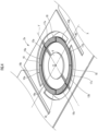
- the two-dimensional light deflector 2 when reflecting the laser light 4a by the micromirror 9, the two-dimensional light deflector 2 can emit light to the front of the two-dimensional light deflector 2 and further scan in two directions, namely, an X-axis direction and a Y-axis direction.
- the piezoelectric actuator 10a is divided by the two dividing grooves 18 into sections 16a to 16c in order from the upper side. Meanwhile, the piezoelectric actuator 10b is divided by the two dividing grooves 18 into sections 17a to 17c in order from the upper side.
- a drive voltage can be individually applied to the piezoelectric crystal film of the sections 16a to 16c and 17a to 17c.
- the micromirror 9 can be oscillated around the Y-axis by applying a predetermined voltage V1 to the sections 16a, 16c, and 17b, and applying a voltage V2, which has an opposite phase from that of V1, to the sections 16b, 17a, and 17c.
- FIG. 5 is a flowchart for manufacturing the piezoelectric element. Further, FIG. 6 illustrates the cross-sectional structure of a piezoelectric element 30 manufactured by the manufacturing method of FIG. 5 , and FIG. 7 illustrates the crystal orientation image of the PZT film 25 of the piezoelectric element 30.
- a tetragonal PZT film 25 having a film thickness of 4 to 5 ⁇ m is formed as a piezoelectric crystal film on the upper surface of the SRO film 24 at a temperature of 550°C by arc discharge reactive ion plating (ADRIP) (STEP04).
- ADRIP arc discharge reactive ion plating
- the piezoelectric element 30 is formed, in which the TiO 2 film 22 as the adhesion layer, the Pt film 23 as the lower electrode (LE) of the upper surface thereof, the SRO film 24 as the buffer layer of the upper surface of the Pt film 23, the PZT film 25 of the upper surface thereof, and the Pt film 26 as the upper electrode (UE) of the upper surface thereof are stacked on the upper surface of the Si core substrate 27 composed of the Si substrate 20 and the SiO 2 film 21, as illustrated in FIG. 6 .
- the PZT film 25 of the piezoelectric element 30 formed as described above is a polycrystalline film in which a plurality of columnar PZT crystal grains are bound in a direction perpendicular to a surface of the Pt film 23 (SRO film 24) as the lower electrode.
- the piezoelectric element 30 has a structure in which the PZT film 25 composed of a group of columnar crystal grains is placed between the surface of the Pt film 23 as the lower electrode and the surface of the Pt film 26 as the upper electrode.
- the PZT crystal that forms the PZT film 25 is a tetragonal crystal, and when a ⁇ 100> direction is defined as an a-axis, a ⁇ 010> direction is defined as a b-axis, and a ⁇ 001> direction is defined as a c-axis, the a-axis and b-axis are orthogonal, and the c-axis is orthogonal to a plane containing the a-axis and the b-axis.
- the tetragonal crystal is longer in the c-axis direction, and polarized in the c-axis direction.
- FIG. 7 is a diagram schematically illustrating two perpendicularly oriented parts 25a and 25a', and two obliquely oriented parts 25b and 25b' of the PZT crystal constituting the PZT film 25.
- Each of the perpendicularly oriented parts 25a and 25a' and the obliquely oriented parts 25b and 25b' corresponds to one unit of the crystal grains of the polycrystalline film that forms the PZT film 25.
- each of the perpendicularly oriented parts 25a and 25a', and the obliquely oriented parts 25b and 25b' may coexist in one unit of the polycrystalline body.
- the c-axis stretches (or compresses), and the surface orthogonal to the c-axis is isotropically compressed (or stretched).
- the piezoelectric actuators 6a, 6b, 10a, and 10b having the piezoelectric elements 30 formed therein to operate as described above.
- the PZT film 25 isotropically compresses (or stretches) in the film surface direction, thus making the PZT film 25 usable for piezoelectric actuators of any shapes.
- the manufacturing method of the above-described embodiment is merely an example, and the manufacturing method is not limited to the manufacturing method of the present embodiment as long as a piezoelectric film composed of uniaxially oriented columnar polycrystalline body containing perpendicularly oriented parts and obliquely oriented parts is obtained.
- the piezoelectric element of the comparative form differs from the method for manufacturing the piezoelectric element 30 of the embodiment only in that, after the TiO 2 film is formed (STEP01), the TiO 2 film is annealed and the Pt film is formed at a high temperature. The following will describe only the differences.
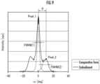
- FIG. 8 illustrates the results of measurement of the PZT film 25 obtained by the X-ray diffraction ⁇ -2 ⁇ measurement method.
- the upper electrode the Pt film 26
- the Pt film 26 shields X-rays, so that a piezoelectric element not provided with an upper electrode is used.
- a piezoelectric element may be used, in which the Pt film 26 is partially etched after the Pt film 26 is formed as the upper electrode. The crystal orientation properties of the PZT film 25 will remain unchanged even if the upper electrode is not provided.
- the horizontal axis represents a reflected X-ray angle 2 ⁇ [deg]
- the vertical axis represents a reflected X-ray intensity ([cps: counts per sec]).
- the scanning angle is 20° to 50°
- Cu-2K ⁇ 1 is used for incident X-rays.
- the PZT film of the comparative form as in the embodiment, only the peaks of the (001) surface reflection and the (002) surface reflection of the PZT film, and the (111) surface reflection of the Pt film were observed (not illustrated). This verified that the PZT film of the comparative form is also c-axis oriented through the SRO film on the (111) surface of the Pt film.
- the FWHMs of the main peak and the subpeaks were 5.0° and 8.36°, respectively.
- a position ⁇ ps of the peak of the subpeak (subpeak Ps) corresponds to the tilt angle ⁇ of the main c-axis of the obliquely oriented part 25b with respect to the main c-axis of the perpendicularly oriented part 25a. That is,
- ⁇ (10° in this case) in the present embodiment.
- the perpendicularly oriented part 25a is a group of crystals having a c-axis inclination distribution in which the FWHM is 5.0°
- the obliquely oriented part 25b is a group of crystals having a c-axis inclination distribution in which the FWHM is 8.36°.
- Both groups of crystals are discrete groups of crystals that have the c-axis orientations corresponding to the main peak Pm and the subpeak Ps as the centers of distribution.
- the c-axis of the obliquely oriented part 25b is inclined in all circumferential directions from 0° to 360° with respect to the c-axis of the perpendicularly oriented part 25a.
- the FWHM of the reflection peak was 3.1°.
- the PZT crystals of the PZT film of the comparative form are composed of only the perpendicularly oriented parts, and the perpendicularly oriented parts are a group of crystals having a c-axis inclination distribution that is narrower than that of the embodiment.
- the PZT film of the comparative form is a PZT film in which the crystal orientation of the PZT crystals exhibits high regularity.
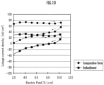
- the horizontal axis represents an electric field [V/ ⁇ m] applied to the PZT film 25 when a voltage is applied to the lower electrode (the Pt film 23) and the upper electrode (the Pt film 26) of the piezoelectric element 30, and the vertical axis represents the leakage current density [nA/cm 2 ] when a voltage is applied.
- the relationship between the electric field and the leakage current density of the piezoelectric element 30 of the embodiment is indicated by the solid line
- the relationship between the electric field and the leakage current density of the piezoelectric element of the comparative form is indicated by the dashed line.
- the voltage boost side (upper curve) is measured, and then the voltage drop side (lower curve) is measured.
- the voltage is applied in a pattern of 0[V] ⁇ measurement voltage 1 ⁇ 0[V] ⁇ measurement voltage 2 ⁇ and so on.
- the application of the voltages is performed in regions where the electric field is 2.0 [V/ ⁇ m] or more, avoiding unstable regions.
- the piezoelectric element 30 of the embodiment exhibits a leakage current of approximately 30 [nA/cm 2 ] in the first direction (positive value) when the voltage is boosted (the upper curve of the solid line). Then, when the voltage is stepped down (the lower curve of the solid line), the leakage current flowing in the first direction (positive value) decreases at an electric field of 10.0 to 8.0 [V/ ⁇ m], the leakage current becomes 0 at an electric field of 8.0 [V/ ⁇ m], and the leakage current flowing in the second direction (negative value) increases at an electric field of 8.0 to 2.0 [V/ ⁇ m]. In other words, the piezoelectric element 30 reverses the polarity of the leakage current during voltage step-down except for unstable regions. The reason why the polarity reversal of the leakage current does not immediately take place when the voltage is stepped down is considered to be due to the hysteresis of the piezoelectric crystals.
- the piezoelectric element of the comparative form exhibits a leakage current of approximately 70 [nA/cm 2 ] in the first direction (positive value) when the voltage is boosted (the upper curve of the dashed line). Then, when the voltage is stepped down (the lower curve of the dashed line), the leakage current flowing in the first direction (positive value) at an electric field of 10.0 to 2.0 [V/ ⁇ m] decreases to approximately 70 to 0 [nA/cm 2 ].
- the leakage current increases when the voltage is boosted and decreases when the voltage is stepped down.
- the leakage current reverses its flowing direction and increases.
- the leakage current increases when a voltage is boosted, and decreases when the voltage is stepped down.
- FIG. 11 is a list comparing the measurement results of the electric field resistance, which is the operating limit electric field of the piezoelectric element 30 of the embodiment and the piezoelectric element of the comparative form, and the endurance time and a piezoelectric constant d 31 in an endurance test simulating the operating conditions of the meander-type piezoelectric actuators 6a and 6b and the semi-annular piezoelectric actuators 10a and 10b used for the two-dimensional light deflector 2.
- the electric field resistance, the endurance time, and the piezoelectric constant d 31 of the piezoelectric element 30 of the embodiment are 21.8 [V/ ⁇ m], 4000 hrs. or more, and 152 [pm/V], respectively.
- the electric field resistance, the endurance time, and the piezoelectric constant d 31 of the piezoelectric element of the comparative form are 14.0 [V/ ⁇ m], 1000 hrs. or less, and 152 [pm/V], respectively. Both the electric field resistance and the endurance time have been improved over the piezoelectric element 30 of the comparative embodiment.
- the piezoelectric constant d 31 characteristics equivalent to those of the piezoelectric element of the comparative form are obtained even in the case of the piezoelectric element 30 of the embodiment provided with the obliquely oriented parts 25b.
- the piezoelectric element 30 of the present embodiment has improved electric field resistance and endurance time due to the structure described below.
- the PZT crystal that forms the PZT film 25 of the present embodiment is a columnar uniaxially oriented polycrystalline body in which the c-axis of the tetragonal crystal is oriented in the direction orthogonal to the film surface of the Pt film 23 (the SRO film 24) (the directions of the a-axis and the b-axis are arbitrary).
- the columnar uniaxially oriented polycrystalline body is provided with the perpendicularly oriented parts 25a and the obliquely oriented parts 25b.
- the obliquely oriented parts 25b are dispersed on the film surface of the PZT film 25.
- the c-axis of the perpendicularly oriented part 25a and the c-axis of the obliquely oriented part 25b are provided with the inclination distributions (each of the main peak and the subpeaks has an axis distribution).
- the film strain that occurs when the PZT crystal is deformed by applying an electric field to the PZT film 25 can be dispersed throughout the PZT film 25 so as to be mitigated.
- the leakage current resistance characteristic is improved by providing the c-axis of the obliquely oriented part 25b spaced apart (dispersedly) by an angle ⁇ from the c-axis of the perpendicularly oriented part 25a, so that the endurance time can be prolonged.
- the tilt angle ⁇ of the c-axis of the obliquely oriented part 25b is preferably set to be larger than 6° and below 19°. This is because, if the tilt angle ⁇ of the c-axis of the obliquely oriented part 25b is set to 6° or less, then the electric field resistance and the endurance time deteriorate due to assimilation to the angle distribution of the c-axis of the perpendicularly oriented part 25a.
- the tilt angle ⁇ of the c-axis of the obliquely oriented part 25b is set to 19° or more, then a ⁇ 111> axis appears, and the piezoelectric properties of the PZT film deteriorate.
- the tilt angle ⁇ is ideally set to 7° or more and 13° or less, considering the angle distribution of the c-axis of the obliquely oriented part 25b.
- the abundance ratio of the obliquely oriented part 25b of the PZT film 25 is such that the reflected X-ray intensity ratio Rp is 0.1 to 1. If Rp is below 0.1, then the effect of the obliquely oriented part 25b cannot be obtained. Further, if Rp is greater than 1, then the disturbance of the c-axis orientation of the PZT film 25 becomes excessive, causing the piezoelectric constant d 31 to lower.
- a preferable Rp is 0.15 or more at which the improvement of the electric field resistance characteristic by the obliquely oriented part 25b is saturated, or 0.45 or less at which an improved endurance life value does not decrease.
- the PZT crystals forming the PZT film 25 of the piezoelectric element 30 of the embodiment include the perpendicularly oriented parts 25a having the c-axes in the direction orthogonal to the plane of the Pt film 23 (SRO film 24) and the obliquely oriented parts 25b having the c-axes inclined (tilted) by the angle ⁇ with respect to the c-axes of the perpendicularly oriented part 25a.
- the PZT crystals allow for the high withstand voltage, the prolonged endurance time, and the piezoelectric constant of d 31 that is not compromised. This enables the piezoelectric element 30 of the present invention to provide a highly reliable two-dimensional light deflector.
- the improved withstand voltage and endurance time of the piezoelectric element 30 of the embodiment makes it possible to, for example, apply a higher voltage (electric field) to the piezoelectric element 30 to increase the range of movement of the actuators.
- the thicknesses of the thin films constituting the piezoelectric element 30 and the methods for forming the films are merely examples, and can be changed.
- the piezoelectric crystal film may be made of a material having piezoelectric properties other than PZT.
- the TiO 2 film 22 as the adhesion layer and the SRO film 24 as the buffer layer are not constituents essential to the piezoelectric element of the present invention, and may be omitted.
Landscapes
- Engineering & Computer Science (AREA)
- Chemical & Material Sciences (AREA)
- Physics & Mathematics (AREA)
- Manufacturing & Machinery (AREA)
- Ceramic Engineering (AREA)
- Organic Chemistry (AREA)
- Mechanical Engineering (AREA)
- Metallurgy (AREA)
- Materials Engineering (AREA)
- Chemical Kinetics & Catalysis (AREA)
- General Physics & Mathematics (AREA)
- Optics & Photonics (AREA)
- Computer Hardware Design (AREA)
- Microelectronics & Electronic Packaging (AREA)
- Micromachines (AREA)
- Physical Vapour Deposition (AREA)
- General Electrical Machinery Utilizing Piezoelectricity, Electrostriction Or Magnetostriction (AREA)
- Mechanical Optical Scanning Systems (AREA)
- Mechanical Light Control Or Optical Switches (AREA)
Claims (7)
- Élément piézoélectrique comprenantun substrat (27) dont au moins une surface est plane ;un premier film d'électrode (23) placé sur le plan du substrat (27) ;un film de cristal piézoélectrique tétragonal (25) placé sur le premier film d'électrode (23) ; etun deuxième film d'électrode (26) placé sur une surface du film de cristal piézoélectrique (25), la surface faisant face au premier film d'électrode (23),dans lequel le film cristallin piézoélectrique (25) est un corps polycristallin à orientation uniaxiale composé de grains de cristal colonnaires avec un axe c du cristal tétragonal orienté dans une direction perpendiculaire au premier film d'électrode (23),le corps polycristallin comprend une partie orientée perpendiculairement (25a) ayant un axe c dans une direction perpendiculaire au premier film d'électrode (23) et une partie orientée obliquement (25b, 25b') ayant un axe c incliné par rapport à l'axe c de la partie orientée perpendiculairement (25a), etl'axe c de la partie orientée perpendiculairement (25a) et l'axe c de la partie orientée obliquement (25b, 25b') ont chacun une distribution, et une distribution de l'axe c de la partie orientée obliquement (25b, 25b') est discrète par rapport à une distribution de l'axe c de la partie orientée perpendiculairement (25a) ;caractérisé en ce queun rapport d'intensité Rp dans une courbe de bascule des rayons X de la partie orientée obliquement (25b, 25b') par rapport à la partie orientée perpendiculairement (25a) est compris entre 0,1 et 1.
- L'élément piézoélectrique selon la revendication 1, dans lequel l'axe c de la partie orientée obliquement (25b, 25b') est incliné dans toutes les directions circonférentielles de 0° à 360°, l'axe c de la partie orientée perpendiculairement (25a) étant un axe de rotation.
- L'élément piézoélectrique selon l'une quelconque des revendications 1 à 2, dans lequel un angle d'inclinaison φ de l'axe c de la partie orientée obliquement (25b, 25b') par rapport à l'axe c de la partie orientée perpendiculairement (25a) du film cristallin piézoélectrique (25) est supérieur à 6° et inférieur à 19°.
- L'élément piézoélectrique selon l'une des revendications 1 à 3, dans lequel le film cristallin piézoélectrique (25) est du titanate de zirconate de plomb et le film de la première électrode (23) est du platine.
- L'élément piézoélectrique selon l'une des revendications 1 à 4, dans lequel la surface du film de la première électrode (23) est une surface (111).
- L'élément piézoélectrique selon l'une des revendications 1 à 5, dans lequel le substrat (27) est un substrat à noyau de Si en forme de plaque, dans lequel un film d'oxyde de silicium, SiO2, (21) a été formé sur une surface supérieure d'un substrat de silicium, Si, (20).
- L'élément piézoélectrique selon l'une des revendications 1 à 6, comportant en outre une couche d'adhésion (22) d'un film d'oxyde de titane amorphe, TiO2, sur le substrat (27),le film de la première électrode (23) étant placé sur le substrat (27) par l'intermédiaire de la couche d'adhésion (22),une couche tampon (24) d'un film de SrRuO3, SRO, ayant une structure de pérovskite est formée sur le premier film d'électrode (23), etle film cristallin piézoélectrique (25) est placé sur le premier film d'électrode (23) par l'intermédiaire de la couche tampon (24).
Applications Claiming Priority (2)
| Application Number | Priority Date | Filing Date | Title |
|---|---|---|---|
| JP2020183527A JP7616864B2 (ja) | 2020-11-02 | 2020-11-02 | 圧電素子及び当該圧電素子の製造方法 |
| PCT/JP2021/038453 WO2022091843A1 (fr) | 2020-11-02 | 2021-10-18 | Élément piézoélectrique et procédé de fabrication d'élément piézoélectrique |
Publications (3)
| Publication Number | Publication Date |
|---|---|
| EP4228014A1 EP4228014A1 (fr) | 2023-08-16 |
| EP4228014A4 EP4228014A4 (fr) | 2024-04-03 |
| EP4228014B1 true EP4228014B1 (fr) | 2025-03-12 |
Family
ID=81382594
Family Applications (1)
| Application Number | Title | Priority Date | Filing Date |
|---|---|---|---|
| EP21885962.7A Active EP4228014B1 (fr) | 2020-11-02 | 2021-10-18 | Élément piézoélectrique et procédé de fabrication d'élément piézoélectrique |
Country Status (5)
| Country | Link |
|---|---|
| US (1) | US20230422621A1 (fr) |
| EP (1) | EP4228014B1 (fr) |
| JP (1) | JP7616864B2 (fr) |
| CN (1) | CN116507582A (fr) |
| WO (1) | WO2022091843A1 (fr) |
Families Citing this family (2)
| Publication number | Priority date | Publication date | Assignee | Title |
|---|---|---|---|---|
| US11693233B2 (en) * | 2020-06-19 | 2023-07-04 | Microsoft Technology Licensing, Llc | Microelectromechanical system (MEMS) scanner having actuator pairs cantilevered adjacent to opposite sides of a scanning mirror |
| JP2023162833A (ja) | 2022-04-27 | 2023-11-09 | 株式会社リコー | 画像処理装置、読取装置、画像形成装置および画像処理方法 |
Family Cites Families (6)
| Publication number | Priority date | Publication date | Assignee | Title |
|---|---|---|---|---|
| JP5052835B2 (ja) | 2006-07-27 | 2012-10-17 | スタンレー電気株式会社 | 圧電アクチュエータ及びその製造方法 |
| US20110079883A1 (en) | 2009-10-01 | 2011-04-07 | Canon Kabushiki Kaisha | Ferroelectric thin film |
| JP2013197522A (ja) | 2012-03-22 | 2013-09-30 | Ricoh Co Ltd | 圧電体薄膜素子とその製造方法、該圧電体薄膜素子を用いた液滴吐出ヘッドおよびインクジェット記録装置 |
| JP6478023B2 (ja) | 2014-03-18 | 2019-03-06 | セイコーエプソン株式会社 | 圧電素子、圧電アクチュエーター装置、液体噴射ヘッド、液体噴射装置及び超音波測定装置 |
| JP6560897B2 (ja) | 2015-05-20 | 2019-08-14 | スタンレー電気株式会社 | 圧電膜の積層体とその製造方法及び光スキャナ |
| JP2017157773A (ja) | 2016-03-04 | 2017-09-07 | 株式会社リコー | 電気機械変換素子、液体吐出ヘッド、液体吐出ユニット及び液体を吐出する装置 |
-
2020
- 2020-11-02 JP JP2020183527A patent/JP7616864B2/ja active Active
-
2021
- 2021-10-18 WO PCT/JP2021/038453 patent/WO2022091843A1/fr not_active Ceased
- 2021-10-18 EP EP21885962.7A patent/EP4228014B1/fr active Active
- 2021-10-18 US US18/033,696 patent/US20230422621A1/en active Pending
- 2021-10-18 CN CN202180073710.5A patent/CN116507582A/zh active Pending
Also Published As
| Publication number | Publication date |
|---|---|
| JP2022073501A (ja) | 2022-05-17 |
| CN116507582A (zh) | 2023-07-28 |
| WO2022091843A1 (fr) | 2022-05-05 |
| EP4228014A4 (fr) | 2024-04-03 |
| EP4228014A1 (fr) | 2023-08-16 |
| JP7616864B2 (ja) | 2025-01-17 |
| US20230422621A1 (en) | 2023-12-28 |
Similar Documents
| Publication | Publication Date | Title |
|---|---|---|
| EP2827183B1 (fr) | Dispositif d'entraînement de miroir et son procédé de commande | |
| JP7237146B2 (ja) | マイクロミラーデバイスおよびマイクロミラーデバイスの駆動方法 | |
| JP5264954B2 (ja) | ミラー駆動装置及び方法 | |
| US8098415B2 (en) | Vibrating mirror element | |
| EP2827182B1 (fr) | Dispositif d'entraînement de miroir et son procédé de commande | |
| JP5224617B2 (ja) | 圧電アクチュエータ、可変容量コンデンサ及び光偏向素子 | |
| US10281716B2 (en) | Mirror driving device and driving method thereof | |
| US20130063800A1 (en) | Mirror driving apparatus, method of driving same and method of manufacturing same | |
| KR20030085538A (ko) | 압전소자, 잉크젯헤드, 각속도센서 및 이들의 제조방법,그리고 잉크젯방식 기록장치 | |
| EP3340325A1 (fr) | Élément piézo-électrique, procédé de fabrication de celui-ci et actionneur piézoélectrique | |
| JP7601961B2 (ja) | マイクロミラーデバイス | |
| US20220043256A1 (en) | Micromirror device | |
| EP4228014A1 (fr) | Élément piézoélectrique et procédé de fabrication d'élément piézoélectrique | |
| US12345876B2 (en) | Micromirror device | |
| US12438479B2 (en) | Piezoelectric actuator and optical scanning apparatus | |
| US20230309409A1 (en) | Piezoelectric element and mems mirror | |
| US20230263064A1 (en) | Piezoelectric element and mems mirror | |
| US20230263065A1 (en) | Piezoelectric element and mems mirror | |
| EP4626210A1 (fr) | Dispositif piézoélectrique à film mince | |
| WO2023042704A1 (fr) | Élément piézoélectrique, actionneur piézoélectrique, tête d'évacuation de gouttelettes de liquide, dispositif d'évacuation de gouttelettes de liquide et mémoire ferroélectrique |
Legal Events
| Date | Code | Title | Description |
|---|---|---|---|
| STAA | Information on the status of an ep patent application or granted ep patent |
Free format text: STATUS: THE INTERNATIONAL PUBLICATION HAS BEEN MADE |
|
| PUAI | Public reference made under article 153(3) epc to a published international application that has entered the european phase |
Free format text: ORIGINAL CODE: 0009012 |
|
| STAA | Information on the status of an ep patent application or granted ep patent |
Free format text: STATUS: REQUEST FOR EXAMINATION WAS MADE |
|
| 17P | Request for examination filed |
Effective date: 20230512 |
|
| AK | Designated contracting states |
Kind code of ref document: A1 Designated state(s): AL AT BE BG CH CY CZ DE DK EE ES FI FR GB GR HR HU IE IS IT LI LT LU LV MC MK MT NL NO PL PT RO RS SE SI SK SM TR |
|
| DAV | Request for validation of the european patent (deleted) | ||
| DAX | Request for extension of the european patent (deleted) | ||
| REG | Reference to a national code |
Free format text: PREVIOUS MAIN CLASS: H01L0041187000 Ipc: B81B0003000000 Ref country code: DE Ref legal event code: R079 Ref document number: 602021027648 Country of ref document: DE Free format text: PREVIOUS MAIN CLASS: H01L0041187000 Ipc: B81B0003000000 |
|
| STAA | Information on the status of an ep patent application or granted ep patent |
Free format text: STATUS: EXAMINATION IS IN PROGRESS |
|
| A4 | Supplementary search report drawn up and despatched |
Effective date: 20240229 |
|
| RIC1 | Information provided on ipc code assigned before grant |
Ipc: H10N 30/87 20230101ALI20240223BHEP Ipc: H10N 30/853 20230101ALI20240223BHEP Ipc: H10N 30/20 20230101ALI20240223BHEP Ipc: H10N 30/00 20230101ALI20240223BHEP Ipc: H10N 30/079 20230101ALI20240223BHEP Ipc: H10N 30/06 20230101ALI20240223BHEP Ipc: G02B 26/10 20060101ALI20240223BHEP Ipc: G02B 26/08 20060101ALI20240223BHEP Ipc: C23C 14/32 20060101ALI20240223BHEP Ipc: C23C 14/08 20060101ALI20240223BHEP Ipc: B81B 3/00 20060101AFI20240223BHEP |
|
| 17Q | First examination report despatched |
Effective date: 20240313 |
|
| GRAP | Despatch of communication of intention to grant a patent |
Free format text: ORIGINAL CODE: EPIDOSNIGR1 |
|
| STAA | Information on the status of an ep patent application or granted ep patent |
Free format text: STATUS: GRANT OF PATENT IS INTENDED |
|
| INTG | Intention to grant announced |
Effective date: 20241023 |
|
| RIN1 | Information on inventor provided before grant (corrected) |
Inventor name: TANAKA, HARUKI |
|
| GRAS | Grant fee paid |
Free format text: ORIGINAL CODE: EPIDOSNIGR3 |
|
| GRAA | (expected) grant |
Free format text: ORIGINAL CODE: 0009210 |
|
| STAA | Information on the status of an ep patent application or granted ep patent |
Free format text: STATUS: THE PATENT HAS BEEN GRANTED |
|
| AK | Designated contracting states |
Kind code of ref document: B1 Designated state(s): AL AT BE BG CH CY CZ DE DK EE ES FI FR GB GR HR HU IE IS IT LI LT LU LV MC MK MT NL NO PL PT RO RS SE SI SK SM TR |
|
| REG | Reference to a national code |
Ref country code: GB Ref legal event code: FG4D |
|
| REG | Reference to a national code |
Ref country code: CH Ref legal event code: EP |
|
| REG | Reference to a national code |
Ref country code: DE Ref legal event code: R096 Ref document number: 602021027648 Country of ref document: DE |
|
| REG | Reference to a national code |
Ref country code: IE Ref legal event code: FG4D |
|
| PG25 | Lapsed in a contracting state [announced via postgrant information from national office to epo] |
Ref country code: RS Free format text: LAPSE BECAUSE OF FAILURE TO SUBMIT A TRANSLATION OF THE DESCRIPTION OR TO PAY THE FEE WITHIN THE PRESCRIBED TIME-LIMIT Effective date: 20250612 |
|
| PG25 | Lapsed in a contracting state [announced via postgrant information from national office to epo] |
Ref country code: FI Free format text: LAPSE BECAUSE OF FAILURE TO SUBMIT A TRANSLATION OF THE DESCRIPTION OR TO PAY THE FEE WITHIN THE PRESCRIBED TIME-LIMIT Effective date: 20250312 |
|
| PG25 | Lapsed in a contracting state [announced via postgrant information from national office to epo] |
Ref country code: ES Free format text: LAPSE BECAUSE OF FAILURE TO SUBMIT A TRANSLATION OF THE DESCRIPTION OR TO PAY THE FEE WITHIN THE PRESCRIBED TIME-LIMIT Effective date: 20250312 |
|
| REG | Reference to a national code |
Ref country code: LT Ref legal event code: MG9D |
|
| PG25 | Lapsed in a contracting state [announced via postgrant information from national office to epo] |
Ref country code: NO Free format text: LAPSE BECAUSE OF FAILURE TO SUBMIT A TRANSLATION OF THE DESCRIPTION OR TO PAY THE FEE WITHIN THE PRESCRIBED TIME-LIMIT Effective date: 20250612 |
|
| PG25 | Lapsed in a contracting state [announced via postgrant information from national office to epo] |
Ref country code: HR Free format text: LAPSE BECAUSE OF FAILURE TO SUBMIT A TRANSLATION OF THE DESCRIPTION OR TO PAY THE FEE WITHIN THE PRESCRIBED TIME-LIMIT Effective date: 20250312 |
|
| REG | Reference to a national code |
Ref country code: NL Ref legal event code: MP Effective date: 20250312 |
|
| PG25 | Lapsed in a contracting state [announced via postgrant information from national office to epo] |
Ref country code: LV Free format text: LAPSE BECAUSE OF FAILURE TO SUBMIT A TRANSLATION OF THE DESCRIPTION OR TO PAY THE FEE WITHIN THE PRESCRIBED TIME-LIMIT Effective date: 20250312 |
|
| PG25 | Lapsed in a contracting state [announced via postgrant information from national office to epo] |
Ref country code: BG Free format text: LAPSE BECAUSE OF FAILURE TO SUBMIT A TRANSLATION OF THE DESCRIPTION OR TO PAY THE FEE WITHIN THE PRESCRIBED TIME-LIMIT Effective date: 20250312 Ref country code: GR Free format text: LAPSE BECAUSE OF FAILURE TO SUBMIT A TRANSLATION OF THE DESCRIPTION OR TO PAY THE FEE WITHIN THE PRESCRIBED TIME-LIMIT Effective date: 20250613 |
|
| REG | Reference to a national code |
Ref country code: AT Ref legal event code: MK05 Ref document number: 1774916 Country of ref document: AT Kind code of ref document: T Effective date: 20250312 |
|
| PG25 | Lapsed in a contracting state [announced via postgrant information from national office to epo] |
Ref country code: NL Free format text: LAPSE BECAUSE OF FAILURE TO SUBMIT A TRANSLATION OF THE DESCRIPTION OR TO PAY THE FEE WITHIN THE PRESCRIBED TIME-LIMIT Effective date: 20250312 |
|
| PG25 | Lapsed in a contracting state [announced via postgrant information from national office to epo] |
Ref country code: SE Free format text: LAPSE BECAUSE OF FAILURE TO SUBMIT A TRANSLATION OF THE DESCRIPTION OR TO PAY THE FEE WITHIN THE PRESCRIBED TIME-LIMIT Effective date: 20250312 |
|
| PG25 | Lapsed in a contracting state [announced via postgrant information from national office to epo] |
Ref country code: SM Free format text: LAPSE BECAUSE OF FAILURE TO SUBMIT A TRANSLATION OF THE DESCRIPTION OR TO PAY THE FEE WITHIN THE PRESCRIBED TIME-LIMIT Effective date: 20250312 |
|
| PG25 | Lapsed in a contracting state [announced via postgrant information from national office to epo] |
Ref country code: PT Free format text: LAPSE BECAUSE OF FAILURE TO SUBMIT A TRANSLATION OF THE DESCRIPTION OR TO PAY THE FEE WITHIN THE PRESCRIBED TIME-LIMIT Effective date: 20250714 |
|
| PG25 | Lapsed in a contracting state [announced via postgrant information from national office to epo] |
Ref country code: IT Free format text: LAPSE BECAUSE OF FAILURE TO SUBMIT A TRANSLATION OF THE DESCRIPTION OR TO PAY THE FEE WITHIN THE PRESCRIBED TIME-LIMIT Effective date: 20250312 Ref country code: PL Free format text: LAPSE BECAUSE OF FAILURE TO SUBMIT A TRANSLATION OF THE DESCRIPTION OR TO PAY THE FEE WITHIN THE PRESCRIBED TIME-LIMIT Effective date: 20250312 |
|
| PG25 | Lapsed in a contracting state [announced via postgrant information from national office to epo] |
Ref country code: AT Free format text: LAPSE BECAUSE OF FAILURE TO SUBMIT A TRANSLATION OF THE DESCRIPTION OR TO PAY THE FEE WITHIN THE PRESCRIBED TIME-LIMIT Effective date: 20250312 |
|
| PG25 | Lapsed in a contracting state [announced via postgrant information from national office to epo] |
Ref country code: CZ Free format text: LAPSE BECAUSE OF FAILURE TO SUBMIT A TRANSLATION OF THE DESCRIPTION OR TO PAY THE FEE WITHIN THE PRESCRIBED TIME-LIMIT Effective date: 20250312 Ref country code: EE Free format text: LAPSE BECAUSE OF FAILURE TO SUBMIT A TRANSLATION OF THE DESCRIPTION OR TO PAY THE FEE WITHIN THE PRESCRIBED TIME-LIMIT Effective date: 20250312 |
|
| PG25 | Lapsed in a contracting state [announced via postgrant information from national office to epo] |
Ref country code: RO Free format text: LAPSE BECAUSE OF FAILURE TO SUBMIT A TRANSLATION OF THE DESCRIPTION OR TO PAY THE FEE WITHIN THE PRESCRIBED TIME-LIMIT Effective date: 20250312 |
|
| PG25 | Lapsed in a contracting state [announced via postgrant information from national office to epo] |
Ref country code: SK Free format text: LAPSE BECAUSE OF FAILURE TO SUBMIT A TRANSLATION OF THE DESCRIPTION OR TO PAY THE FEE WITHIN THE PRESCRIBED TIME-LIMIT Effective date: 20250312 |
|
| PG25 | Lapsed in a contracting state [announced via postgrant information from national office to epo] |
Ref country code: IS Free format text: LAPSE BECAUSE OF FAILURE TO SUBMIT A TRANSLATION OF THE DESCRIPTION OR TO PAY THE FEE WITHIN THE PRESCRIBED TIME-LIMIT Effective date: 20250712 |
|
| REG | Reference to a national code |
Ref country code: DE Ref legal event code: R097 Ref document number: 602021027648 Country of ref document: DE |
|
| PGFP | Annual fee paid to national office [announced via postgrant information from national office to epo] |
Ref country code: DE Payment date: 20251008 Year of fee payment: 5 |
|
| PG25 | Lapsed in a contracting state [announced via postgrant information from national office to epo] |
Ref country code: DK Free format text: LAPSE BECAUSE OF FAILURE TO SUBMIT A TRANSLATION OF THE DESCRIPTION OR TO PAY THE FEE WITHIN THE PRESCRIBED TIME-LIMIT Effective date: 20250312 |
|
| PLBE | No opposition filed within time limit |
Free format text: ORIGINAL CODE: 0009261 |
|
| STAA | Information on the status of an ep patent application or granted ep patent |
Free format text: STATUS: NO OPPOSITION FILED WITHIN TIME LIMIT |
|
| REG | Reference to a national code |
Ref country code: CH Ref legal event code: L10 Free format text: ST27 STATUS EVENT CODE: U-0-0-L10-L00 (AS PROVIDED BY THE NATIONAL OFFICE) Effective date: 20260121 |
|
| 26N | No opposition filed |
Effective date: 20251215 |