EP4235190A1 - Dispositif micromécanique de mesure d'accélération améliorée - Google Patents
Dispositif micromécanique de mesure d'accélération améliorée Download PDFInfo
- Publication number
- EP4235190A1 EP4235190A1 EP23157012.8A EP23157012A EP4235190A1 EP 4235190 A1 EP4235190 A1 EP 4235190A1 EP 23157012 A EP23157012 A EP 23157012A EP 4235190 A1 EP4235190 A1 EP 4235190A1
- Authority
- EP
- European Patent Office
- Prior art keywords
- control
- value
- measurement
- signal
- micromechanical device
- Prior art date
- Legal status (The legal status is an assumption and is not a legal conclusion. Google has not performed a legal analysis and makes no representation as to the accuracy of the status listed.)
- Pending
Links
Images



Classifications
-
- G—PHYSICS
- G01—MEASURING; TESTING
- G01P—MEASURING LINEAR OR ANGULAR SPEED, ACCELERATION, DECELERATION, OR SHOCK; INDICATING PRESENCE, ABSENCE, OR DIRECTION, OF MOVEMENT
- G01P15/00—Measuring acceleration; Measuring deceleration; Measuring shock, i.e. sudden change of acceleration
- G01P15/02—Measuring acceleration; Measuring deceleration; Measuring shock, i.e. sudden change of acceleration by making use of inertia forces using solid seismic masses
- G01P15/08—Measuring acceleration; Measuring deceleration; Measuring shock, i.e. sudden change of acceleration by making use of inertia forces using solid seismic masses with conversion into electric or magnetic values
- G01P15/125—Measuring acceleration; Measuring deceleration; Measuring shock, i.e. sudden change of acceleration by making use of inertia forces using solid seismic masses with conversion into electric or magnetic values by capacitive pick-up
-
- B—PERFORMING OPERATIONS; TRANSPORTING
- B81—MICROSTRUCTURAL TECHNOLOGY
- B81B—MICROSTRUCTURAL DEVICES OR SYSTEMS, e.g. MICROMECHANICAL DEVICES
- B81B7/00—Microstructural systems ; Auxiliary parts of microstructural devices or systems
- B81B7/02—Microstructural systems ; Auxiliary parts of microstructural devices or systems containing distinct electrical or optical devices of particular relevance for their function, e.g. microelectro-mechanical systems [MEMS]
-
- G—PHYSICS
- G01—MEASURING; TESTING
- G01P—MEASURING LINEAR OR ANGULAR SPEED, ACCELERATION, DECELERATION, OR SHOCK; INDICATING PRESENCE, ABSENCE, OR DIRECTION, OF MOVEMENT
- G01P15/00—Measuring acceleration; Measuring deceleration; Measuring shock, i.e. sudden change of acceleration
- G01P15/02—Measuring acceleration; Measuring deceleration; Measuring shock, i.e. sudden change of acceleration by making use of inertia forces using solid seismic masses
- G01P15/08—Measuring acceleration; Measuring deceleration; Measuring shock, i.e. sudden change of acceleration by making use of inertia forces using solid seismic masses with conversion into electric or magnetic values
-
- G—PHYSICS
- G01—MEASURING; TESTING
- G01P—MEASURING LINEAR OR ANGULAR SPEED, ACCELERATION, DECELERATION, OR SHOCK; INDICATING PRESENCE, ABSENCE, OR DIRECTION, OF MOVEMENT
- G01P15/00—Measuring acceleration; Measuring deceleration; Measuring shock, i.e. sudden change of acceleration
- G01P15/02—Measuring acceleration; Measuring deceleration; Measuring shock, i.e. sudden change of acceleration by making use of inertia forces using solid seismic masses
- G01P15/08—Measuring acceleration; Measuring deceleration; Measuring shock, i.e. sudden change of acceleration by making use of inertia forces using solid seismic masses with conversion into electric or magnetic values
- G01P15/0802—Details
-
- G—PHYSICS
- G01—MEASURING; TESTING
- G01P—MEASURING LINEAR OR ANGULAR SPEED, ACCELERATION, DECELERATION, OR SHOCK; INDICATING PRESENCE, ABSENCE, OR DIRECTION, OF MOVEMENT
- G01P15/00—Measuring acceleration; Measuring deceleration; Measuring shock, i.e. sudden change of acceleration
- G01P15/02—Measuring acceleration; Measuring deceleration; Measuring shock, i.e. sudden change of acceleration by making use of inertia forces using solid seismic masses
- G01P15/08—Measuring acceleration; Measuring deceleration; Measuring shock, i.e. sudden change of acceleration by making use of inertia forces using solid seismic masses with conversion into electric or magnetic values
- G01P15/13—Measuring acceleration; Measuring deceleration; Measuring shock, i.e. sudden change of acceleration by making use of inertia forces using solid seismic masses with conversion into electric or magnetic values by measuring the force required to restore a proofmass subjected to inertial forces to a null position
- G01P15/131—Measuring acceleration; Measuring deceleration; Measuring shock, i.e. sudden change of acceleration by making use of inertia forces using solid seismic masses with conversion into electric or magnetic values by measuring the force required to restore a proofmass subjected to inertial forces to a null position with electrostatic counterbalancing means
-
- B—PERFORMING OPERATIONS; TRANSPORTING
- B81—MICROSTRUCTURAL TECHNOLOGY
- B81B—MICROSTRUCTURAL DEVICES OR SYSTEMS, e.g. MICROMECHANICAL DEVICES
- B81B2201/00—Specific applications of microelectromechanical systems
- B81B2201/02—Sensors
- B81B2201/0228—Inertial sensors
- B81B2201/0235—Accelerometers
-
- G—PHYSICS
- G01—MEASURING; TESTING
- G01P—MEASURING LINEAR OR ANGULAR SPEED, ACCELERATION, DECELERATION, OR SHOCK; INDICATING PRESENCE, ABSENCE, OR DIRECTION, OF MOVEMENT
- G01P15/00—Measuring acceleration; Measuring deceleration; Measuring shock, i.e. sudden change of acceleration
- G01P15/02—Measuring acceleration; Measuring deceleration; Measuring shock, i.e. sudden change of acceleration by making use of inertia forces using solid seismic masses
- G01P15/08—Measuring acceleration; Measuring deceleration; Measuring shock, i.e. sudden change of acceleration by making use of inertia forces using solid seismic masses with conversion into electric or magnetic values
- G01P2015/0805—Measuring acceleration; Measuring deceleration; Measuring shock, i.e. sudden change of acceleration by making use of inertia forces using solid seismic masses with conversion into electric or magnetic values being provided with a particular type of spring-mass-system for defining the displacement of a seismic mass due to an external acceleration
- G01P2015/0808—Measuring acceleration; Measuring deceleration; Measuring shock, i.e. sudden change of acceleration by making use of inertia forces using solid seismic masses with conversion into electric or magnetic values being provided with a particular type of spring-mass-system for defining the displacement of a seismic mass due to an external acceleration for defining in-plane movement of the mass, i.e. movement of the mass in the plane of the substrate
- G01P2015/0811—Measuring acceleration; Measuring deceleration; Measuring shock, i.e. sudden change of acceleration by making use of inertia forces using solid seismic masses with conversion into electric or magnetic values being provided with a particular type of spring-mass-system for defining the displacement of a seismic mass due to an external acceleration for defining in-plane movement of the mass, i.e. movement of the mass in the plane of the substrate for one single degree of freedom of movement of the mass
- G01P2015/0814—Measuring acceleration; Measuring deceleration; Measuring shock, i.e. sudden change of acceleration by making use of inertia forces using solid seismic masses with conversion into electric or magnetic values being provided with a particular type of spring-mass-system for defining the displacement of a seismic mass due to an external acceleration for defining in-plane movement of the mass, i.e. movement of the mass in the plane of the substrate for one single degree of freedom of movement of the mass for translational movement of the mass, e.g. shuttle type
Definitions
- the present invention relates to a micromechanical device for enhanced acceleration measurement.
- a micromechanical device MEMS-type sensor
- the micromechanical device comprises a capacitively controllable control structure to vary a total elastic constant of the micromechanical device (indicative of its stiffness), so as to be able to perform a first acceleration measurement with maximum full scale range and minimum sensitivity and subsequently, as a function of the result of the first acceleration measurement, perform a second acceleration measurement, optimized, with a lower full scale range and greater sensitivity.
- low-G sensors such as accelerometers and gyroscopes
- high-G sensors for sensing high accelerations (for example, having full scale ranges equal to 128 G)
- the former are used to sense usual movements (such as rotations of the cell phone screen, or movement of the wrist whereto the smartwatch is connected) of operators provided with the electronic device integrating the sensors, while the latter allow high-intensity accelerations (and therefore, abnormal events such as falls or shocks) to be sensed.
- the FSR and the measurement sensitivity are inversely proportional to each other.
- high-G sensors sense greater FSR with lower sensitivity and low-G sensors sense lower FSR with greater sensitivity.
- the sensor may comprise: two seismic masses coupled, through respective elastic elements, to a substrate and configured to abut against each other for accelerations greater than a threshold acceleration, consequently modifying the overall elastic constant of the sensor; a seismic mass coupled to a substrate through a first elastic element and configured to abut against a second elastic element for accelerations greater than a threshold acceleration; or a seismic mass coupled to a substrate through an elastic element which, for accelerations lower than a threshold acceleration, deforms completely with a first elastic constant and, for accelerations greater than the threshold acceleration, deforms only partially with a second elastic constant greater than the first elastic constant (due to a mechanical contact of the elastic element with the seismic mass which modifies the effective length of the elastic element).
- These solutions therefore base the adaptation of the elastic constant on mechanical contacts between parts of the same sensor.
- Document US 2011/132089 A1 relates to an inertial sensor formed by a semiconductor microfabrication technique (microelectro-mechanical system (MEMS) process) and for measuring inertial force such as an applied acceleration by detecting electrostatic capacitance change, and, more particularly, relates to a technique capable of selecting a plurality of measurement ranges.
- MEMS microelectro-mechanical system
- the aim of the present invention is to provide a micromechanical device, a measurement device comprising the micromechanical device, a control method of the micromechanical device and a relative computer program product that overcome the drawbacks of the prior art.
- a micromechanical device a measurement device comprising the micromechanical device, a control method of the micromechanical device and a relative computer program product are provided, as defined in the annexed claims.
- Figures are shown with reference to a triaxial Cartesian system defined by a first axis X, a second axis Y and a third axis Z, orthogonal to each other.
- Figure 1 shows a micromechanical device 50 configured to sense accelerations (hereinafter also referred to as sensor 50), according to an embodiment.
- Figure 1 is a plan view (i.e. on an XY plane defined by the X and Y axes) of the sensor 50.
- Figure 1 illustrates only the elements useful for understanding the present embodiment, and no elements or components are shown that, although present in the finished sensor, are not relevant for the present invention.
- the sensor 50 is exemplarily described herein as a uniaxial-type accelerometer (in detail, configured to sense accelerations along the X axis). However, it is apparent that the present description applies, in a similar manner, also to the case of biaxial or triaxial accelerometers.
- the sensor 50 made using MEMS technology (i.e. by semiconductor manufacturing methods), comprises a semiconductor body 51 of semiconductor material such as silicon (Si), having a surface 51a extending parallel to the XY plane (i.e., the Z axis is orthogonal to the surface 51a).
- the sensor 50 further comprises a movable structure (or seismic mass) 53 having a mass M.
- the seismic mass 53 is, for example, of semiconductor material (such as silicon or polysilicon) and extends parallel to the surface 51a of the semiconductor body 51, at a different height, along the Z axis, with respect to that of the surface 51a.
- semiconductor material such as silicon or polysilicon
- the seismic mass 53 is physically coupled to the semiconductor body 51 through a spring assembly 57 (in detail, a first spring, or first elastic element, 57a of the spring assembly 57 and a second spring, or second elastic element 57b of the spring assembly 57).
- the spring assembly 57 is, for example, of semiconductor material (such as silicon or polysilicon) and deforms (i.e. it elongates/shortens) exemplarily along the X axis.
- the spring assembly 57 has a deformation direction 60, wherealong the deformation occurs, which is parallel to the X axis and coincides with an oscillation direction 61 of the seismic mass 53 wherealong the latter oscillates in use.
- the first and the second springs 57a, 57b are serpentine springs.
- these serpentine springs are of planar type and made using MEMS technology (i.e. by semiconductor manufacturing methods). More in detail, such serpentine springs may include first portions, extending parallel to each other and to the Y axis, and second portions, extending parallel to each other and to the X axis.
- each first portion is connected, at its ends (opposite to each other along the Y axis), to respective second portions; and each second portion is connected, at its ends (opposite to each other along the X axis), to respective first portions, except for two second portions (each arranged at a respective end of this path along the X axis and joined to a single respective first portion).
- Each spring 57a, 57b of the spring assembly 57 has a respective first end 57a', 57b' and a respective second end 57a", 57b", opposite to each other along the X axis.
- the distance, measured along the X axis between the first end 57a' and the second end 57a" of the first spring 57a of the spring assembly 57 is identified with the reference L a ;
- the distance, measured along the X axis between the first end 57b' and the second end 57b" of the second spring 57b of the spring assembly 57 is identified with the reference L b .
- the springs 57a, 57b of the spring assembly 57 have a respective elastic constant (hereinafter referred to as partial elastic constant) K p having value exemplarily equal to each other.
- partial elastic constant hereinafter referred to as partial elastic constant
- two springs 57a, 57b are exemplarily present, so that the elastic constant (hereinafter referred to as equivalent elastic constant) K eq of the spring assembly 57 has a value exemplarily equal to 2K p .
- the equivalent elastic constant K eq of the spring assembly 57 has a value exemplarily equal to N ⁇ K p .
- the partial elastic constants K p and the equivalent elastic constant K eq depend on the mechanical properties and on the number of springs of the spring assembly 57 and not on the mode wherein the sensor 50 is operated.
- Each spring 57a, 57b of the spring assembly 57 is coupled, through the respective first end 57a', 57b', to a respective fixing element 64 coupled to the surface 51a of the semiconductor body 51 (in particular, each fixing element 64 is integral with the surface of the semiconductor body 51).
- Each spring 57a, 57b of the spring assembly 57 is also coupled, through the respective second end 57a", 57b", to the seismic mass 53.
- the seismic mass 53 has a first and a second lateral surface 53a, 53b opposite to each other along the X axis, and each second end 57a", 57b" is integral with a respective one of the first and the second lateral surfaces 53a, 53b. Consequently, the first seismic mass 53 is interposed, along the X axis, between the first and the second springs 57a, 57b of the spring assembly 57.
- the seismic mass 53 includes one or more first measurement electrodes 68a (movable measurement electrodes), such as protrusions (for example having a substantially rectangular shape on the XY plane) which, in use, move integral with the seismic mass 53.
- Figure 1 exemplarily shows the case wherein a first measurement electrode 68a is present, although the number of the first measurement electrodes 68a may be greater in further embodiments of the sensor 50.
- One or more second measurement electrodes 68b are integral with the semiconductor body 51, in particular with the surface 51a.
- Each of the second measurement electrodes 68b is further divided into a first portion 68b' and a second portion 68b", physically and electrically separated from each other (in detail, connected to respective pads and biasable as better described hereinafter); the first measurement electrode 68a extends between the first portion 68b' and the second portion 68b".
- each of the first measurement electrodes 68a faces, and is interposed between, the first portion 68b' of a respective second measurement electrode 68b and the second portion 68b" of this respective second measurement electrode 68b.
- Figure 1 exemplarily shows the case wherein a second measurement electrode 68b is present, although the number of the second measurement electrodes 68b may be greater in further embodiments of the sensor 50.
- the first and the second measurement electrodes 68a, 68b form a measurement structure 68 (optional) of the sensor 50 for, in use, capacitively sensing displacements along the first axis X of the seismic mass 53; these displacements are indicative of external forces acting on the sensor 50 (e.g., due to accelerations applied to the sensor 50, i.e. whereto the sensor 50 is subject).
- the distance (along the X axis) between the first measurement electrode 68a and the first portion 68b' is indicated with the reference d m1
- the distance between the first measurement electrode 68a and the second portion 68b" is indicated with the reference d m2 .
- the seismic mass 53 includes an accommodation through opening (alternatively, a cavity) 76 whereinto the measurement electrodes 68a and 68b extend.
- the seismic mass 53 encloses and delimits the accommodation through opening 76 which traverses the seismic mass 53 transversely to the surface 51a of the semiconductor body 51.
- the portions 68b' and 68b" of the second measurement electrode 68b extend into the accommodation through opening 76 and the first measurement electrode 68a protrudes into the accommodation through opening 76 and extends between the portions 68b' and 68b" of the second measurement electrode 68b.
- the seismic mass 53 includes one or more first control electrodes 72a (movable control electrodes), such as protrusions (for example having a substantially rectangular shape on the XY plane) which, in use, move integral with the seismic mass 53.
- Figure 1 exemplarily shows the case wherein a first control electrode 72a is present, although the number of the first control electrodes 72a may be greater in further embodiments of the sensor 50.
- One or more second control electrodes 72b are integral with the semiconductor body 51, in particular with the surface 51a.
- Each of the second control electrodes 72b is further divided into a first portion 72b' and a second portion 72b", separate from each other; the first control electrode 72a extends between the first portion 72b' of a respective second control electrode 72b and the second portion 72b" of the respective second control electrode 72b.
- each of the first control electrodes 72a faces, and is interposed between, the first portion 72b' of a respective second control electrode 72b and the second portion 72b" of this respective second control electrode 72b.
- Figure 1 exemplarily shows the case wherein a second measurement electrode 72b is present, although the number of the second control electrodes 72b may be greater in further embodiments of the sensor 50.
- the first and the second control electrodes 72a, 72b form a control structure 72 of the sensor 50 for, in use, capacitively controlling the operation of the sensor 50, as better discussed hereinafter.
- surfaces of the first control electrode 72a and of the first portion 72b' of the second control electrode 72b which are directly facing each other form a first control capacitor 72'; similarly, surfaces of the first control electrode 72a and of the second portion 72b" of the second control electrode 72b, directly facing each other, form a second control capacitor 72".
- the distance (along the X axis) between the first control electrode 72a and the first portion 72b' of the second control electrode 72b is indicated with the reference d c1
- the distance between the first control electrode 72a and the second portion 72b" of the second control electrode 72b is indicated with the reference d c2 .
- the seismic mass 53 has a third and a fourth lateral surface 53c and 53d which are opposite to each other along the Y axis and which join to each other the first and the second lateral surfaces 53a and 53b, and the control electrodes 72a and 72b face one of the third and the fourth lateral surfaces 53c and 53d (here the third lateral surface 53c is exemplarily considered).
- the portions 72b' and 72b" of the second control electrode 72b face the third lateral surface 53c and the first control electrode 72a protrudes, from the third lateral surface 53c, so as to extend between the portions 72b' and 72b" of the second control electrode 72b.
- first and second blocking elements 70', 70" are integral with the semiconductor body 51 (in particular, with the surface 51a of the semiconductor body 51).
- Figure 1 exemplarily illustrates two blocking elements 70' which are distant from the first lateral surface 53a of the seismic mass 53 by a distance L 1block along the first axis X;
- Figure 1 also illustrates two blocking elements 70" which are distant from the second lateral surface 53b of the seismic mass 53 by a distance L 2block along the first axis X.
- the distance d m1 is designed with a value such that d m1 >L 1block and d c1 >L 1block
- the distance d m2 is designed with a value such that d m2 >L 2block and d c2 >L 2block .
- the sensor 50 in a rest condition of the sensor 50 wherein the seismic mass 53 is not subject to accelerations along the oscillation direction 61, the sensor 50 has axial symmetry with respect to a centerline 74 orthogonal to the oscillation direction 61 and parallel to the surface 51a (in particular, parallel to the Y axis) and passing through a center (e.g., barycenter, not shown) of the seismic mass 53.
- the measurement structure 68 capacitively senses the displacements of the seismic mass 53 along the oscillation direction 61.
- the seismic mass 53 (also called rotor; and therefore the first measurement electrode 68a which is a part thereof) is biased in a per se known manner with a bias signal (in particular a first bias voltage V1, for example being square wave-shaped).
- the first bias voltage V1 oscillates, around an effective value of the bias voltage, at a bias frequency (or rotor frequency) f rot greater than a mechanical resonance frequency f res of the sensor 50.
- the bias frequency f rot is at least one order of magnitude greater than the mechanical resonance frequency f res (e.g., f rot ⁇ 10-300 kHz and f res ⁇ 1-10 kHz), so that the mechanical properties of the seismic mass 53 (e.g., its motion) are not affected by the first bias voltage V1.
- the first bias voltage V1 is provided from the outside (e.g., by a bias apparatus of a known type) to sensor pads 50, not shown and present on the surface 51a of the semiconductor body 51, and is carried by these pads to the seismic mass 53 through one or more conductive paths defined for example by conductive tracks electrically connected to the seismic mass through the blocking elements 64 and the springs 57a and 57b.
- the portions 68b' and 68b" of the second measurement electrode 68b are biased to respective second bias voltages V2' and V2", in particular of direct type (DC).
- V2' ⁇ V2" in detail, providing the respective pads electrically connected to the portions 68b' and 68b" with the respective second bias voltages V2' and V2" different from each other).
- the senor 50 is subject to an acceleration along the oscillation direction 61 (oscillation condition of the sensor 50, alternative to the rest condition), which generates an external force acting on the seismic mass 53 and causes it to oscillate along the oscillation direction 61 with respect to a rest position thereof; consequently, the springs 57a and 57b contract and elongate alternately to each other (i.e. L a ⁇ L b ) due to the contraction and elongation forces exerted thereon by the seismic mass 53.
- the distances d m1 , d m2 vary as a function of the external force applied to the sensor 50: it is therefore possible to correlate in a known manner the respective capacitance variations of the measurement capacitors 68', 68" (acquired owing to the previously described biasing of the seismic mass 53) to this external force applied.
- a difference between the respective capacitance variations of the measurement capacitors 68', 68" is zero in the rest condition of the sensor 50 (unless a possible measurement noise occurs that is not considered here as it is not relevant for the purposes of this description) and is different from zero in the oscillation condition of the sensor 50.
- the capacitance measurements may be carried out through techniques known per se, for example through transimpedance amplifiers.
- the control structure 72 capacitively controls the displacements of the seismic mass 53 along the oscillation direction 61, as better described hereinafter.
- the capacitive control occurs because of the known spring softening effect: by applying a control voltage V c variable over time (i.e. a voltage difference between the first and the second control electrodes 72a and 72b, variable over time) to the control structure 72, a respective variation over time of a total elastic constant K t of the sensor 50 occurs.
- the total elastic constant K t is indicative of the stiffness of the sensor 50 (in detail, of the oscillating assembly comprising the seismic mass 53, the spring assembly 57, the control structure 72 and, optionally, the measurement structure 68) and is a function both of the mechanical properties of the sensor 50 (e.g., stiffness and number of springs of the spring assembly 57) and of the electrical bias state of the sensor 50 (e.g., of the electrical state of the measurement structure 68 and of the control structure 72).
- the total elastic constant K t is equal to the equivalent elastic constant K eq of the spring assembly 57 (constant over time and indicative of the structure and mechanical properties of the spring assembly 57) minus a first variation ⁇ K contr of the total elastic constant (variable over time and relating to the softening provided by electrically biasing the control structure 72) and a second variation ⁇ K mis of total elastic constant (constant over time and relating to the softening provided by electrically biasing the measurement structure 68).
- the second variation ⁇ K mis of total elastic constant is considered here as constant over time since f rot >>f res and therefore the oscillation over time of the first bias voltage V1 around its effective value does not generate any perceptible time-variable effect at the work frequencies of the sensor 50 (generally lower than the resonance frequency f res ).
- V3 total control voltage, not shown and generated in a known manner
- the control voltage difference V c varies between a first value V c1 (in detail, zero) and a second value V c2 (greater than, or equal to, the first value V c1 , and variable and determined as better described hereinafter) with a frequency equal to a control frequency f c .
- the control frequency f c is generally lower than the resonance frequency f res by about an order of magnitude and therefore is exemplarily in the order of a hundred Hz, for example it is equal to about 100-200Hz.
- the control structure 72 contributes to the softening effect) and the total elastic constant K t assumes a second value K t2 lower than the first value K t1 and equal to K eq - ⁇ K contr - ⁇ K mis (with ⁇ K mis ⁇ 0 N/m).
- the attraction force is generated between the second control electrodes 72b (fixed to the semiconductor body 51 and operating as stators) and the first control electrode 72a (fixed to the seismic mass 53 and operating as a rotor configured to oscillate along the oscillation direction 61 with respect to the semiconductor body 51) and acts parallel to the oscillation direction 61 causing the reduction of the total elastic constant K t of the sensor 50.
- V c is the control voltage difference
- f res is the resonance frequency of the sensor 50 also depending on the control voltage difference V c
- ⁇ 0 is a reference resonance pulse of the sensor 50 in the absence of the control voltage difference V c (i.e.
- ⁇ is the absolute electrical permittivity of the insulator present in the control capacitors 72' and 72" (here air or vacuum)
- A is the area of the surfaces of the control electrodes 72a and 72b which face each other to form the control capacitors 72' and 72"
- M is the mass of the seismic mass 53
- FSR is the full scale range of the sensor 50 and sens is the sensitivity of the sensor 50.
- the resonance frequency f res decreases, with respect to a reference value thereof corresponding to the reference resonance pulse ⁇ 0 , when a non-zero value of the control voltage difference V c is applied between the control electrodes 72a and 72b.
- the reduction in the resonance frequency f res causes a respective reduction in the FSR and a respective increase in sensitivity.
- a mis is the area of the surfaces of the measurement electrodes 68a and 68b which face each other to form the measurement capacitors 68' and 68
- d mis is the distance between the surfaces of the measurement electrodes 68a and 68b which face each other to form the measurement capacitors 68' and 68
- a contr here is the area of the surfaces of the control electrodes 72a and 72b which face each other to form the control capacitors 72' and 72
- d contr is the distance between the surfaces of the control electrodes 72a and 72b which face each other to form the control capacitors 72' and 72".
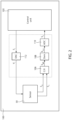
- the sensor 50 is comprised in a measurement device 100 configured to measure accelerations acting along the oscillation direction 61 (i.e. parallel to the X axis).
- the measurement device 100 implements a control method (better discussed hereinafter with reference to Figure 4 and indicated with the reference 150) which allows the sensor 50 to be controlled in order to measure these accelerations in an optimized manner.
- the measurement device 100 comprises a control unit 102 electrically coupled to the sensor 50 to control the latter and to sense the accelerations along the oscillation direction 61 whereto it is subject.
- the control unit 102 receives a measurement signal S m indicative of the acceleration sensed by the sensor 50 and generates a control signal S c for controlling the sensor 50.
- the measurement device 100 also comprises an interface unit 104 electrically coupled to the sensor 50 and to the control unit 102 to interface them with each other.
- the interface unit 104 comprises a C/V (capacitance to voltage) conversion block 106, a demodulation block 108, an analog to digital conversion, ADC, block 110 and a digital to analog conversion, DAC, block 112.
- the C/V conversion block 106 (e.g., provided through a transimpedance amplifier) is electrically coupled to the measurement structure 68 and in use receives a first sensing signal S r1 and a second sensing signal S r2 from the measurement structure 68 of the sensor 50.
- the first and the second sensing signals S r1 , S r2 are electrical signals (e.g., current signals) indicative of the capacitances of the first and, respectively, the second measurement capacitors 68', 68".
- the C/V conversion block 106 generates, on the basis of the difference between the first sensing signal S r1 and the second sensing signal S r2 , a differential signal (or differential voltage) S diff (e.g., a voltage signal) indicative of the acceleration sensed by the sensor 50.
- a differential signal or differential voltage S diff (e.g., a voltage signal) indicative of the acceleration sensed by the sensor 50.
- the demodulation block 108 receives the differential signal S diff from the C/V conversion block 106 and generates a demodulated signal (or demodulated voltage) S dem through demodulation of the differential signal S diff , in a per se known manner.
- the first component S o1 is due to the control of the control structure 72 through the control signal S c (the corresponding digital signal of the control voltage difference V c , therefore also at the control frequency f c ), while the second component S o2 is due to the biasing of the seismic mass 53 through the first bias voltage V1 at the bias frequency f rot .
- S diff S o1 +S o2 . Consequently, the demodulation block 108 removes the second component S o2 at the bias frequency f rot from the differential signal S diff to generate the demodulated signal S dem at the control frequency f c , indicative only of the sensed acceleration and not of the driving modulation (rotor signal modulation) of the sensor 50.
- the ADC block 110 receives the demodulated signal S dem and converts it from an analog signal to a digital signal in a per se known manner, thus generating at output the measurement signal S m which is received by the control unit 102.
- the control unit 102 receives at input the measurement signal S m indicative of the measured acceleration and generates at output, as better described hereinafter, the control signal S c configured to control the operation of the sensor 50.
- the control signal S c is the corresponding digital signal of the control voltage difference Vc of analog type.
- the DAC block 112 receives the control signal S c and converts it from a digital signal to an analog signal in a per se known manner, generating at output the control voltage difference V c to be applied between the first and the second control electrodes 72a and 72b.
- the control voltage difference V c is a square wave with a duty cycle exemplarily equal to 500.
- an adder block (not shown and connected between the DAC block 112 and the second control electrodes 72b) may receive at input the control voltage difference V c and the first bias voltage V1 and add them to each other to generate the third voltage V3 whereto biasing the second control electrodes 72b.
- Figure 3A For exemplary and illustrative purposes, an example of the control signal S c is shown in Figure 3A and an example of the control voltage difference V c is shown in Figure 3B .
- an example of the differential signal S diff is shown in Figure 3C
- an example of the demodulated signal S dem is shown in Figure 3D
- an example of the measurement signal S m is shown in Figure 3E .
- Figures 3A -3F refer to the case wherein the measured acceleration is lower in a first period and greater in a second period consecutive to the first period (i.e. it switches from a respective first value at t ⁇ t 2 to a respective second value greater than the first value at t ⁇ t 2 ).
- the first value S c1 is a predefined value (in detail, it is zero) and the second value S c2 is determined by the control unit 102 and is variable as the period T considered varies.
- control signal S c is shown in Figure 3A in two consecutive periods T and it may be seen how the second value S c2 is different in the two periods (for this reason it is indicated in Figure 3A with the references S c2' and S c2" ).
- the control voltage difference V c shown in Figure 3B is the corresponding analog signal of the control signal S c , and at each period T it assumes said first value V c1 (a predefined and, in particular, zero value) in the first time interval T 1 and assumes said second value V c2 (function of the second value S c2 ) in the second time interval T 2 .
- the differential signal S diff shown in Figure 3C oscillates at the bias frequency f rot , at each period T, around a respective first average value S diff1 in the first time interval T 1 and around a respective second average value S diff2 in the second time interval T 2 .
- the first average value S diff1' at t ⁇ t 2 is lower than the first average value S diff1" at t ⁇ t 2 .
- the second average value S diff2 is indicative of an acceleration measurement more accurate with respect to that of the respective first average value S diff1 , as better explained hereinafter.
- In general i.e.
- the second average value S diff2 in the second time interval T 2 is greater than the first average value S diff1 in the first time interval T 1 because the measurement in the second time interval T 2 is performed at a greater sensitivity and lower full scale range than that of the first time interval T 1 .
- the demodulated signal S dem shown in Figure 3D is equal to the difference between the differential signal S diff and the second component S o2 oscillating at the bias frequency f rot (possibly, further cleaned of the measurement noise) and assumes, at each period T, a respective first value S dem1 in the first time interval T 1 and a respective second value S dem2 in the second time interval T 2 , generally greater than the first value S dem1 .
- the measurement signal S m shown in Figure 3E is the corresponding digital signal of the demodulated signal S dem , and at each period T it assumes a respective first value S m1 (indicative of the first value S dem1 ) in the first time interval T 1 and assumes a respective second value S m2 (indicative of the second value S dem2 ) in the second time interval T 2 .
- the control method 150 is now discussed with reference to Figure 4 .
- the control method 150 is performed in an iterative manner: hereinafter a single iteration corresponding to a respective period T is exemplarily described, but what described is similarly applicable to the case of several consecutive iterations by repeating the steps described hereinafter.
- the control unit 102 acquires the first value S m1 of the measurement signal S m .
- the measurement signal S m in the first time interval T 1 is therefore indicative of the acceleration sensed by the sensor 50 in the absence of the control signal S c (i.e.
- the acquisition of the measurement signal S m is performed simultaneously with the control of the sensor 50 through the first value S c1 of the control signal S c .
- the first value S m1 of the measurement signal S m is determined in a per se known manner and, for example, is an instantaneous value of the measurement signal S m in the first time interval T 1 or is an average of the values that the measurement signal S m assumes in the first time interval T 1 .
- control of the sensor 50 and the acquisition of the measurement signal S m are performed as previously described with reference to the interface unit 104, i.e. by biasing the control structure 72 with the control voltage difference V c generated as a function of the first value S c1 of the control signal S c by the DAC block 112, acquiring the first and the second sensing signals S r1 and S r2 from the measurement structure 68, generating the differential voltage S diff as a function of the sensing signals S r1 and S r2 by the C/V conversion block 106, generating the demodulated voltage S dem as a function of the differential voltage S diff by the demodulation block 108 and generating the first value S m1 of the measurement signal S m as a function of the demodulated voltage S dem by the ADC block 110.
- the control unit 102 determines the first acceleration value A 1 as a function of the first value S m1 of the measurement signal S m .
- the control unit 102 determines the second value S c2 of the control signal S c as a function of the first acceleration value A 1 that is measured.
- the second value S c2 of the control signal S c is inversely proportional to the first acceleration value A 1 .
- the second value S c2 of the control signal S c is maximum (S c2,max , corresponding, in a per se known manner through the control chain, to a respective maximum second value V c2 of the control voltage difference V c comprised between about 1V and about 10V); when the first acceleration value A 1 is comprised between the minimum value and the maximum value of acceleration measurable by the sensor 50, the second value S c2 of the control signal S c is comprised between its minimum value S c2,min and its maximum value S c2,max (and for example it varies in a linear manner with the first acceleration value A 1 ).
- the second value S c2 of the control signal S c is determined through a lookup table which correlates each measurable first acceleration value A 1 to a respective second value S c2 of the control signal S c .
- step S09 consecutive to step S07, in the second time interval T 2 the control unit 102 controls the sensor 50 with the second value S c2 of the control signal S c . Consequently, the control structure 72 is operated in the second state and the sensor 50 is set to said second operating mode wherein, unless the second value S c2 of the control signal S c is zero, the total elastic constant K t assumes the second value which is lower than the first value. Moreover, in the second time interval T 2 the control unit 102 acquires the second value S m2 of the measurement signal S m .
- the measurement signal S m in the second time interval T 2 is therefore indicative of the acceleration sensed by the sensor 50 in the presence of the control signal S c ; in other words it is indicative of a second acceleration value A 2 which is a second measurement of the acceleration whereto the sensor 50 is subject, performed when the sensor 50 does not have the maximum value of equivalent elastic constant K eq and therefore has a lower full scale range and a greater sensitivity with respect to the first measurement previously performed.
- the acquisition of the measurement signal S m is performed simultaneously with the control of the sensor 50 through the second value S c2 of the control signal S c .
- the second value S m2 of the measurement signal S m is determined in a per se known manner and, for example, is an instantaneous value of the measurement signal S m in the second time interval T 2 or is an average of the values that the measurement signal S m assumes in the second time interval T 2 .
- the control of the sensor 50 and the acquisition of the measurement signal S m are performed as previously described with reference to the interface unit 104.
- the control unit 102 determines the second acceleration value A 2 as a function of the second value S m2 of the measurement signal S m .
- the second acceleration value A 2 therefore represents a measurement of the acceleration whereto the sensor 50 is subject which is performed with a greater sensitivity than that of the first time interval T 1 . Consequently, the final acceleration value measured at the iteration corresponding to the period T is equal to the second acceleration value A 2 .
- the control unit 102 optionally at each iteration also generates (consecutively to step S11) an output signal which is indicative of the final measured acceleration value and which, in greater detail, has a value at the considered period T that is indicative of the second acceleration value A 2 .
- the output signal may be used to control one or more functionalities of an external apparatus operatively coupled to the measurement device 100 and not forming part of the present invention.
- the control method 150 allows the acceleration whereto the sensor 50 is subject to be periodically sensed (in detail, the sensing occurs at the control frequency f c ). In particular, this occurs by performing a multiplicity of iterations of the control method 150, thus obtaining a respective multiplicity of acceleration measurements (A 2 ). In detail, for each iteration subsequent to that considered, steps S03-S11 are repeated to obtain a respective second acceleration value A 2 .
- the senor 50 has a single seismic mass 53 and a single elastic assembly 57 and does not foresee, in use, contacts or shocks between parts being movable to each other. Consequently, the sensor 50 has a reduced size, a lower power consumption, a better integrability and a greater reliability (since the probability of sticking or damage due to shocks being too high is reduced) .
- the number of electrical contacts and pads is reduced with respect to the known solutions previously listed and this reduces the total cost and the manufacturing complexity of the sensor 50 and of the measurement device 100.
- the measurement device 100 allows accelerations with a high full scale range (e.g., 32G) and a high sensitivity (e.g., 1mG/LSB) to be sensed. This occurs owing to the two-step measurement process of the control method 150, and in particular it is made possible by acquiring the first value S m1 of the measurement signal S m (with maximum full scale range but minimum sensitivity) and subsequently acquiring, as a function of the first acceleration value A 1 that is measured, the second value S m2 of the measurement signal S m (with lower full scale range but greater sensitivity, suitably adjusted as a function of the first acceleration measurement given by the first acceleration value A 1 ). In this manner both high and low accelerations (“high-G” and "low-G”) may be measured accurately and without the need to use complex measurement structures such as those known and previously mentioned.
- a high full scale range e.g., 32G
- a high sensitivity e.g., 1mG/LSB
- the structure of the sensor 50 may be different from that previously described.
- first and the second springs 57a and 57b may not have a serpentine shape but be folded springs or have a rotated or annular serpentine shape.
- the springs 57a, 57b may have respective partial elastic constants K p of different values from each other; in this case, the equivalent elastic constant K eq has, in the first operating mode of the sensor 50, a value equal to the sum of the partial elastic constants K p of the springs 57a, 57b.
- the measurement structure 68 and the control structure 72 may have different positions with respect to what has been previously listed. For example, they might be made reversely with respect to what has been previously described (the measurement structure 68 facing the third lateral surface 53c of the seismic mass 53 and the control structure 72 extending into the accommodation through opening 76) or face one the third lateral surface 53c and the other the fourth lateral surface 53d of the seismic mass 53, or both face one of these lateral surfaces 53c, 53d of the seismic mass 53.
- the control structure 72 may also be controlled in the second state in such a way that the sensor 50 in the second operating mode has a second value of the total elastic constant K t which is exclusively lower than the first value of the total elastic constant K t , so that the second acceleration value A 2 is always measured with a greater sensitivity with respect to the first acceleration value A 1 .
- S c2 ⁇ S c1 i.e. S c2 > 0 LSB
- the acceleration sensing may occur in a manner different from the capacitive one and for example in a piezoresistive or piezoelectric manner.
- control method 150 has heretofore been described with a first and a second measurement step, it may similarly comprise a number of measurement steps greater than two.
Landscapes
- Physics & Mathematics (AREA)
- General Physics & Mathematics (AREA)
- Engineering & Computer Science (AREA)
- Computer Hardware Design (AREA)
- Microelectronics & Electronic Packaging (AREA)
- Pressure Sensors (AREA)
- Chemical & Material Sciences (AREA)
- Analytical Chemistry (AREA)
Applications Claiming Priority (1)
| Application Number | Priority Date | Filing Date | Title |
|---|---|---|---|
| IT102022000003506A IT202200003506A1 (it) | 2022-02-24 | 2022-02-24 | Dispositivo micromeccanico per la misura migliorata di accelerazioni |
Publications (1)
| Publication Number | Publication Date |
|---|---|
| EP4235190A1 true EP4235190A1 (fr) | 2023-08-30 |
Family
ID=81392777
Family Applications (1)
| Application Number | Title | Priority Date | Filing Date |
|---|---|---|---|
| EP23157012.8A Pending EP4235190A1 (fr) | 2022-02-24 | 2023-02-16 | Dispositif micromécanique de mesure d'accélération améliorée |
Country Status (4)
| Country | Link |
|---|---|
| US (1) | US12510560B2 (fr) |
| EP (1) | EP4235190A1 (fr) |
| CN (1) | CN116643063A (fr) |
| IT (1) | IT202200003506A1 (fr) |
Citations (3)
| Publication number | Priority date | Publication date | Assignee | Title |
|---|---|---|---|---|
| US20110132089A1 (en) | 2008-09-08 | 2011-06-09 | Hitachi, Ltd. | Inertial Sensor |
| US20170285064A1 (en) | 2016-03-31 | 2017-10-05 | Stmicroelectronics S.R.L. | Mems accelerometric sensor having high accuracy and low sensitivity to temperature and aging |
| US20210190814A1 (en) | 2019-12-18 | 2021-06-24 | Stmicroelectronics S.R.L. | Micromechanical device with elastic assembly having variable elastic constant |
Family Cites Families (32)
| Publication number | Priority date | Publication date | Assignee | Title |
|---|---|---|---|---|
| DE10116931A1 (de) | 2001-04-05 | 2002-10-17 | Bosch Gmbh Robert | Sensor |
| US6785117B2 (en) | 2002-03-15 | 2004-08-31 | Denso Corporation | Capacitive device |
| DE10235370A1 (de) | 2002-08-02 | 2004-02-12 | Robert Bosch Gmbh | Mikromechanisches Bauelement |
| US6865944B2 (en) | 2002-12-16 | 2005-03-15 | Honeywell International Inc. | Methods and systems for decelerating proof mass movements within MEMS structures |
| US7243545B2 (en) | 2003-03-20 | 2007-07-17 | Denso Corporation | Physical quantity sensor having spring |
| EP1613969B1 (fr) | 2003-04-15 | 2009-07-29 | Fraunhofer-Gesellschaft zur Förderung der angewandten Forschung e.V. | Composant micromecanique ayant une frequence de resonance reglable |
| ITTO20060774A1 (it) * | 2006-10-27 | 2008-04-28 | St Microelectronics Srl | Sensore microelettromeccanico avente molteplici valori di fondo scala e di sensibilita' |
| DE102007030120B4 (de) * | 2007-06-29 | 2010-04-08 | Litef Gmbh | Drehratensensor |
| IT1401001B1 (it) | 2010-06-15 | 2013-07-05 | Milano Politecnico | Accelerometro capacitivo triassiale microelettromeccanico |
| JP2012137368A (ja) | 2010-12-27 | 2012-07-19 | Mitsubishi Electric Corp | 加速度センサ |
| US20140260613A1 (en) | 2013-03-15 | 2014-09-18 | Invensense, Inc. | Elastic bump stops for mems devices |
| US9372338B2 (en) | 2014-01-17 | 2016-06-21 | Qualcomm Mems Technologies, Inc. | Multi-state interferometric modulator with large stable range of motion |
| JP6451076B2 (ja) | 2014-05-01 | 2019-01-16 | セイコーエプソン株式会社 | 機能素子、物理量センサー、電子機器及び移動体 |
| EP3153461B1 (fr) | 2014-06-05 | 2021-03-10 | Murata Manufacturing Co., Ltd. | Dispositif de mems ayant un arret a ressort |
| EP2963387B1 (fr) | 2014-06-30 | 2019-07-31 | STMicroelectronics Srl | Dispositif microélectromécanique avec compensation des erreurs dues aux forces de perturbations, telles que des composantes en quadrature |
| US9903718B2 (en) | 2015-05-28 | 2018-02-27 | Invensense, Inc. | MEMS device mechanical amplitude control |
| US9702889B2 (en) | 2015-06-17 | 2017-07-11 | Richtek Technology Corporation | Micro-electro-mechanical system (MEMS) device |
| US10190938B2 (en) | 2015-09-22 | 2019-01-29 | Murata Manufacturing Co., Ltd. | Semi-flexible proof-mass |
| ITUB20154667A1 (it) | 2015-10-14 | 2017-04-14 | St Microelectronics Srl | Dispositivo sensore microelettromeccanico con ridotta sensibilita' agli stress |
| DE102015222532A1 (de) | 2015-11-16 | 2017-05-18 | Robert Bosch Gmbh | Mikromechanische Struktur für einen Beschleunigungssensor |
| US10317426B2 (en) | 2015-12-10 | 2019-06-11 | Panasonic Corporation | Accelerometer common mode self-test |
| DE102016200491B4 (de) | 2016-01-15 | 2024-06-20 | Robert Bosch Gmbh | Mikromechanische Feder für einen Inertialsensor |
| ITUA20162172A1 (it) * | 2016-03-31 | 2017-10-01 | St Microelectronics Srl | Sensore accelerometrico realizzato in tecnologia mems avente elevata accuratezza e ridotta sensibilita' nei confronti della temperatura e dell'invecchiamento |
| ITUA20162160A1 (it) | 2016-03-31 | 2017-10-01 | St Microelectronics Srl | Struttura micromeccanica di rilevamento di un giroscopio multiassiale mems, avente ridotte derive di relative caratteristiche elettriche |
| DE102016214962A1 (de) | 2016-08-11 | 2018-02-15 | Robert Bosch Gmbh | Mikromechanischer Sensorkern für Inertialsensor |
| IT201700043616A1 (it) | 2017-04-20 | 2018-10-20 | St Microelectronics Srl | Struttura oscillante con ridotta deformazione dinamica, dispositivo ottico includente la struttura oscillante, e metodo di fabbricazione della struttura oscillante |
| GB2561886B (en) | 2017-04-27 | 2022-10-19 | Cambridge Entpr Ltd | High performance micro-electro-mechanical systems accelerometer |
| IT201700097531A1 (it) * | 2017-08-30 | 2019-03-02 | St Microelectronics Srl | Sensore inerziale fm e metodo di funzionamento del sensore inerziale fm |
| US10732199B2 (en) | 2017-12-20 | 2020-08-04 | Apple Inc. | Multi-stage MEMS accelerometer for mixed g-level operation |
| CN111721971B (zh) * | 2020-06-29 | 2022-08-16 | 中国科学院空天信息创新研究院 | 高灵敏度mems谐振式加速度传感器 |
| CN112485469B (zh) * | 2020-11-24 | 2021-09-28 | 浙江大学 | 一种谐振式微机械加速度计及其控制方法 |
| CN113406357B (zh) * | 2021-06-22 | 2022-05-27 | 浙江大学 | 一种微机械加速度计及其校准补偿方法 |
-
2022
- 2022-02-24 IT IT102022000003506A patent/IT202200003506A1/it unknown
-
2023
- 2023-02-14 US US18/169,142 patent/US12510560B2/en active Active
- 2023-02-16 EP EP23157012.8A patent/EP4235190A1/fr active Pending
- 2023-02-23 CN CN202310156744.1A patent/CN116643063A/zh active Pending
Patent Citations (3)
| Publication number | Priority date | Publication date | Assignee | Title |
|---|---|---|---|---|
| US20110132089A1 (en) | 2008-09-08 | 2011-06-09 | Hitachi, Ltd. | Inertial Sensor |
| US20170285064A1 (en) | 2016-03-31 | 2017-10-05 | Stmicroelectronics S.R.L. | Mems accelerometric sensor having high accuracy and low sensitivity to temperature and aging |
| US20210190814A1 (en) | 2019-12-18 | 2021-06-24 | Stmicroelectronics S.R.L. | Micromechanical device with elastic assembly having variable elastic constant |
Non-Patent Citations (2)
| Title |
|---|
| XIONG XINGYIN ET AL.: "Using electrostatic spring softening effect to enhance sensitivity of MEMS resonant accelerometers", IEEE SENSORS JOURNAL, 16 November 2020 (2020-11-16) |
| XIONG XINGYIN ET AL: "Using Electrostatic Spring Softening Effect to Enhance Sensitivity of MEMS Resonant Accelerometers", IEEE SENSORS JOURNAL, IEEE, USA, vol. 21, no. 5, 16 November 2020 (2020-11-16), pages 5819 - 5827, XP011835841, ISSN: 1530-437X, [retrieved on 20210204], DOI: 10.1109/JSEN.2020.3037700 * |
Also Published As
| Publication number | Publication date |
|---|---|
| US20230266357A1 (en) | 2023-08-24 |
| IT202200003506A1 (it) | 2023-08-24 |
| CN116643063A (zh) | 2023-08-25 |
| US12510560B2 (en) | 2025-12-30 |
Similar Documents
| Publication | Publication Date | Title |
|---|---|---|
| Boser et al. | Surface micromachined accelerometers | |
| KR100513346B1 (ko) | 보정전극을 갖는 정전용량형 가속도계 | |
| JP5184880B2 (ja) | 加速度計 | |
| US10545167B2 (en) | Multiple-axis resonant accelerometers | |
| US6997054B2 (en) | Capacitance-type inertial detecting device | |
| US20110120221A1 (en) | Mems sensor, method of manufacturing thereof, and electronic apparatus | |
| EP2336788B1 (fr) | Capteur d'inertie | |
| Suster et al. | A high-performance MEMS capacitive strain sensing system | |
| EP3014285B1 (fr) | Structure de capteur micromécanique capacitif et accéléromètre micromécanique | |
| JP2010127763A (ja) | 半導体力学量検出センサ及びそれを用いた制御装置 | |
| EP0543901A1 (fr) | Accelerometre monolithique. | |
| FI81915C (fi) | Kapacitiv accelerationsgivare och foerfarande foer framstaellning daerav. | |
| KR20180003465A (ko) | 센서의 댐핑 | |
| WO2008021144A2 (fr) | Actionneurs d'excitation mems à peigne et leur procédé de fabrication | |
| KR101328642B1 (ko) | 멤스 공진형 가속도계 | |
| US11835541B2 (en) | MEMS accelerometric sensor having high accuracy and low sensitivity to temperature and aging | |
| EP4235190A1 (fr) | Dispositif micromécanique de mesure d'accélération améliorée | |
| WO2018090145A1 (fr) | Capteur d'accéléromètre | |
| CN113218540B (zh) | 微机电谐振式压力敏感结构及压力测量方法 | |
| US20250076051A1 (en) | Mems sensor and method for compensating for systematic measurement deviations in mems sensors | |
| Patra et al. | Design and performance analysis of a MEMS based area-variation capacitive accelerometer with readout circuit | |
| JP2773460B2 (ja) | 半導体加速度センサ | |
| US20240426868A1 (en) | Mems sensor for improved measurement of accelerations | |
| Boser et al. | Design of integrated MEMs | |
| EP4365603A1 (fr) | Dispositif mems ayant des performances de détection améliorées |
Legal Events
| Date | Code | Title | Description |
|---|---|---|---|
| PUAI | Public reference made under article 153(3) epc to a published international application that has entered the european phase |
Free format text: ORIGINAL CODE: 0009012 |
|
| STAA | Information on the status of an ep patent application or granted ep patent |
Free format text: STATUS: THE APPLICATION HAS BEEN PUBLISHED |
|
| AK | Designated contracting states |
Kind code of ref document: A1 Designated state(s): AL AT BE BG CH CY CZ DE DK EE ES FI FR GB GR HR HU IE IS IT LI LT LU LV MC ME MK MT NL NO PL PT RO RS SE SI SK SM TR |
|
| STAA | Information on the status of an ep patent application or granted ep patent |
Free format text: STATUS: REQUEST FOR EXAMINATION WAS MADE |
|
| 17P | Request for examination filed |
Effective date: 20240220 |
|
| RBV | Designated contracting states (corrected) |
Designated state(s): AL AT BE BG CH CY CZ DE DK EE ES FI FR GB GR HR HU IE IS IT LI LT LU LV MC ME MK MT NL NO PL PT RO RS SE SI SK SM TR |
|
| STAA | Information on the status of an ep patent application or granted ep patent |
Free format text: STATUS: EXAMINATION IS IN PROGRESS |
|
| 17Q | First examination report despatched |
Effective date: 20250327 |