EP4261876A1 - Unité de substrat dotée de support, unité de substrat et procédé de fabrication d'unité de substrat dotée de support - Google Patents
Unité de substrat dotée de support, unité de substrat et procédé de fabrication d'unité de substrat dotée de support Download PDFInfo
- Publication number
- EP4261876A1 EP4261876A1 EP21903490.7A EP21903490A EP4261876A1 EP 4261876 A1 EP4261876 A1 EP 4261876A1 EP 21903490 A EP21903490 A EP 21903490A EP 4261876 A1 EP4261876 A1 EP 4261876A1
- Authority
- EP
- European Patent Office
- Prior art keywords
- layer
- support
- wiring board
- wiring
- board
- Prior art date
- Legal status (The legal status is an assumption and is not a legal conclusion. Google has not performed a legal analysis and makes no representation as to the accuracy of the status listed.)
- Pending
Links
Images


Classifications
-
- H—ELECTRICITY
- H05—ELECTRIC TECHNIQUES NOT OTHERWISE PROVIDED FOR
- H05K—PRINTED CIRCUITS; CASINGS OR CONSTRUCTIONAL DETAILS OF ELECTRIC APPARATUS; MANUFACTURE OF ASSEMBLAGES OF ELECTRICAL COMPONENTS
- H05K1/00—Printed circuits
- H05K1/02—Details
- H05K1/14—Structural association of two or more printed circuits
- H05K1/141—One or more single auxiliary printed circuits mounted on a main printed circuit, e.g. modules, adapters
-
- H—ELECTRICITY
- H05—ELECTRIC TECHNIQUES NOT OTHERWISE PROVIDED FOR
- H05K—PRINTED CIRCUITS; CASINGS OR CONSTRUCTIONAL DETAILS OF ELECTRIC APPARATUS; MANUFACTURE OF ASSEMBLAGES OF ELECTRICAL COMPONENTS
- H05K1/00—Printed circuits
- H05K1/02—Details
- H05K1/14—Structural association of two or more printed circuits
- H05K1/144—Stacked arrangements of planar printed circuit boards
-
- H—ELECTRICITY
- H05—ELECTRIC TECHNIQUES NOT OTHERWISE PROVIDED FOR
- H05K—PRINTED CIRCUITS; CASINGS OR CONSTRUCTIONAL DETAILS OF ELECTRIC APPARATUS; MANUFACTURE OF ASSEMBLAGES OF ELECTRICAL COMPONENTS
- H05K3/00—Apparatus or processes for manufacturing printed circuits
- H05K3/36—Assembling printed circuits with other printed circuits
- H05K3/368—Assembling printed circuits with other printed circuits parallel to each other
-
- H—ELECTRICITY
- H05—ELECTRIC TECHNIQUES NOT OTHERWISE PROVIDED FOR
- H05K—PRINTED CIRCUITS; CASINGS OR CONSTRUCTIONAL DETAILS OF ELECTRIC APPARATUS; MANUFACTURE OF ASSEMBLAGES OF ELECTRICAL COMPONENTS
- H05K3/00—Apparatus or processes for manufacturing printed circuits
- H05K3/40—Forming printed elements for providing electric connections to or between printed circuits
- H05K3/42—Plated through-holes or plated via connections
- H05K3/423—Plated through-holes or plated via connections characterised by electroplating method
- H05K3/424—Plated through-holes or plated via connections characterised by electroplating method by direct electroplating
-
- H—ELECTRICITY
- H05—ELECTRIC TECHNIQUES NOT OTHERWISE PROVIDED FOR
- H05K—PRINTED CIRCUITS; CASINGS OR CONSTRUCTIONAL DETAILS OF ELECTRIC APPARATUS; MANUFACTURE OF ASSEMBLAGES OF ELECTRICAL COMPONENTS
- H05K3/00—Apparatus or processes for manufacturing printed circuits
- H05K3/40—Forming printed elements for providing electric connections to or between printed circuits
- H05K3/42—Plated through-holes or plated via connections
- H05K3/429—Plated through-holes specially for multilayer circuits, e.g. having connections to inner circuit layers
-
- H—ELECTRICITY
- H05—ELECTRIC TECHNIQUES NOT OTHERWISE PROVIDED FOR
- H05K—PRINTED CIRCUITS; CASINGS OR CONSTRUCTIONAL DETAILS OF ELECTRIC APPARATUS; MANUFACTURE OF ASSEMBLAGES OF ELECTRICAL COMPONENTS
- H05K3/00—Apparatus or processes for manufacturing printed circuits
- H05K3/46—Manufacturing multilayer circuits
- H05K3/4644—Manufacturing multilayer circuits by building the multilayer layer by layer, i.e. build-up multilayer circuits
- H05K3/4682—Manufacture of core-less build-up multilayer circuits on a temporary carrier or on a metal foil
-
- H—ELECTRICITY
- H10—SEMICONDUCTOR DEVICES; ELECTRIC SOLID-STATE DEVICES NOT OTHERWISE PROVIDED FOR
- H10P—GENERIC PROCESSES OR APPARATUS FOR THE MANUFACTURE OR TREATMENT OF DEVICES COVERED BY CLASS H10
- H10P72/00—Handling or holding of wafers, substrates or devices during manufacture or treatment thereof
- H10P72/70—Handling or holding of wafers, substrates or devices during manufacture or treatment thereof for supporting or gripping
- H10P72/74—Handling or holding of wafers, substrates or devices during manufacture or treatment thereof for supporting or gripping using temporarily an auxiliary support
-
- H—ELECTRICITY
- H10—SEMICONDUCTOR DEVICES; ELECTRIC SOLID-STATE DEVICES NOT OTHERWISE PROVIDED FOR
- H10W—GENERIC PACKAGES, INTERCONNECTIONS, CONNECTORS OR OTHER CONSTRUCTIONAL DETAILS OF DEVICES COVERED BY CLASS H10
- H10W70/00—Package substrates; Interposers; Redistribution layers [RDL]
- H10W70/01—Manufacture or treatment
- H10W70/05—Manufacture or treatment of insulating or insulated package substrates, or of interposers, or of redistribution layers
- H10W70/093—Connecting or disconnecting other interconnections thereto or therefrom, e.g. connecting bond wires or bumps
-
- H—ELECTRICITY
- H10—SEMICONDUCTOR DEVICES; ELECTRIC SOLID-STATE DEVICES NOT OTHERWISE PROVIDED FOR
- H10W—GENERIC PACKAGES, INTERCONNECTIONS, CONNECTORS OR OTHER CONSTRUCTIONAL DETAILS OF DEVICES COVERED BY CLASS H10
- H10W70/00—Package substrates; Interposers; Redistribution layers [RDL]
- H10W70/01—Manufacture or treatment
- H10W70/05—Manufacture or treatment of insulating or insulated package substrates, or of interposers, or of redistribution layers
- H10W70/095—Manufacture or treatment of insulating or insulated package substrates, or of interposers, or of redistribution layers of vias therein
-
- H—ELECTRICITY
- H10—SEMICONDUCTOR DEVICES; ELECTRIC SOLID-STATE DEVICES NOT OTHERWISE PROVIDED FOR
- H10W—GENERIC PACKAGES, INTERCONNECTIONS, CONNECTORS OR OTHER CONSTRUCTIONAL DETAILS OF DEVICES COVERED BY CLASS H10
- H10W70/00—Package substrates; Interposers; Redistribution layers [RDL]
- H10W70/60—Insulating or insulated package substrates; Interposers; Redistribution layers
- H10W70/611—Insulating or insulated package substrates; Interposers; Redistribution layers for connecting multiple chips together
-
- H—ELECTRICITY
- H10—SEMICONDUCTOR DEVICES; ELECTRIC SOLID-STATE DEVICES NOT OTHERWISE PROVIDED FOR
- H10W—GENERIC PACKAGES, INTERCONNECTIONS, CONNECTORS OR OTHER CONSTRUCTIONAL DETAILS OF DEVICES COVERED BY CLASS H10
- H10W70/00—Package substrates; Interposers; Redistribution layers [RDL]
- H10W70/60—Insulating or insulated package substrates; Interposers; Redistribution layers
- H10W70/62—Insulating or insulated package substrates; Interposers; Redistribution layers characterised by their interconnections
- H10W70/65—Shapes or dispositions of interconnections
-
- H—ELECTRICITY
- H10—SEMICONDUCTOR DEVICES; ELECTRIC SOLID-STATE DEVICES NOT OTHERWISE PROVIDED FOR
- H10W—GENERIC PACKAGES, INTERCONNECTIONS, CONNECTORS OR OTHER CONSTRUCTIONAL DETAILS OF DEVICES COVERED BY CLASS H10
- H10W70/00—Package substrates; Interposers; Redistribution layers [RDL]
- H10W70/60—Insulating or insulated package substrates; Interposers; Redistribution layers
- H10W70/67—Insulating or insulated package substrates; Interposers; Redistribution layers characterised by their insulating layers or insulating parts
- H10W70/68—Shapes or dispositions thereof
- H10W70/685—Shapes or dispositions thereof comprising multiple insulating layers
-
- H—ELECTRICITY
- H10—SEMICONDUCTOR DEVICES; ELECTRIC SOLID-STATE DEVICES NOT OTHERWISE PROVIDED FOR
- H10W—GENERIC PACKAGES, INTERCONNECTIONS, CONNECTORS OR OTHER CONSTRUCTIONAL DETAILS OF DEVICES COVERED BY CLASS H10
- H10W70/00—Package substrates; Interposers; Redistribution layers [RDL]
- H10W70/60—Insulating or insulated package substrates; Interposers; Redistribution layers
- H10W70/67—Insulating or insulated package substrates; Interposers; Redistribution layers characterised by their insulating layers or insulating parts
- H10W70/69—Insulating materials thereof
-
- H—ELECTRICITY
- H10—SEMICONDUCTOR DEVICES; ELECTRIC SOLID-STATE DEVICES NOT OTHERWISE PROVIDED FOR
- H10W—GENERIC PACKAGES, INTERCONNECTIONS, CONNECTORS OR OTHER CONSTRUCTIONAL DETAILS OF DEVICES COVERED BY CLASS H10
- H10W74/00—Encapsulations, e.g. protective coatings
- H10W74/10—Encapsulations, e.g. protective coatings characterised by their shape or disposition
- H10W74/111—Encapsulations, e.g. protective coatings characterised by their shape or disposition the semiconductor body being completely enclosed
- H10W74/114—Encapsulations, e.g. protective coatings characterised by their shape or disposition the semiconductor body being completely enclosed by a substrate and the encapsulations
- H10W74/117—Encapsulations, e.g. protective coatings characterised by their shape or disposition the semiconductor body being completely enclosed by a substrate and the encapsulations the substrate having spherical bumps for external connection
-
- H—ELECTRICITY
- H10—SEMICONDUCTOR DEVICES; ELECTRIC SOLID-STATE DEVICES NOT OTHERWISE PROVIDED FOR
- H10W—GENERIC PACKAGES, INTERCONNECTIONS, CONNECTORS OR OTHER CONSTRUCTIONAL DETAILS OF DEVICES COVERED BY CLASS H10
- H10W90/00—Package configurations
- H10W90/401—Package configurations characterised by multiple insulating or insulated package substrates, interposers or RDLs
-
- H—ELECTRICITY
- H10—SEMICONDUCTOR DEVICES; ELECTRIC SOLID-STATE DEVICES NOT OTHERWISE PROVIDED FOR
- H10W—GENERIC PACKAGES, INTERCONNECTIONS, CONNECTORS OR OTHER CONSTRUCTIONAL DETAILS OF DEVICES COVERED BY CLASS H10
- H10W90/00—Package configurations
- H10W90/701—Package configurations characterised by the relative positions of pads or connectors relative to package parts
-
- H—ELECTRICITY
- H05—ELECTRIC TECHNIQUES NOT OTHERWISE PROVIDED FOR
- H05K—PRINTED CIRCUITS; CASINGS OR CONSTRUCTIONAL DETAILS OF ELECTRIC APPARATUS; MANUFACTURE OF ASSEMBLAGES OF ELECTRICAL COMPONENTS
- H05K1/00—Printed circuits
- H05K1/18—Printed circuits structurally associated with non-printed electric components
- H05K1/181—Printed circuits structurally associated with non-printed electric components associated with surface mounted components
-
- H—ELECTRICITY
- H05—ELECTRIC TECHNIQUES NOT OTHERWISE PROVIDED FOR
- H05K—PRINTED CIRCUITS; CASINGS OR CONSTRUCTIONAL DETAILS OF ELECTRIC APPARATUS; MANUFACTURE OF ASSEMBLAGES OF ELECTRICAL COMPONENTS
- H05K2201/00—Indexing scheme relating to printed circuits covered by H05K1/00
- H05K2201/04—Assemblies of printed circuits
- H05K2201/049—PCB for one component, e.g. for mounting onto mother PCB
-
- H—ELECTRICITY
- H05—ELECTRIC TECHNIQUES NOT OTHERWISE PROVIDED FOR
- H05K—PRINTED CIRCUITS; CASINGS OR CONSTRUCTIONAL DETAILS OF ELECTRIC APPARATUS; MANUFACTURE OF ASSEMBLAGES OF ELECTRICAL COMPONENTS
- H05K2203/00—Indexing scheme relating to apparatus or processes for manufacturing printed circuits covered by H05K3/00
- H05K2203/01—Tools for processing; Objects used during processing
- H05K2203/0147—Carriers and holders
- H05K2203/0165—Holder for holding a Printed Circuit Board [PCB] during processing, e.g. during screen printing
-
- H—ELECTRICITY
- H05—ELECTRIC TECHNIQUES NOT OTHERWISE PROVIDED FOR
- H05K—PRINTED CIRCUITS; CASINGS OR CONSTRUCTIONAL DETAILS OF ELECTRIC APPARATUS; MANUFACTURE OF ASSEMBLAGES OF ELECTRICAL COMPONENTS
- H05K2203/00—Indexing scheme relating to apparatus or processes for manufacturing printed circuits covered by H05K3/00
- H05K2203/10—Using electric, magnetic and electromagnetic fields; Using laser light
- H05K2203/107—Using laser light
-
- H—ELECTRICITY
- H10—SEMICONDUCTOR DEVICES; ELECTRIC SOLID-STATE DEVICES NOT OTHERWISE PROVIDED FOR
- H10P—GENERIC PROCESSES OR APPARATUS FOR THE MANUFACTURE OR TREATMENT OF DEVICES COVERED BY CLASS H10
- H10P72/00—Handling or holding of wafers, substrates or devices during manufacture or treatment thereof
- H10P72/70—Handling or holding of wafers, substrates or devices during manufacture or treatment thereof for supporting or gripping
- H10P72/74—Handling or holding of wafers, substrates or devices during manufacture or treatment thereof for supporting or gripping using temporarily an auxiliary support
- H10P72/7424—Handling or holding of wafers, substrates or devices during manufacture or treatment thereof for supporting or gripping using temporarily an auxiliary support used as a support during the manufacture of self-supporting substrates
-
- H—ELECTRICITY
- H10—SEMICONDUCTOR DEVICES; ELECTRIC SOLID-STATE DEVICES NOT OTHERWISE PROVIDED FOR
- H10P—GENERIC PROCESSES OR APPARATUS FOR THE MANUFACTURE OR TREATMENT OF DEVICES COVERED BY CLASS H10
- H10P72/00—Handling or holding of wafers, substrates or devices during manufacture or treatment thereof
- H10P72/70—Handling or holding of wafers, substrates or devices during manufacture or treatment thereof for supporting or gripping
- H10P72/74—Handling or holding of wafers, substrates or devices during manufacture or treatment thereof for supporting or gripping using temporarily an auxiliary support
- H10P72/744—Details of chemical or physical process used for separating the auxiliary support from a device or a wafer
-
- H—ELECTRICITY
- H10—SEMICONDUCTOR DEVICES; ELECTRIC SOLID-STATE DEVICES NOT OTHERWISE PROVIDED FOR
- H10W—GENERIC PACKAGES, INTERCONNECTIONS, CONNECTORS OR OTHER CONSTRUCTIONAL DETAILS OF DEVICES COVERED BY CLASS H10
- H10W70/00—Package substrates; Interposers; Redistribution layers [RDL]
- H10W70/60—Insulating or insulated package substrates; Interposers; Redistribution layers
- H10W70/62—Insulating or insulated package substrates; Interposers; Redistribution layers characterised by their interconnections
- H10W70/63—Vias, e.g. via plugs
- H10W70/635—Through-vias
-
- H—ELECTRICITY
- H10—SEMICONDUCTOR DEVICES; ELECTRIC SOLID-STATE DEVICES NOT OTHERWISE PROVIDED FOR
- H10W—GENERIC PACKAGES, INTERCONNECTIONS, CONNECTORS OR OTHER CONSTRUCTIONAL DETAILS OF DEVICES COVERED BY CLASS H10
- H10W72/00—Interconnections or connectors in packages
- H10W72/071—Connecting or disconnecting
- H10W72/072—Connecting or disconnecting of bump connectors
-
- H—ELECTRICITY
- H10—SEMICONDUCTOR DEVICES; ELECTRIC SOLID-STATE DEVICES NOT OTHERWISE PROVIDED FOR
- H10W—GENERIC PACKAGES, INTERCONNECTIONS, CONNECTORS OR OTHER CONSTRUCTIONAL DETAILS OF DEVICES COVERED BY CLASS H10
- H10W72/00—Interconnections or connectors in packages
- H10W72/071—Connecting or disconnecting
- H10W72/073—Connecting or disconnecting of die-attach connectors
- H10W72/07331—Connecting techniques
- H10W72/07332—Compression bonding, e.g. thermocompression bonding
-
- H—ELECTRICITY
- H10—SEMICONDUCTOR DEVICES; ELECTRIC SOLID-STATE DEVICES NOT OTHERWISE PROVIDED FOR
- H10W—GENERIC PACKAGES, INTERCONNECTIONS, CONNECTORS OR OTHER CONSTRUCTIONAL DETAILS OF DEVICES COVERED BY CLASS H10
- H10W74/00—Encapsulations, e.g. protective coatings
- H10W74/10—Encapsulations, e.g. protective coatings characterised by their shape or disposition
- H10W74/15—Encapsulations, e.g. protective coatings characterised by their shape or disposition on active surfaces of flip-chip devices, e.g. underfills
-
- H—ELECTRICITY
- H10—SEMICONDUCTOR DEVICES; ELECTRIC SOLID-STATE DEVICES NOT OTHERWISE PROVIDED FOR
- H10W—GENERIC PACKAGES, INTERCONNECTIONS, CONNECTORS OR OTHER CONSTRUCTIONAL DETAILS OF DEVICES COVERED BY CLASS H10
- H10W90/00—Package configurations
- H10W90/701—Package configurations characterised by the relative positions of pads or connectors relative to package parts
- H10W90/721—Package configurations characterised by the relative positions of pads or connectors relative to package parts of bump connectors
- H10W90/724—Package configurations characterised by the relative positions of pads or connectors relative to package parts of bump connectors between a chip and a stacked insulating package substrate, interposer or RDL
-
- H—ELECTRICITY
- H10—SEMICONDUCTOR DEVICES; ELECTRIC SOLID-STATE DEVICES NOT OTHERWISE PROVIDED FOR
- H10W—GENERIC PACKAGES, INTERCONNECTIONS, CONNECTORS OR OTHER CONSTRUCTIONAL DETAILS OF DEVICES COVERED BY CLASS H10
- H10W90/00—Package configurations
- H10W90/701—Package configurations characterised by the relative positions of pads or connectors relative to package parts
- H10W90/731—Package configurations characterised by the relative positions of pads or connectors relative to package parts of die-attach connectors
- H10W90/734—Package configurations characterised by the relative positions of pads or connectors relative to package parts of die-attach connectors between a chip and a stacked insulating package substrate, interposer or RDL
Definitions
- the present invention relates to board units with support, board units, and methods of producing board units with support.
- FC-BGA flip chip-ball grid array
- PTL 1 discloses a method in which the surface of an FC-BGA board is flattened using chemical mechanical polishing (CMP) or the like, and fine wiring is formed on the FC-BGA board without using a silicon interposer.
- PTL 2 discloses a method of forming a narrow pitch wiring board by forming a fine wiring layer on a support, disposing this on an FC-BGA board, and then separating the support.
- CMP chemical mechanical polishing
- Silicon interposers are prepared using silicon wafers and using preprocessing equipment for the manufacture of semiconductors. Silicon wafers are limited in shape and size and the number of interposers that can be prepared from one wafer is small. In addition, since manufacturing equipment is expensive, interposers also become expensive. Also, there is an issue that silicon wafers, which are made of semiconductor materials, tend to deteriorate in transmission characteristics.
- the method of forming a fine wiring layer on an FC-BGA board after flattening the surface thereof suffers from an issue that the productivity of the FC-BGA boards is low, although deterioration in transmission characteristics that can be seen in silicon interposers is small, and also suffers from an issue that the manufacturing yield of the fine wiring is low due to high difficulty of forming fine wiring on the FC-BGA boards. Also, there are issues related to mounting of semiconductor elements due to warpage and strain of FC-BGA boards.
- a release layer is provided on the surface of the support in advance, and the support is separated by irradiating the release layer with a laser. Since this separation requires high-energy UV laser irradiation, a high-power laser device is required to be used or laser irradiation is required to be repeated, which raises an issue of placing a large load on the processing. Also, since the release layer is required to be removed after separation of the support, an altered layer tends to be formed induced by laser irradiation, which raises an issue that residues tend to be formed on the surface of the wiring board.
- the present invention has been made in light of the above issues and aims to provide a board unit with support which does not require a high-energy UV laser and which is less likely to form residues of the release layer after separation of the support, and to provide a board unit and a semiconductor device, and a method of producing them.
- an aspect of the present invention is a board unit with support including a support, a release layer, a laser absorption layer that absorbs laser light, and at least one first wiring board in this order, wherein the at least one first wiring board has a first surface provided with first electrodes that can be bonded to at least one semiconductor element, the at least one first wiring board has a second surface provided with second electrodes that can be bonded to a second wiring board.
- Another aspect of the present invention is a board unit produced using the board unit with support, wherein the at least one wiring board has a second surface to which a second wiring board is bonded; and the support is absent due to removal by laser irradiation.
- Still another aspect of the present invention is a method of producing a board unit with support, including steps of forming a release layer and a laser absorption layer in this order on an upper surface of a support; forming a seed layer on the laser absorption layer; forming electrodes on the seed layer using an electroplating layer; obtaining multilayer wiring by repeating formation of a resin layer and a conductor layer on upper surfaces of the electrodes; and preparing at least one first wiring board by forming electrodes on an uppermost surface of the multilayer wiring.
- a board unit with support which does not require a high-energy UV laser and which is less likely to form residues of the release layer after separation of the support, a board unit, and a method of producing the board unit with support.
- support refers to an object having surfaces.
- upper surface refers to a normal direction front surface of a layer
- lower surface refers to a normal direction rear surface of a layer
- upper refers to the vertically upward direction when a surface or a layer is horizontally placed.
- lower refers to the vertically downward direction when a surface or a layer is horizontally placed.
- planar shape or "in plan view” refers to a shape when a surface or a layer is seen perpendicularly.
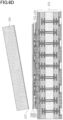
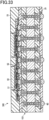
- Fig. 1 is a cross-sectional view illustrating an example of a semiconductor device according to an embodiment of the present invention.
- a first wiring board is an interposer
- a second wiring board is an FC-BGA board.
- a thin first wiring board (which may be termed “interposer” hereinafter) 1 provided with a fine wiring layer formed of only a built-up wiring layer, in which resins and wiring are laminated with each other, is disposed on one surface of a second wiring board (which may be termed “FC-BGA board” hereinafter) 3.
- the first wiring board 101 and the second wiring board 103 are bonded together via junction electrodes, such as solder bumps, copper posts (copper pillars), gold pumps, or the like. These joints will be referred to as interposer-FC-BGA joints 119.
- the gap between the first and second wiring boards 101 and 103 is filled with an underfill 102 as an insulating adhesive material.
- the surface to which semiconductor elements 104 are bonded via copper pillars or solder (the surface facing away from the surface provided with the second wiring board 103) is referred to as a first surface, and portions to which the semiconductor elements 104 are bonded are referred to as semiconductor element-interposer joints 121.
- the gap between each semiconductor element 104 and the first wiring board 101 is filled with an underfill 122.
- the wiring width in the first wiring board (interposer) 1 may be changed as appropriate as long as the wiring can be connected to the signal lines of one or more mounted semiconductor elements 104.
- the first wiring board (interposer) 1 includes an insulating resin layer 112 (see Fig. 5B ) made of photosensitive resins containing one or more of a photosensitive epoxy resin, polyimide resin, and polyamide resin. If a desired wiring width can be obtained, the wiring forming method may be appropriately selected from a damascene process, semi additive process (SAP), and the like.
- the underfill 102 is an adhesive material used for fixing the first and second wiring boards 101 and 103 and sealing the interposer-FC-BGA joints 119.
- the material used for the underfill 102 may be, for example, a material obtained by adding silica, titanium oxide, aluminum oxide, magnesium oxide, zinc oxide, etc. as a filler, to one of an epoxy resin, urethane resin, silicone resin, polyester resin, oxetane resin, and maleimide resin, or a mixture of two or more of these resins.
- the underfill 102 may be formed by filling with a liquid resin.
- the underfill 122 is an adhesive material used for fixing the semiconductor elements 104 and the first wiring board 101 and sealing the semiconductor element-interposer joints 121, and is made of the same material as that of the underfill 102.
- an anisotropically conductive film (ACF) or a non-conductive film (NCF), i.e., a sheet-like film may be disposed in each space in advance before bonding to thereby fill the space when bonding
- NCP non-conductive paste
- a liquid-form resin may be disposed in each space in advance before bonding to thereby fill the space when bonding.
- the first wiring board 101 is sealed with a sealing resin 105 which is a material different from that of the underfill 122 and is obtained by adding silica, titanium oxide, aluminum oxide, magnesium oxide, zinc oxide, etc. as a filler, to one of an epoxy resin, silicone resin, acrylic resin, urethane resin, polyester resin, and oxetane resin, or a mixture of two or more of these resins, which is formed using compression molding, transfer molding, or the like.
- the first wiring board 101 is sealed with the material together with the side surfaces thereof; however, as long as the semiconductor elements 104 are sealed and encapsulated, the design can be appropriately changed. For example, in a mode, the side surfaces of the semiconductor elements 104 may be sealed, while the side surfaces of the first wiring board 101 may not be sealed.
- the intervals between the semiconductor element-interposer joints 121 are smaller than the intervals between the interposer-FC-BGA joints 119. Therefore, in the first wiring board 101, the first surface to which the semiconductor elements 104 are bonded is required to have wiring finer than the surface to which the FC-BGA board is bonded. For example, in order to meet the usage of currently used high bandwidth memories (HBM), the wiring width on the first surface of the first wiring board 101 is required to be around 1 ⁇ m or more and 5 ⁇ m or less.
- HBM high bandwidth memories
- the thickness of one layer including the wiring will be 4 ⁇ m and, with this thickness, two wiring layers may be formed. If the joints between the first and second wiring boards 101 and 103 and the joints between the first wiring board 101 and the semiconductor elements 104 have an electrode thickness of 10 ⁇ m, the total thickness of the first wiring board 101 will be around 28 ⁇ m.
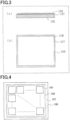
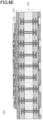
- Fig. 2 is a cross-sectional view illustrating the configuration of a board unit with support according to an embodiment of the present invention.
- the total thickness of the first wiring board 101 is around 28 ⁇ m which is so thin that it is difficult to bond it as it is to the second wiring board 103. Therefore, as shown in Fig. 2 , a support 106 can be effectively used to secure rigidity.
- the rigid support 106 which is less likely to have deformation, is also advantageous for forming the wiring having the width and height of around 2 ⁇ m.
- the first wiring board 101 is formed on the rigid support 106, as shown in Fig. 2 , via a release layer 107, a laser absorption layer 108, and a first seed layer 109. Layers other than the release layer 107, the laser absorption layer 108, and the first seed layer 109 may be provided on the support 106.
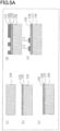
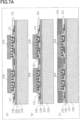
- FIG. 3 is a set of diagrams illustrating a state in which a release layer and a laser absorption layer are formed on a support.
- Fig. 3(a) shows a state in which a release layer 107 and a laser absorption layer 108 are formed on the upper surface of the support 106
- Fig. 3(b) is a plan view illustrating the support 106, the release layer 107, and the laser absorption layer 108 as viewed perpendicularly to the support 106
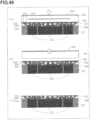
- Fig. 4 is a plan view illustrating a state in which a plurality of second wiring boards are disposed on the support.
- One surface of the support 106 is provided with the release layer 107 and the laser absorption layer 108 which are required when separating the support 106 in the later process.
- the laser absorption layer 108 may be formed into the same planar shape as the release layer 107 but, as shown in Figs. 3(a) and 3(b) , the laser absorption layer 108 does not have to be formed at the peripheral edge portion of the release layer 107.
- the area of the release layer 107 which is not covered with the laser absorption layer 108, as shown in Fig. 3 may be obtained by forming the laser absorption layer 108 on the entire upper surface of the release layer 107, followed by removing part of the laser absorption layer 108 covering the peripheral portion of the release layer 107.
- a protective film may be formed on the peripheral portion of the release layer 107 before forming the laser absorption layer 108, followed by forming a laser absorption layer 108 on the upper surfaces of the release layer 107 and the protective film and further followed by removing the protective film, so that part of the laser absorption layer formed on the upper surface of the protective film is removed, i.e., part of the laser absorption layer is removed from the peripheral portion of the release layer 107.
- the release layer 107 becomes separable due to heat generated when the laser absorption layer 108 absorbs laser, it is preferred that the release layer 107 is in contact with the laser absorption layer 108. If the laser absorption layer 108 has a region contacting the support 106, separation may become difficult and, therefore, the laser absorption layer 108 is formed in a region inside the release layer 107 in plan view. As shown in Fig. 4 , the plurality of first wiring boards 101 on the support 106 are disposed in a region inside the laser absorption layer 108, so that the support 106 can be separated from the first wiring boards 101 with high efficiency.
- a plurality of first wiring boards 101 are disposed on the support 106 to form a board unit formed of the plurality of first wiring boards 101.
- the support 106 described in the present embodiment is a panel that is a rectangular plate-like member. However, the support 106 may be, for example a circular wafer.
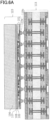
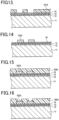
- FIGs. 5A to 5C are each a set of cross-sectional views illustrating an example of a process of producing a board unit with support, according to an embodiment of the present invention.
- a support 106 is prepared.
- the support 106 from which the release layer 107 and the laser absorption layer 108 will be separated using laser light irradiation, is required to have translucency and thus glass, for example, can be used for the support 106.
- Glass has good rigidity and is suitable for forming a fine pattern of the first wiring board 101.
- glass has a low coefficient of thermal expansion (CTE) and is resistant to strain and therefore is excellent in securing pattern placement accuracy and flatness.
- CTE coefficient of thermal expansion
- the thickness of the glass is preferred to be large, e.g., 0.7 mm or more, and more preferred to be 1.1 mm or more, from the perspective of suppressing the occurrence of warpage in the production process.
- the CTE of the glass is preferred to be 3 ppm or more and 15 ppm or less, and is more preferred to be around 9 ppm from the perspective of the CTEs of the second wiring board 103 and the semiconductor elements 104.
- a release layer 107 and a laser absorption layer 108 which are required for separating the support 106 in a later process, are formed in this order on one surface of the support 106.
- the release layer 107 can be selected from, for example, organic resins such as epoxy resins, polyimide resins, polyurethane resins, silicone resins, polyester resins, oxetane resins, maleimide resins, and acrylic resins.
- the release layer 107 may be formed of a plurality of layers, the configuration of which should not be limited by the present embodiment.
- a protective layer may be provided on the release layer 107 for the purpose of protecting the multilayer wiring layer formed on the support 106.
- the method of forming the release layer 107 in the case of using a liquid organic resin can be selected from slit coating, curtain coating, die coating, spray coating, electrostatic coating, inkjet coating, gravure coating, screen printing, gravure offset printing, spin coating, and doctor coating.
- a film-like organic resin lamination, vacuum lamination, vacuum pressing, or the like can be applied.
- release layers 107 are preferred to have a thickness of 10 nm or more. If the thickness is 10 nm or less, the organic resin may be difficult to form. The upper limit of the thickness is limited by the laser light transmittance. Laser light applied from the support 106 side is required to pass through the release layer 107 and reach the laser absorption layer 108. Therefore, the release layer 107 is preferred to transmit 50% or more of infrared laser light, and, from the perspective of reducing laser output, more preferred to transmit 80% or more.
- a material that absorbs infrared light can be selected as a material for the laser absorption layer 108.
- the laser absorption layer 108 can be formed using elements selected from tungsten, molybdenum, titanium, tantalum, niobium, nickel, cobalt, zirconium, zinc, ruthenium, rhodium, palladium, osmium, iridium, and silicon, or alloys or compounds containing these elements.
- the method of forming the laser absorption layer 108 may be vacuum deposition, sputtering, ion plating, MBE, laser ablation, CVD, or the like.
- the laser absorption layer 108 is preferred to have a thickness of 1 nm or more and 500 nm or less. At 1 nm or less, the layer does not function as a continuous film and cannot absorb laser. At 500 nm or more, the load placed on the processing may increase because this layer is removed after separation of the support.
- the thickness is more preferred to be 5 nm or more and 100 nm or less. Considering heat generation due to infrared light absorption, the light absorption rate is preferred to be 50% or more.
- a release layer 107 of 500 nm polyimide resin, and a laser absorption layer 108 of 50 nm titanium can be formed, and glass can be used as the support 106.
- a first seed layer 109 is formed on the laser absorption layer 108 in a vacuum.
- the first seed layer 109 serves as a power supply layer for electroplating when forming wiring.
- the first seed layer 109 can be formed using, for example, sputtering, CVD, or the like, and examples of the material include Cu, Ni, Al, Ti, Cr, Mo, W, Ta, Au, Ir, Ru, Pd, Pt, AlSi, AlSiCu, AlCu, NiFe, ITO, IZO, AZO, ZnO, PZT, TiN, Cu 3 N 4 , and Cu alloys, which can be used singly or in combination of two or more.
- a titanium layer and a copper layer are preferred to be sequentially formed by sputtering.
- the titanium layer secures adhesion with the copper layer, while the copper layer mainly serves as a power supply layer for electroplating.
- the total thickness of the titanium and copper layers is preferred to be 1 ⁇ m or less as a power supply layer for electroplating and thus can be, for example, Ti: 50 nm and Cu: 300 nm.
- the same material i.e., titanium, may be used for them.
- Use of the same material enables removal of all layers together after separation of the support 106, and can simplify the processing.
- a first resist pattern 110 is formed on the first seed layer 109.
- the first resist pattern 110 can be formed using a known photolithography method.
- a conductor layer (first electrodes) 111 is formed by electroplating, followed by removing the first resist pattern 110.
- the conductor layer 111 will be used as electrodes for bonding to semiconductor elements 104 (junction electrodes).
- the junction electrodes are preferred to have a thickness of 5 ⁇ m or more.
- the first surface of the first wiring board 101 is provided with electrodes that can be bonded to at least one semiconductor element.
- the electroplating used for forming the conductor layer 111 may be electroplating of nickel, copper, chromium, Pd, gold, rhodium, iridium, or the like, among which, copper electroplating is preferable from the perspective of ease, cost, and electrical conductivity.
- the thickness of the electroplated copper is preferred to be 1 ⁇ m or more and 30 ⁇ m or less from the perspective of circuit connection reliability, manufacturing cost, and the like.
- the first resist pattern 110 can be removed using a known stripping liquid such as alkaline solvents.
- an insulating resin layer 112 is formed.
- the insulating resin layer 112 is formed so that the conductor layer 111 is embedded therein.
- the insulating resin layer 112 can be formed by, for example, by spin-coating a photosensitive epoxy resin. Photosensitive epoxy resins can be cured at relatively low temperatures, and are less likely to shrink due to curing after formation, and thus are excellent in fine pattern formation thereafter.
- the insulating resin layer 112 can be formed by subjecting an insulating resin film to compression curing using a vacuum laminator. In this case, an insulating film with good flatness can be formed.
- a polyimide may be used as an insulating resin.
- openings are formed in the insulating resin layer 112 using photolithography.
- the openings are formed so as to expose part of the conductor layer 111.
- the openings may be subjected to plasma treatment for the purpose of removing residues produced during development.
- a second seed layer 113 is provided covering the conductor layer 111 exposed in the openings and at least regions of the insulating resin layer 112 in which a conductor layer 115 described later will be formed.
- the second seed layer 113 has a configuration similar to the first seed layer 109 described above, but the configuration as well as the thickness can be changed as appropriate.
- the second seed layer 113 can be formed by sputtering to produce Ti: 50 nm and Cu: 300 nm.
- a second resist pattern 114 is formed on the second seed layer 113, and a conductor layer (wiring layer) 15 is formed by electroplating in the openings of the second resist pattern 114.
- the conductor layer 115 which serves as a wiring layer inside the first wiring board 101, may be formed of copper, for example.
- the second resist pattern 114 is removed. After that, unnecessary portions of the second seed layer 113 are etched away.
- a conductor layer (second electrodes) 16 formed on the outermost surface serves as junction electrodes to the second wiring board 103.
- the junction electrodes are preferred to have a thickness of 5 ⁇ m or more.
- the second surface of the first wiring board 101 is provided with electrodes that can be bonded to the second wiring board (FC-BGA board) 3.
- an outermost surface insulating resin layer 117 is formed on the first wiring board 101, followed by forming openings therein using photolithography to expose at least part of the conductor layer 116.
- the outermost surface insulating resin layer 117 is formed, for example, using a photosensitive epoxy resin.
- the outermost surface insulating resin layer 117 may be made of the same material as that of the insulating resin layer 112.
- a surface treatment layer 118 may be provided to prevent oxidation of the surface of the conductor layer 116 and enhance wettability of solder bumps.
- the surface treatment layer 118 may be formed by Ni/Pd/Au electroless plating. It should be noted that an OSP (surface treatment using organic solderability preservative water-soluble preflux) film may be formed as the surface treatment layer 118.
- Plating may be appropriately selected from tin electroless plating, Ni/Au electroless plating, and other electroplating methods according to the application.
- a solder material is mounted on the surface treatment layer 118, melted, cooled, and fixed to obtain solder bumps as interposer-FC-BGA joints 119a on the first wiring board 101 side.
- a board unit 123 with support that is, a first wiring board (interposer) 1 formed on the support 106, is completed.
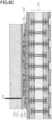
- FIGs. 6A to 6E are cross-sectional views illustrating an example of a method of producing a board unit according to an embodiment of the present invention.
- solder bumps as interposer-FC-BGA joints 119b on the second wiring board 103 side are designed.
- the first wiring board 101 formed on the support 106 is placed on the second wiring board 103 as produced and, as shown in Fig. 6B , the first wiring board 101 formed on the support 106 and the second wiring board 103 are bonded together, followed by filling an underfill 102 therebetween to fix the first and second wiring boards 101 and 103 and seal the interposer-FC-BGA joints 119.
- laser light 120 is applied to the laser absorption layer 108 formed at the interface with the release layer 107, from the rear surface of the support 106, i.e., from the surface of the support 106 facing away from the surface provided with the first wiring board 101.
- the release layer 107 is decomposed by the heat generated due to the laser absorption layer 108 absorbing the laser light 120, and the release layer 107 and the laser absorption layer 108 are brought into a separable state.
- the support 106 can be detached.
- the laser absorption layer 108 and the first seed layer 109 are removed to obtain a board as shown in Fig. 6E .
- this layer can be dissolved and removed using an alkaline etching agent.
- the first seed layer 109 is titanium, this layer can be simultaneously dissolved and removed.
- the remaining copper layer of the first seed layer 109 can be dissolved and removed using an acid-based etching agent. In this way, the first wiring board (interposer) 1 and the second wiring board (FC-BGA board) 3 are bonded together.
- the conductor layer 111 exposed to the surface may be surface-treated using Ni/Pd/Au electroless plating, OSP, tin electroless plating, Ni/Au electroless plating, or the like to prevent oxidation and enhance wettability of the solder bumps.
- a board unit 124 from which the support has been removed is completed.
- the semiconductor elements 104 are bonded to the board unit 124 from which the support has been removed, and the underfill 122 is filled to fix the semiconductor elements 104 and the first wiring board 101 and to seal the semiconductor element-interposer joints 121, followed by sealing the semiconductor elements 104 with the sealing resin 105 to complete the semiconductor device 125.
- the method of producing the first wiring board 101 on the support 106 is similar between the first and second embodiments.
- the first wiring board 101 is separated from the support 106 and then bonded to the second wiring board 103, followed by bonding the semiconductor elements 104.
- the second embodiment is different from the first embodiment in that the semiconductor elements 104 are bonded to the first wiring board 101 formed on the support 106, and then the first wiring board 101 is separated together with the semiconductor elements 104 from the support 106, followed by bonding the first wiring board 101 together with the semiconductor elements 104 to the second wiring board 103.
- the surface facing away from the surface provided with the support 106 is the second surface of the first wiring board 101, and electrodes for bonding to the second wiring board 103 are provided to this second surface, while the support 106-side surface is the first surface of the first wiring board 101, and the electrodes for bonding to the semiconductor elements 104 are provided to this first surface.
- the surface facing away from the surface provided with the support is the first surface of the first wiring board 101, and electrodes for bonding to the semiconductor elements 104 are provided to this second surface
- the support-side surface is the second surface of the first wiring board 101, and the electrodes for bonding to the second wiring board 103 are provided to this second surface.
- FIGS. 7A, 7B and 8 each show a set of cross-sectional views illustrating an example of a method of producing a semiconductor device according to an embodiment of the present invention.
- FIG. 8 is a cross-sectional view illustrating an example of a semiconductor device according to an embodiment of the present invention.
- the semiconductor elements 104 are bonded to the surface of the first wiring board 101 facing away from the surface provided with the support 106, via copper pillars or solder. These joints are referred to as semiconductor element-interposer joints 121.
- an underfill 122 is filled in the vicinity of the semiconductor element-interposer joints 121 to fix the semiconductor elements 104 and the first wiring board 101 and to seal the semiconductor element-interposer joints 121.
- a sealing resin 105 is formed to seal the semiconductor elements 104.
- the sealing resin 105 which is different from the material of the underfill 122, is obtained by adding silica, titanium oxide, aluminum oxide, magnesium oxide, zinc oxide, etc. as a filler, to one of an epoxy resin, silicone resin, acrylic resin, urethane resin, polyester resin, and oxetane resin, or a mixture of two or more of these resins, and is formed using compression molding, transfer molding, or the like.
- the support 106 is separated.
- laser light 120 is applied to the laser absorption layer 108 to separate the first wiring board 101, to which the semiconductor elements are mounted, from the support 106.
- the laser light 120 is applied to the laser absorption layer 108 formed at the interface with the support 106, from the rear surface of the support 106, i.e., from the surface of the support 106 facing away from the surface provided with the semiconductor elements 104.
- the heat generated due to the laser absorption layer 108 absorbing the laser light 120 decomposes the release layer 107 and brings it into a separable state, so that, as shown in Fig. 7B(e) , the support 106 can be detached.
- the laser absorption layer 108 and the first seed layer 109 are removed.
- titanium is used for the laser absorption layer 108, and in this case, the laser absorption layer 108 can be dissolved and removed using an alkaline etching agent.
- the first seed layer 109 is titanium, the laser absorption layer 108 and the first seed layer 109 can be simultaneously dissolved and removed.
- the remaining copper layer of the first seed layer 109 can be dissolved and removed using an acid-based etching agent.
- a semiconductor device 126 in which the first wiring board (interposer) 1 and the semiconductor elements 104 are bonded together can be obtained.
- the conductor layer 111 exposed to the surface may be surface-treated using Ni/Pd/Au electroless plating, OSP, tin electroless plating, Ni/Au electroless plating, or the like to prevent oxidation and enhance wettability of the solder bumps to provide a semiconductor device 126.
- the semiconductor device 126 is bonded to the second wiring board (FC-BGA substrate ) 3 and an underfill 102 is filled therebetween to fix the semiconductor device 126 and the second wiring board 103 and to seal the interposer-FC-BGA joints 119, thereby completing the semiconductor device 125 integrated with the first wiring board 101.
- the release layer and the laser absorption layer are provided in this order in the method in which a wiring board is formed on a support via a release layer, and the wiring board is separated thereafter from the support.
- a board unit with support which facilitates separation of the wiring board, does not require a high-energy UV laser and which is less likely to form residues of the release layer after separation of the support, a board unit, a semiconductor device, a board unit with support, and a method of producing them.
- the present embodiment has an aim of providing a wiring board with support in which the support can be easily separated from the wiring board.
- Functional devices refers to devices which are activated with a supply of electrical power and/or electrical signals, devices which output electrical power and/or electrical signals due to stimulation from outside, or devices which are activated with a supply of electrical power and/or electrical signals and which output electrical power and/or electrical signals due to stimulation from outside.
- Functional devices may be, for example, in the forms of chips, such as semiconductor chips or chips in which circuits or elements are formed on a substrate, such as a glass substrate, made of a material other than semiconductor materials.
- Functional devices can include, for example, one or more from among large-scale integrated circuits (LSIs), memories, imaging devices, light-emitting devices, and microelectromechanical systems (MEMSs).
- MEMSs may include, for example, one or more from among pressure sensors, acceleration sensors, gyro sensors, tilt sensors, microphones, and acoustic sensor.
- functional devices may be semiconductor chips including LSIs.
- Fig. 9 is a schematic cross-sectional view illustrating a wiring board with support, according to an embodiment of the present invention.
- a wiring board 1 with support shown in Fig. 9 includes a support 11, light absorption layer 12, a release layer 13, a first seed layer 14, a wiring board 15, an outermost surface insulating layer 16, a surface treatment layer 17, and first metal bumps 18.
- the wiring board 1 with support is used for, for example, transferring the wiring board 15 to an FC-BGA board. The transfer is performed by, for example, applying laser light to the light absorption layer 12, and separating the support 11 from the wiring board 15.
- the support 11 has a support surface, and transmits light with a specific wavelength in the direction perpendicular to the support surface.
- the support 11 may have transparency, for example.
- the specific wavelength may be, for example, in the ultraviolet or infrared wavelength region. If the specific wavelength is in the ultraviolet wavelength region, the specific wavelength may be, for example, in the range of 150 nm to 400 nm. If the specific wavelength is in the infrared wavelength region, the specific wavelength may be, for example, in the range of 700 nm to 2,000 nm.
- the material of the support 11 may be, for example, glass, polycarbonate, or acrylic or silicone material. Silicone can be used if the specific wavelength is in the infrared wavelength region.
- the material of the support 11 is preferred to be glass. If the support 11 is made of glass, the support 11 with a sufficient thickness can be excellent in shape retention. Using such a support 11, a wiring board 15 having a fine wiring pattern can be easily formed.
- the glass is preferred to have a coefficient of linear expansion (CTE: coefficient of thermal expansion) in the range of 3 ppm or more and 15 ppm or less, and more preferred to be in the range of 3.3 ppm to 12.6 ppm. If the coefficient of linear expansion is in the range of 3 ppm or more and 15 ppm or less, the wiring pattern can be easily arranged with high accuracy in the wiring board 15, and a flat wiring pattern 15 can be easily formed. If the coefficient of linear expansion of the glass is around 9 ppm, it is approximate to the coefficient of linear expansion of FC-BGA boards and that of semiconductor chips and, therefore, is less likely to cause warpage or the like.
- CTE coefficient of thermal expansion
- the thickness of the support 11 is preferred to be 0.7 mm or more, and is more preferred to be 1.1 mm or more. If the support 11 is excessively thin, warpage tends to occur. If the support 11 is excessively thick, laser light absorption by the support 11 tends to increase. If the support 11 is made of glass and the thickness thereof is in the above range, warpage is less likely to occur in the production process.
- the support 11 may have a rectangular or circular shape.
- the light absorption layer 12 is interposed between the support 11 and the release layer 13. Compared to the release layer 13, the light absorption layer 12 exhibits higher light absorbance. The light absorption layer 12 generates heat by absorbing light having the above specific wavelength, and transfers the heat to the release layer 13.
- Materials used for the light absorption layer 12 may be metals, for example. These metals are preferred to have an attenuation coefficient in the range of 3.3 to 5.32 at any wavelength in the range of 1,033 nm to 1,079 nm. Examples of the metals having an attenuation coefficient in the above range include titanium, chromium, tungsten, nickel, molybdenum, niobium, and tantalum.
- the attenuation coefficient can be measured, for example, using spectroscopic ellipsometry.
- the metals are preferred to have a refractive index in the range of 0.96 to 3.35, and more preferably in the range of 2.29 to 3.35, at any wavelength in the range of 1,033 nm to 1,079 nm.
- Examples of the metals having the refractive index in the range of 0.96 to 3.35 include titanium, chromium, tungsten, nickel, molybdenum, niobium, and tantalum.
- Examples of the metals having the refractive index in the range of 2.29 to 3.35 include titanium, chromium, tungsten, nickel, and molybdenum.
- the refractive index can be measured, for example, using spectroscopic ellipsometry.
- the materials of the light absorption layer 12 are preferred to have an attenuation coefficient in the range of 3.3 to 5.31 at any wavelength in the range of 1,033 nm to 1,079 nm, and to have a refractive index in the range of 0.96 to 3.35 at any wavelength in the range of 1,033 nm to 1,079 nm.
- examples of such materials include titanium, chromium, tungsten, nickel, molybdenum, niobium, and tantalum.
- Table 1 shows attenuation coefficients and refractive indices in any of wavelength in the range of 1,033 nm to 1,079 nm for titanium, chromium, tungsten, niobium, molybdenum, niobium, and tantalum.
- Examples of the materials of the light absorption layer 12 include one or more metals selected from the group consisting of titanium, chromium, tungsten, nickel, molybdenum, niobium, and tantalum, and alloys or compounds containing these metals. It is preferred that the materials of the light absorption layer 12 are one or more metals selected from the group consisting of titanium, chromium, tungsten, nickel, and molybdenum, or alloys or compounds containing these metals. It is more preferred that the materials of the light absorption layer 12 are titanium, or alloys or compounds containing titanium.
- the light absorption layer 12 can be formed, for example, using vacuum deposition such as molecular beam epitaxy (MBE), sputtering, ion plating, laser abrasion, or chemical vapor deposition (CVD).
- vacuum deposition such as molecular beam epitaxy (MBE), sputtering, ion plating, laser abrasion, or chemical vapor deposition (CVD).
- the thickness of the light absorption layer 12 is preferred to be in the range of 1 nm to 500 nm, and is more preferred to be in the range of 5 nm to 100 nm. If the light absorption layer 12 is excessively thin, it cannot sufficiently absorb laser light when the wiring board 1 with support is irradiated with laser light and, therefore, it will be difficult to separate the support 11 from the wiring board 15 with ease. If the light absorption layer 12 is excessively thick, heat generated when the light absorption layer 12 is irradiated with laser light tends to transfer in the in-plane direction of the light absorption layer 12 from the irradiated area and, therefore, the irradiated area is less likely have sufficiently high temperatures.
- the release layer 13 is interposed between the support 11 and the wiring board 15.
- the release layer 13 decreases adhesion in response to heating. "To decrease adhesion” refers to the release layer 13 being separated from the light absorption layer 12, or the force required for separating the release layer 13 and the light absorption layer 12 decreasing.
- Examples of the materials of the release layer 13 include resins such as epoxy resins, polyimide resins, polyurethane resins, silicone resins, polyester resins, oxetane resins, maleimide resins, and acrylic resins.
- resins such as epoxy resins, polyimide resins, polyurethane resins, silicone resins, polyester resins, oxetane resins, maleimide resins, and acrylic resins.
- a polyimide resin for example, UPIA (trademark) manufactured by UBE Corporation can be used.
- the thickness of the release layer 13 is preferred to be, for example, in the range of 10 nm to 50 ⁇ m, more preferred to be in the range of 10 nm to 1 ⁇ m, and even more preferred to be in the range of 10 nm to 0.5 ⁇ m. If the release layer 13 is excessively thin, it will be difficult to form the release layer 13 uniformly. If the release layer 13 is excessively thick, it will be difficult to form a wiring board 15 having good flatness.
- the release layer 13, if a liquid resin is used as a material therefor, can be formed, for example, using slit coating, curtain coating, die coating, spray coating, electrostatic coating, inkjet coating, gravure coating, screen printing, gravure offset printing, spin coating, or doctor coating.
- the release layer 13, if a film-shaped resin is used as a material therefor, can be provided on the light absorption layer 12 using, for example, lamination, vacuum lamination, or vacuum pressing.
- the release layer 13 may be formed of two or more layers.
- the first seed layer 14 may be, for example, a power supply layer when forming a conductor layer described later.
- the first seed layer 14 may contain, for example, copper, nickel, aluminum, titanium, chromium, molybdenum, tungsten, tantalum, gold, iridium, ruthenium, palladium, platinum, Al-Si alloys, Al-Si-Cu alloys, Al-Cu alloys, Ni-Fe alloys, indium tin oxide (ITO), indium zinc oxide (IZO), active zinc oxide (AZO), zinc oxide (ZnO), piezoelectric zirconate titanate (PZT), titanium nitride (TiN), Cu 3 N 4 , or Cu alloys, singly or as a mixture thereof.
- ITO indium tin oxide
- IZO indium zinc oxide
- AZO active zinc oxide
- ZnO zinc oxide
- PZT piezoelectric zirconate titanate
- TiN titanium nitride
- the first seed layer 14 may be formed, for example, using sputtering or chemical vapor deposition (CVD).
- the thickness of the first seed layer 14 is preferred to be 1 ⁇ m or less, and is more preferred to be in the range of 50 nm to 500 nm.
- the first seed layer 14 may be formed of two or more layers.
- the seed layer 14 may be formed of, for example, a first metal-containing layer interposed between the release layer 13 and the wiring board 15, and a second metal-containing layer interposed between the first metal-containing layer and the wiring board 15.
- the first metal-containing layer may contain titanium, for example.
- the second metal-containing layer may contain copper, for example.
- the first and second metal-containing layers may be formed using sputtering, for example. If a first metal-containing layer containing titanium is used, the first metal-containing layer may have good adhesion to the release layer 13. If a second metal-containing layer containing copper is used, the second metal-containing layer may have good adhesion to the first metal-containing layer and the conductor layer described later.
- the thickness of the first metal-containing layer is preferred to be, for example, in the range of 10 nm to 100 nm.
- the thickness of the second metal-containing layer is preferred to be, for example, in the range of 40 nm to 400 nm.
- the wiring board 15 faces the support surface of the support 11.
- the wiring board 15 may connect between, for example, functional devices, such as semiconductor chips, and an FC-BGA board.
- the wiring board 15 may be produced using a known method, for example.
- the wiring board 15 may be, for example, a multilayer wiring board such as an interposer.
- the wiring board 15 may be formed of, for example, a built-up wiring layer.
- the wiring board 15 may include, for example, a fine wiring pattern.
- the minimum line/space width in the wiring board 15 may be, for example, in the range of 1 ⁇ m/1 ⁇ m to 5 ⁇ m/5 ⁇ m.
- the conductor layer included in the wiring board 15 may be formed, for example, using a damascene method or semi-additive method. The conductor layer will be described later.
- a protective layer may be provided between the release layer 13 and the wiring board 15.
- a support 11 is prepared.
- the support 11 is assumed to be made of glass.
- a light absorption layer 12 and a release layer 13 are formed on the support 11. Specifically, first, titanium is sputtered on the support 11. Thus, a light absorption layer 12 is formed. Next, a polyimide resin is applied onto the light absorption layer 12 using spin coating. Thus, a release layer 13 is formed.
- a first seed layer 14 is formed on the release layer 13.
- a first metal-containing layer and a second metal-containing layer are formed as a first seed layer 14.
- titanium is sputtered on the release layer 13.
- a first metal-containing layer is formed.
- copper is sputtered on the first metal-containing layer.
- a second metal-containing layer is formed.
- a resist layer 151A is formed in a pattern on the first seed layer 14. Specifically, first, a resist layer 151A is formed on the first seed layer 14 in a vacuum. After that, part of the resist layer 151A is removed using photolithography to provide openings. Thus, a resist layer 151A is formed in a pattern.
- Materials for the resist layer 151A may be, for example, alkaline developable photosensitive resins.
- a conductor layer 152A is formed on the first seed layer 14. Specifically, first, a conductor layer 152A containing copper is formed on the first seed layer 14, i.e., portions thereof not covered with the resist layer 151A, using electroplating. After that, the resist layer 151A is removed using a resist stripping liquid such as an alkaline solution. Thus, a conductor layer 152A is formed.
- the conductor layer 152A may serve as electrodes, for example.
- the conductor layer 152A may serve, for example, as electrodes used for bonding to the first wiring board described later, or electrodes used for bonding to functional devices.
- the conductor layer 152A contains copper, the conductor layer 152A can be formed easily at low cost.
- the conductor layer 152A containing copper have good electrical conductivity.
- the conductor layer 152A may be formed of, for example, nickel, chromium, palladium, gold, or rhodium.
- the conductor layer 152A may be formed, for example, using electroplating.
- the thickness of the conductor layer 152A is preferred to be in the range of 1 ⁇ m to 30 ⁇ m, and is more preferred to be in the range of 1 ⁇ m to 5 ⁇ m. If the conductor layer 152A is excessively thick, the production cost tends to increase. If the conductor layer 152A is excessively thin, problems may occur when bonding between the functional devices or the first wiring board described later and the wiring board 15.
- an insulating layer 153A is formed on the first seed layer 14, i.e., portions thereof not covered with the conductor layer 152A, and on the surface of the conductor layer 152A.
- a photosensitive epoxy resin is applied to portions of the first seed layer 14 not covered with the conductor layer 152A and to the surface of the conductor layer 152A using spin coating. After that, the photosensitive epoxy resin is cured.
- an insulating layer 153A is formed.
- the insulating layer 153A may be formed, for example, so that the conductor layer 152A is embedded in the insulating layer 153A.
- the insulating layer 153A can be easily cured at comparatively low temperatures. Photosensitive epoxy resins are less likely to shrink due to curing and thus are excellent in forming fine wiring patterns.
- Materials used for the insulating layer 153A may be polyimide resins or polyamide resins.
- the insulating layer 153A may be obtained by pressing an insulating resin film using a vacuum laminator. In this case, an insulating layer 153A having good flatness can be formed.
- the thickness of the insulating layer 153A is preferred to be in the range of 0.5 ⁇ m to 50 ⁇ m, and is more preferred to be in the range of 2 ⁇ m to 15 ⁇ m. If the insulating layer 153A is excessively thick, it will be difficult to obtain a wiring board 15 having good flatness. If the insulating layer 153A is excessively thin, it will be difficult to achieve high insulation reliability.
- one or more openings are formed in the insulating layer 153A using photolithography.
- the openings are formed so as to expose part of the upper surface of the conductor layer 152A.
- plasma treatment may be performed to remove the residues formed in the openings due to development.
- a second seed layer 154A is formed on the conductor layer 152A exposed in the openings and on the surface of the insulating layer 153A.
- the second seed layer 154A may contain, for example, copper, nickel, aluminum, titanium, chromium, molybdenum, tungsten, tantalum, gold, iridium, ruthenium, palladium, platinum, Al-Si alloys, Al-Si-Cu alloys, Al-Cu alloys, Ni-Fe alloys, indium tin oxide (ITO), indium zinc oxide (IZO), active zinc oxide (AZO), zinc oxide (ZnO), piezoelectric zirconate titanate (PZT), titanium nitride (TiN), Cu 3 N 4 , or Cu alloys, singly or as a mixture of them.
- ITO indium tin oxide
- IZO indium zinc oxide
- AZO active zinc oxide
- ZnO zinc oxide
- PZT piezoelectric zirconate titanate
- TiN titanium nitride
- Cu 3 N 4 or Cu alloys, singly or as a mixture of them.
- the second seed layer 154A may be formed, for example, using sputtering or chemical vapor deposition (CVD).
- the thickness of the second seed layer 154A is preferred to be 1 ⁇ m or less, and is more preferred to be in the range of 50 nm to 500 nm.
- the second seed layer 154A may be formed of two or more layers.
- the second seed layer 154A may be formed of, for example, a first metal-containing layer provided on the conductor layer 152A and the insulating layer 153A, and a second metal-containing layer provided on the conductor layer 152A and the insulating layer 153A via the first metal-containing layer.
- the first metal-containing layer may contain titanium, for example.
- the second metal-containing layer may contain copper, for example.
- the first and second metal-containing layers may be formed using sputtering, for example.
- the second seed layer 154A is assumed to be formed of a first metal-containing layer containing titanium and a second metal-containing layer containing copper. Furthermore, the first and second metal-containing layers are assumed to have respective thicknesses of 50 nm and 300 nm.
- a resist layer 151B is formed in a pattern on the second seed layer 154A. Specifically, openings are formed in the resist layer 151B so as to expose portions of the second seed layer 154A adjacent to the conductor layer 152A. After that, a conductor layer 152B is formed so as to cover the entire regions of the surface of the second seed layer 154A not covered with the resist layer 151B.
- the conductor layer 152B is a wiring pattern included in the wiring board 15.
- the materials and forming methods described for the resist layer 151A apply to the resist layer 151B.
- the materials and forming methods described for the conductor layer 152A apply to the conductor layer 152B and the conductor layer 152C described later.
- the conductor layer 152B is assumed to contain copper.
- the resist layer 151B is removed. After that, portions of the second seed layer 154A not covered with the conductor layer 152B are etched away.
- the structure shown in Fig. 20 includes conductor layers 152A, 152B, 152C and 152D, insulating layers 153A, 153B and 153C, and second seed layers 154A, 154B and 154C.
- the conductor layers 152B and 152C may serve as, for example, wiring of the wiring board 15.
- the conductor layer 152D may serve as, for example, electrodes used for bonding to the first wiring board described later, or electrodes used for bonding to the functional devices.
- the conductor layer 152D is preferred to have a thickness of 5 ⁇ m or more. Thus, a wiring board 15 is formed.
- the number of times of repeating the methods described referring to Figs. 15 to 19 may be one, or three or more.
- an outermost surface insulating layer 16 is formed in a pattern on the wiring board 15. Specifically, first, an outermost surface insulating layer 16 is formed in the regions of the surface of the insulating layer 153C not covered with the second seed layer 154C and the conductor layer 152D, on the surface of the conductor layer 152D, and on the side surfaces of the second seed layer 154C. Next, openings are formed in the outermost surface insulating layer 16 using photolithography to expose at least part of the conductor layer 152D.
- Materials of the outermost surface insulating layer 16 may be, for example photosensitive epoxy resins. Materials of the outermost surface insulating layer 16 may be the same as the materials of the insulating layer 153A.
- a surface treatment layer 17 is formed covering portions of the conductor layer 152D not covered with the outermost surface insulating layer 16.
- the surface treatment layer 17 is provided, for example, to prevent oxidation of the surface of the conductor layer 152D and/or to improve wettability of the first metal bumps 18.
- a plating film such as of Ni/Pd/Au electroless plating, tin electroless plating, and Ni/Au electroless plating may be used.
- a water-soluble preflux (organic solderability preservative (OSP)) film may be used as the surface treatment layer 17.
- first metal bumps 18 are formed on the surface treatment layer 17. Specifically, for example, the material of the first metal bumps 18 is disposed on the surface treatment layer 17 and fixed by melting and cooling to form the first metal bumps 18.
- Examples of the material of the first metal bumps 18 include Sn-Ag-Cu alloys, Sn-Ag alloys, and Sn-Cu alloys.
- the outermost surface insulating layer 16, the surface treatment layer 17, and the first metal bumps 18 may be omitted.
- the wiring width of the wiring board 15 is preferred to be, for example, in the range of 1 ⁇ m or more and 5 ⁇ m or less.
- the wiring board 15 can be used as interposers included in high-bandwidth memories (HBMs). For example, if the wiring width is 2 ⁇ m, the wiring height is 2 ⁇ m, and the thickness of each insulating layer is 2 ⁇ m, the thickness of the layer formed of an insulating layer and a conductor layer is 4 ⁇ m.
- the thickness of the laminate formed of the wiring board 15 and the conductor layers 152A and 152D will be 28 ⁇ m.
- the laminate formed of the wiring board 15 and the conductor layers 152A and 152D may be thin.
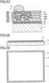
- Fig. 24 is a schematic cross-sectional view illustrating a wiring board 1 with support omitting the wiring board 15, the outermost surface insulating layer 16, the surface treatment layer 17, and the first metal bumps 18 from the wiring board 1 with support described above.
- Fig. 25 is a schematic plan view illustrating a release layer 13-side surface of the wiring board 1 with support illustrated in Fig. 24 .
- the outline of the first orthogonal projection of the release layer 13 onto the plane parallel to the support surface of the support 11 is preferred to be inside the outline of the second orthogonal projection of the light absorption layer 12 onto the plane. If the outline of the first orthogonal projection is inside the outline of the second orthogonal projection, heat generated in the light absorption layer 12 due to laser light irradiation is easily transferred to the entire release layer 13. Accordingly, the support 11 can be easily separated from the wiring board 15. Therefore, for example, in the case where the wiring board 15 is transferred to an FC-BGA board using the wiring board 1 with support to obtain a composite wiring board, composite wiring boards can be obtained with high productivity.
- the structure shown in Figs. 24 and 25 can be obtained by forming a release layer 13 and then removing the peripheral portion of the release layer 13.
- the structure shown in Figs. 24 and 25 can be obtained by forming a light absorption layer 12, then forming a protective film on the peripheral portion of the light absorption layer 12, then forming a release layer 13 on the light absorption layer 12 and the protective film, and then removing the protective film to remove the peripheral portion of the release layer 13 on the protective film.
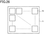
- Fig. 26 is a schematic plan view illustrating a wiring board 1 with support omitting the outermost surface insulating layer 16, the surface treatment layer 17, and the first metal bumps 18 from the wiring board 1 with support described above.
- Fig. 26 shows the wiring board 15-side surface of the wiring board 1 with support.
- a plurality of wiring boards 15 may be provided to the wiring board 1 with support.
- the plurality of wiring boards 15 may form a board unit, for example.
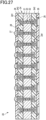
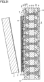
- Figs. 27 to 31 an example of a method of producing a composite wiring board will be described. It should be noted that the surface treatment layer 17 is omitted from Figs. 28 to 32 .
- the first wiring board 20 includes a core layer 21, a conductor material 22, an insulating resin 23, a layer 24, electrodes 25, an outermost surface insulating resin layer 26, and second metal bumps 27.
- the first wiring board 20 may be an FC-BGA board, for example.
- the core layer 21 is an insulating layer.
- the core layer 21 may be, for example, a fiber-reinforced substrate obtained by impregnating a thermosetting insulating resin in a woven or non-woven fabric.
- a thermosetting insulating resin obtained by impregnating a thermosetting insulating resin in a woven or non-woven fabric.
- the woven or non-woven fabric for example, glass fibers, carbon fibers, or aramid fibers can be used.
- the insulating resin epoxy resins can be used, for example.
- the core layer 21 is provided with one or more through holes.
- the side walls of the through holes are covered with the conductor material 22 containing metals such as copper.
- the through holes covered with the conductor material 22 are filled with the insulating resin 23.
- the support surfaces of the core layer 21 are provided with respective layers 24.
- the layers 24 each include conductor patterns 241 and an insulating layer 242.
- the conductor patterns 241 are in contact with the conductor material 22.
- the insulating layer 242 may cover, for example, the side surfaces of the conductor patterns 241.
- portions that are not covered with the insulating layer 242 and are not in contact with the core layer 21 are provided with respective electrodes 25.
- the line/space in each layer 24 may be, for example, in the range of 8 ⁇ m/8 ⁇ m to 25 ⁇ m/25 ⁇ m.
- the second metal bumps 27 are provided on the respective electrodes 25.
- the outermost surface insulating resin layer 26 covers the surface of the layer 24, the side surfaces of the electrodes 25, and part of the second metal bumps 27.
- the arrangement of the second metal bumps 27 may be similar, for example, to the arrangement of the first metal bumps 18 provided to the wiring board 1 with support shown in Fig. 9 .
- the materials described for the first metal bumps 18 of the wiring board 1 with support can be used.
- an outermost surface insulating resin layer 26 is provided to the surfaces of the electrodes 25 and the surface of the layer 24, with part of the surfaces of the electrodes 25 exposed.
- the first wiring board 20 is aligned with the wiring board 1 with support shown in Fig. 9 .
- the alignment between the first wiring board 20 and the wiring board 1 with support is performed so that the second metal bumps 27 provided to the first wiring board 20 align with the respective first metal bumps 18 provided to the wiring board 1 with support shown in Fig. 9 .
- the first wiring board 20 is bonded to the wiring board 15 as a second wiring board included in the wiring board 1 with support, and then a first underfill 31 is filled in portions between the first wiring board 20 and the wiring board 1 with support.
- the first wiring board 20 and the wiring board 1 with support are bonded together so as to face each other.
- the first wiring board 20 is bonded to the wiring board 1 with support so as to face the wiring board 15-side surface of the wiring board 1 with support.
- the bonding is performed via the second metal bumps 27 provided to the first wiring board 20 and the first metal bumps 18 provided to the wiring board 1 with support. Through this bonding, first joints 30 are formed.
- the material that can be used for the underfill 31 may be, for example, a mixture of one or more resins selected from the group consisting of epoxy resins, urethane resins, silicone resins, polyester resins, oxetane resins, and maleimide resins, with a filler such as silica, titanium oxide, aluminum oxide, magnesium oxide, or zinc oxide.
- laser light 40 is applied to the light absorption layer 12.
- the laser light 40 is applied to the light absorption layer 12 from the support 11-side surface of the composite of the first wiring board 20 and the wiring board 1 with support.
- the white arrow in Fig. 30 indicates the direction of the laser light 40.
- the laser light 40 has a specific wavelength.
- the specific wavelength is, for example, in the ultraviolet or infrared wavelength region. If the specific wavelength is in the ultraviolet wavelength region, the specific wavelength may be, for example, in the range of 150 nm to 400 nm. If the specific wavelength is in the infrared wavelength region, the specific wavelength may be, for example, in the range of 700 nm to 2,000 nm.
- the laser light 40 is preferred to be in the infrared wavelength region.
- the laser light 40 in the infrared wavelength region is less likely to damage the wiring board 15, compared to the laser light 40 in the ultraviolet wavelength region.
- the conductor layers 152A, 152B, 152C and 152D or the insulating layers 153A, 153B and 153C are prone to defects.
- the output of the laser light 40 is preferred to be in the range of 0.05 W to 25 W, and is more preferred to be in the range of 0.1 W to 10 W. If the output of the laser light 40 is in the above range, damage is less likely to occur in the wiring board 15. If the output of the laser light 40 is excessively large, damage tends to occur in the wiring board 15. If the output of the laser light 40 is excessively small, it will be difficult to separate the support 11 from the wiring board 15.
- the irradiation energy of the laser light 40 per unit area is preferred to be in the range of 1 mJ/cm 2 to 1,000 mJ/cm 2 , and is more preferred to be in the range of 10 mJ/cm 2 to 300 mJ/cm 2 .
- the number of times of irradiation of the laser light 40 is preferred to be one. Irradiation may be performed multiple times. From the perspective of processing load, fewer irradiations are preferred.
- the light absorption layer 12 when it is irradiated with the laser light 40, generates heat.
- the heat generated in the light absorption layer 12 is transferred to the release layer 13, the release layer 13 contacting the light absorption layer 12 is altered at positions of the light absorption layer 12 irradiated with the laser light 40. As a result, adhesion of the release layer 13 decreases.
- the support 11 and the light absorption layer 12 are separated from the wiring board 15.
- the release layer 13 and the first seed layer 14 are removed.
- the release layer 13 is removed, according to an example, by dry etching using O 2 or CF 2 plasma. According to another example, the release layer 13 is removed using a hydrazine or strong alkaline etching liquid. The release layer 13 is preferred to be removed by dry etching.
- the first metal-containing layer 14 is formed of a first metal-containing layer of titanium and a second metal-containing layer of copper
- the first metal-containing layer may be removed, for example, using an alkaline etching agent
- the second metal-containing layer may be removed, for example, using an acid-based etching agent.
- a surface treatment layer 17 may be formed on the surface of the conductor layer 152A.
- separation was caused at the interface between the light absorption layer 12 and the release layer 13 in the method described above, separation may be caused at the interface between the release layer 13 and the first seed layer 14.
- the composite wiring board 100 described above can be used, for example, for producing packaged devices.
- Packaged devices may include, for example, the first wiring board 20, the wiring board 15, and functional devices described above.
- Fig. 33 a method of producing a packaged device that uses the composite wiring board 100 will be described.
- the functional devices may be, for example, semiconductor chips or chips, such as chips in which circuits or elements are formed on a substrate, such as a glass substrate, made of a material other than semiconductor materials.
- the functional devices are assumed to be semiconductor chips.
- the packaged device herein is a semiconductor package.
- the composite wiring board 100 and functional devices 50 are bonded together.
- the functional devices 50 and the composite wiring board 100 are bonded together so as to face each other.
- the functional devices 50 are bonded to the composite wiring board 100 so as to face the wiring board 15-side surface of the composite wiring board 100.
- the functional devices 50 are bonded to the composite wiring board 100 via second joints 51. Specifically, the functional devices 50 are bonded to the conductor layer 152D via the second joints 51. Herein, the functional devices 50 are bonded to the composite wiring board 100 using flip chip bonding. One or more functional devices 50 may be bonded to the composite wiring board 100 using other bonding methods such as wire bonding.
- the second joints 51 are arrayed at a narrow pitch between each functional device 50 and the composite wiring board 100.
- the second joints 51 may be, for example, pillars made of copper, or solders. If the functional devices 50 are bonded to the composite wiring board 100 using wire bonding, the functional devices 50 and the composite substrate 100 can be electrically connected using gold wires.
- a second underfill 52 is filled in portions between the functional devices 50 and the composite wiring board 100.
- Materials of the second underfill 52 may be similar, for example, to the materials described for the first underfill 31.
- the material that can be used for the sealing resin 53 may be, for example, a mixture of one or more resins selected from the group consisting of epoxy resins, urethane resins, silicone resins, polyester resins, oxetane resins, and maleimide resins, with a filler such as silica, titanium oxide, aluminum oxide, magnesium oxide, and zinc oxide.
- the material of the sealing resin 53 is preferred to be different from the material of the second underfill 52.
- the sealing resin 53 can be formed using, for example, compression molding or transfer molding.
- third metal bumps 60 are formed in the regions where the electrodes 25 are exposed on the surface of the first wiring board 20 of the composite wiring board 100.
- the third metal bumps 60 are used, for example, for bonding to a mother board.
- Materials of the third metal bumps 60 may be similar, for example, to the materials described for the first metal bumps 18.
- a packaged device 300 is obtained.
- the intervals between the first joints 30 are preferred to be narrower than the intervals between the groups of the second joints 51.
- the wiring board 15 can be easily bonded to the functional devices 50 and the first wiring board 20.
- Fig. 33 shows that the side surfaces of the wiring board 15 are covered with the sealing resin 53, these side surfaces do not have to be covered with the sealing resin 53.
- Fig. 33 shows that the packaged device 300 includes multiple functional devices 50, the number of devices included in the packaged device 300 may be only one.
- Figs. 34 to 39 an example of a method of producing a functional device-equipped wiring board will be described. It should be noted that the outermost surface insulating layer 16 and the surface treatment layer 17 are omitted from Figs. 34 to 39 .
- the wiring board 1 with support shown in Fig. 32 and functional devices are prepared.
- the functional devices 50 are bonded to the wiring board 1 with support shown in Fig. 32 .
- the functional devices 50 and the wiring board 1 with support are bonded together so as to face each other.
- the functional devices 50 are bonded to the wiring board 1 with support so as to face the wiring board 15-side surface of the wiring board 1 with support.
- the functional devices 50 are bonded to the wiring board 1 with support via second joints 51. Specifically, the functional devices 50 are bonded to the conductor layer 152D via the second joints 51.
- a second underfill 52 is filled in portions between the functional devices 50 and the wiring board 1 with support. Filling these portions with the second underfill 52, the functional devices 50 are fixed to the wiring board 1 with support and the second joints 51 are sealed.
- the functional devices 50 are sealed with a sealing resin 53.
- laser light 40 is applied to the light absorption layer 12.
- the laser light 40 is applied to the light absorption layer 12 from the support 11-side surface of the composite of the functional devices 50 and the wiring board 1 with support.
- the white arrow in Fig. 37 indicates the direction of the laser light 40.
- the laser light 40 has a specific wavelength.
- the specific wavelength is, for example, in the ultraviolet or infrared wavelength region. If the specific wavelength is in the ultraviolet wavelength region, the specific wavelength may be, for example, in the range of 150 nm to 400 nm. If the specific wavelength is in the infrared wavelength region, the specific wavelength may be, for example, in the range of 700 nm to 2,000 nm.
- the output of the laser light 40 is preferred to be in the range of 0.05 W to 25 W, and is more preferred to be in the range of 0.1 W to 10 W.
- the irradiation energy of the laser light 40 per unit area is preferred to be in the range of 1 mJ/cm2 to 1,000 mJ/cm2, and is more preferred to be in the range of 10 mJ/cm2 to 300 mJ/cm2.
- the number of times of irradiation of the laser light 40 is preferred to be one. Irradiation may be performed multiple times.
- an anisotropically conductive film may be bonded on wiring board 1 with support and then the functional devices 50 may be bonded to the wiring board 1 with support.
- a non-conductive film NCF
- NCP non-conductive paste
- a surface treatment layer 17 may be formed on the surface of the conductor layer 152A.
- the functional device-equipped wiring board 200 includes multiple functional devices 50 in the method described above, the number of functional devices 50 included in the functional device-equipped wiring board 200 may be only one.
- the functional device-equipped wiring board 200 described above can be used, for example, for producing packaged devices.
- an example of a method of producing a packaged device that uses the functional device-equipped wiring board 200 will be described.
- a functional device-equipped wiring board 200 shown in Fig. 39 is prepared.
- a surface treatment layer 17 is formed on the surface of the conductor layer 152A included in the functional device-equipped wiring board 200.
- first metal bumps 18 are formed on the surface treatment layer 17.
- a first wiring board 20 as shown in Fig. 27 is prepared, and the second metal bumps 27 of the first wiring board 20 and the first metal bumps 18 are bonded together.
- a first underfill 31 is filled in portions between the first wiring board 20 and the functional device-equipped wiring board 200.
- third metal bumps 60 are formed in the regions where the electrodes 25 are exposed on the surface of the first wiring board 20.
- the surface treatment layer 17 formed on the conductor layer 152A may be omitted.
- the light absorption layer 12 is omitted from the wiring board 1 with support
- laser light in the ultraviolet wavelength region is required to be applied multiple times to the release layer 13 and cause alteration therein that is sufficient to decrease adhesion of the release layer 13.
- laser light having high energy density such as laser light in the ultraviolet wavelength region
- the wiring board 15 tends to be damaged.
- a high output laser device is required to be used.
- the light absorption layer 12 is omitted from the wiring board 1 with support described above, even if laser light having relatively low energy density, such as laser light in the infrared wavelength region, is applied to the release layer 13, alteration that is sufficient to decrease adhesion of the release layer 13 is less likely to occur.
- the light absorption layer 12 and the release layer 13 tend to remain on the surface of the first seed layer 14 in the process of producing a composite wiring board 100.
- the light absorption layer 12 is required to be removed in addition to the removal of the release layer 13 and the first seed layer 14.
- the wiring board 1 with support described above is provided with the light absorption layer 12, which exhibits higher light absorbance than the release layer, between the release layer 13 and the support 11.
- Such a light absorption layer 12 generates heat more easily than the release layer 13 due to laser light irradiation. Therefore, compared to the case where the light absorption layer 12 is omitted, the wiring board 1 with support described above tends to undergo alteration that is sufficient to decrease adhesion of the release layer 13.
- the wiring board 1 with support described above can easily allow the support 11 to separate from the wiring board 15. In this case, the wiring board 15 is less likely to be damaged.
- the wiring board 1 with support described above can allow the support 11 to separate from the wiring board 15 under moderate irradiation conditions, e.g, shorter irradiation time and lower output, compared to the wiring board with support from which the light absorption layer 12 is omitted. In this case also, the wiring board 15 is less likely to be damaged.
- the wiring board 1 with support described above includes the support 11, the light absorption layer 12, and the release layer 13 in this order. Therefore, as shown in Fig. 31 , the release layer 13 may remain on the surface of the first seed layer 14 in the process of producing a composite wiring board 100. Alternatively, no layer may remain on the surface of the first seed layer 14. In these cases, the process of removing the light absorption layer 12 is not necessary. Therefore, the number of times of etching can be reduced after separation of the support 11.
- the laser light 40 reaches the light absorption layer 12 without passing through the release layer 13 and, therefore, the laser light cannot be absorbed by the release layer 13 before the laser light 40 reaches the light absorption layer 12.
- the light absorption layer 12 is preferred to be in contact with the release layer 13. If the light absorption layer 12 and the release layer 13 are in contact with each other, heat generated due to laser light 40 is easily transferred to the release layer 13 and thus the support 11 can be easily separated from the wiring board 15.
- the support 11 is preferred to be in contact with the light absorption layer 12. If the support 11 and the light absorption layer 12 are in contact with each other, the support 11 can be easily separated from the wiring board 15 due to a large amount of heat being generated in the light absorption layer 12.
- the support 11 can be easily separated from the wiring board 15 in the methods of producing the composite wiring board 100, the functional device-equipped wiring board 200, and the packaged device 300. If laser light in the infrared wavelength region or in the ultraviolet wavelength region is used in these methods, the wiring board 15 is less likely to be damaged.
- the wiring board with support the method of producing a wiring board with support, the method of producing a composite wiring board, and the method of producing a functional device-equipped wiring board according to the present embodiment are as follows.
- the method in which a fine wiring layer is formed on a support and this is mounted to an FC-BGA board has suffered from the following issues. Specifically, there has been an issue that, when separating a support substrate after forming a fine wiring layer thereon and mounting it to an FC-BGA board, the sealing resin material used when mounting the fine wiring layer to the FC-BGA board may rise and wet the support substrate and prevent separation of the support substrate, and an issue that the entire fine wiring layer may warp due to the force generated when separating the support substrate or the internally stored stress, causing problems when mounting semiconductor elements.
- a fine wiring layer is formed on a support substrate, and semiconductor elements are mounted on the fine wiring layer and sealed, followed by separating the fine wiring layer from the support substrate, and mounting the separated semiconductor element-equipped fine wiring layer to an FC-BGA board.
- the semiconductor elements can be mounted with smaller deformation because the semiconductor elements are mounted on the fine wiring layer supported by the support substrate.
- the fine wiring layer is formed on one surface of a support, there has been an issue that warpage may occur due to the thermal history when forming the wiring layer.
- semiconductor elements mounted on fine wiring layers have terminals with short intervals therebetween, they have suffered from an issue that mounting failures tend to occur due to only small warpage that had occurred in the fine wiring layers.
- the present embodiment has an aim to provide a board unit that is less likely to deform and can be stably produced, a method of producing a board unit, and a method producing a semiconductor device.
- Fig. 40 is a cross-sectional view illustrating a state in which a release layer 202 is formed on the upper surface of a support 201, a plurality of first wiring boards 212 are formed on the upper surface of the release layer 202, and a warp-suppression layer 203 is formed on the lower surface of the support 201.
- a plurality of first wiring boards 212 are disposed on the support 201 to form a board unit 212A.
- the support 201 described in the present embodiment is a panel that is a rectangular plate-like member.
- the support 201 may be, for example a circular wafer.
- the support 201 through which the release layer 202 may be irradiated with light, has translucency and is formed of glass, for example. Since rectangular glass is suitable for upsizing and has good flatness and high rigidity, it is suitable for forming fine patterns thereon.
- glass has a low coefficient of thermal expansion (CTE) and is resistant to strain and therefore is excellent in securing pattern placement accuracy and flatness.
- CTE coefficient of thermal expansion
- the thickness of the glass is preferred to be large, e.g., 0.7 mm or more, and more preferred to be 1.1 mm or more, from the perspective of suppressing the occurrence of warpage in the production process.
- CTE of the glass is preferred to be 3 ppm or more and 15 ppm or less, and is more preferred to be around 9 ppm, from the perspective of consistency with CTEs of the FC-BGA board (second wiring board) 12 and semiconductor elements 211.
- quartz glass for example, quartz glass, borosilicate glass, non-alkali glass, soda glass, sapphire glass, and the like can be used.
- the support 201 is not required to have translucency when separating the support 201, such as the case where a resin that foams due to heat is used as the release layer 202, the support 201 can be formed using metal or ceramics, for example, inducing less strain.
- the release layer 202 may be, for example, a resin which becomes separable due to heat generation as a result of absorbing light such as UV light or due to alteration, or a resin which becomes separable due to foaming as a result of being heated.
- the material of the release layer 202 can be selected, for example, from organic resins such as epoxy resins, polyimide resins, polyurethane resins, silicone resins, polyester resins, oxetane resins, maleimide resins, and acrylic resins, or from inorganic layers such as an amorphous silicon layer, a gallium nitride layer, and metal oxide layers.
- the material of the release layer 202 may contain additives such as photolysis accelerants, light absorbers, sensitizers, and fillers.
- the release layer 202 may be formed of a plurality of layers.
- a protective layer may be provided on the release layer 202 for the purpose of protecting the multilayer wiring layer formed on the support 201 in the later process, or a layer that enhances adhesion to the support 201 may be provided as an underlayer of the release layer 202.
- a laser light reflective layer or a metal layer may be provided between the release layer 202 and the multilayer wiring layer, and thus the structure of the release layer 202 should not be limited by the present embodiment.
- a resin that becomes separable due to light such as laser light
- the support 201 has translucency
- light may be applied to the release layer 202 from the surface of the support 201 facing away from the surface provided with the release layer 202, i.e., the surface on which the warp-suppression layer 203 is formed.
- the warp-suppression layer 203 may be, for example, a resin that transmits light such as laser light.
- examples of the material that can be used for the warp-suppression layer 203 include organic resins such as epoxy resins, polyimide resins, polybenzoxazole resins, and benzocyclobutene resins.
- the warp-suppression layer 203 can be made a resin that is the same as the insulating resin used for the first wiring boards 212, and the resin may have photosensitivity.
- the warp-suppression layer 203 is preferred to have a thickness of 5 ⁇ m or more and 50 ⁇ m or less. If the thickness is 5 ⁇ m or less, no warp suppression effect can be achieved. If the thickness is 50 ⁇ m or more, the warp suppression effect becomes excessive and warpage may occur in the opposite direction.
- the thickness of the warp-suppression layer 203 is preferred to be smaller than that of the first wiring boards. If the warp-suppression layer 203 is thicker than the first wiring boards 212, the warp suppression effect may become excessive and warpage may occur in the opposite direction (deviation toward the first wiring boards 212 may occur).
- a release layer 202 is formed on the support 201.
- an insulating resin layer 204 is formed on the release layer 202, and a warp-suppression layer 203 is formed on the lower surface of the support 201.
- the insulating resin layer of the present embodiment may be formed, for example, by spin-coating a photosensitive epoxy resin.
- Photosensitive epoxy resins can be cured at relatively low temperatures, and are less likely to shrink due to curing after formation, and thus exhibits good fine pattern formability thereafter.
- the method of forming a photosensitive resin in the case of using a liquid photosensitive resin can be selected from slit coating, curtain coating, die coating, spray coating, electrostatic coating, inkjet coating, gravure coating, screen printing, gravure offset printing, spin coating, and doctor coating.
- a film-like photosensitive resin lamination, vacuum lamination, vacuum pressing, or the like can be applied.
- the material that can be used for the insulating resin layer include photosensitive polyimide resins, photosensitive benzocyclobutene resins, photosensitive epoxy resins, denatured products thereof, and photosensitive polybenzoxazole resins.
- the method of forming the warp-suppression layer 203 in the case of using a liquid resin can be selected from slit coating, curtain coating, die coating, spray coating, electrostatic coating, inkjet coating, gravure coating, screen printing, gravure offset printing, spin coating, and doctor coating.
- a film-like resin lamination, vacuum lamination, vacuum pressing, or the like can be applied.
- the material that can be used for the warp-suppression layer 203 include photosensitive polyimide resins, photosensitive benzocyclobutene resins, photosensitive epoxy resins, denatured products thereof, and photosensitive polybenzoxazole resins.
- the warp-suppression layer 203 can be made using a resin that is the same as that of the insulating resin layer 204. Using the same material as that of the insulating resin layer 204, processing in a series of processes can be performed.
- Either of the insulating resin layer 204 and the warp-suppression layer 203 may be formed first. After forming a warp-suppression layer 203 on the lower surface of the support 201, a release layer 202 and an insulating resin layer 204 may be formed.
- a resin different from that of the insulating resin layer 204 can be used for the warp-suppression layer 203.
- a resin having a higher Young's modulus and higher CTE than those of the insulating resin layer 204 is used, a warp suppression effect can be achieved even when the warp-suppression layer 203 is made thin.
- the warp-suppression layer 203 may contain a resin different from that of the insulating resin layer 204 of the first wiring boards 212. If the warp-suppression layer 203 contains a resin different from that of the insulating resin layer 204, the number of selectable resins increases and design flexibility is enhanced. For example, a photosensitive epoxy resin can be used for the insulating resin layer 204 of the first wiring boards 212, while a non-photosensitive and thermosetting polyimide resin can be used for the warp-suppression layer 203.
- the warp-suppression layer 203 is preferred to have Young's modulus ⁇ thickness ⁇ CTE that is 0.9 to 1.1 times of that of the insulating resin (insulating resin layer 204) of the first wiring boards. If Young's modulus ⁇ thickness ⁇ CTE of the warp-suppression layer 203 is less than 0.9 times of that of the insulating resin of the first wiring boards, the warp suppression effect cannot be necessarily achieved. If Young's modulus ⁇ thickness ⁇ CTE of the warp-suppression layer 203 is more than 1.1 times of that of the insulating resin of the first wiring boards, the warp suppression effect becomes excessive and warpage may occur in the opposite direction.
- Young's modulus shows elastic properties of materials and indicates a value of resistance to material deformation. Young's modulus is also referred to as a longitudinal elastic modulus. Young's modulus is obtained through measurement using a universal material testing machine, thin film hardness meter, dynamic viscoelasticity measuring device, etc. Young's modulus of the warp-suppression layer 203 and that of the insulating resin layer 204 are preferred to be values obtained at the same temperature using the same measurement method.
- CTE is a length change rate per unit temperature change and is also referred to as a thermal expansion rate or coefficient of linear expansion.
- CTE is obtained through measurement using a thermal mechanical analyzer, etc.
- an average CTE in some temperature range can be used.
- CTE of the warp-suppression layer 203 and that of the insulating resin layer 204 are preferred to be values obtained at the same temperature using the same measurement method.
- the warp-suppression layer 203 is formed with a thickness of 15 ⁇ m using a resin that is the same as that of the insulating resin layer 204.
- openings are formed in the insulating resin layer using photolithography.
- the openings may be subjected to plasma treatment for the purpose of removing residues formed during development.
- the thickness of the insulating resin layer 204 is determined according to the thickness of the conductor layer portions formed in the openings, and is determined to be 7 ⁇ m, for example, in an embodiment of the present invention.
- the shape of the openings in plan view is determined according to the pitch and shape of the junction electrodes of the FC-BGA board. In an embodiment of the present invention, the openings have a diameter, for example, of ⁇ 80 ⁇ m and are formed at the pitch of 150 ⁇ m.
- FIGs. 43 to 47 a process of producing first wiring boards 212 on the upper surface of the support 201 will be described.
- Figs. 43 to 47 an example of a process of forming multilayer wiring of the first wiring boards of the present invention, and a process of forming junction electrodes will be described using enlarged diagrams showing a part of the center region of the support 201.
- a release layer 202 and an insulating resin layer 204 are formed on the upper surface of the support 201, and a warp-suppression layer 203 is formed on the lower surface of the support 201.
- a seed layer 205 is formed on the release layer 202 in a vacuum.
- the seed layer 205 serves as a power supply layer for electroplating when forming wiring.
- the seed layer 205 can be formed using, for example, sputtering, CVD, or the like, and examples of the material include Cu, Ni, Al, Ti, Cr, Mo, W, Ta, Au, Ir, Ru, Pd, Pt, AlSi, AlSiCu, AlCu, NiFe, ITO, IZO, AZO, ZnO, PZT, TiN, and Cu 3 N 4 , which can be used singly or in combination of two or more.
- a titanium layer and a copper layer are sequentially formed by sputtering, from the perspective of electrical characteristics, ease of preparation, and cost.
- the total thickness of the titanium layer and the copper layer is preferred to be 1 ⁇ m or less as a power supply layer for electroplating.
- Ti: 50 nm and Cu: 300 nm are used.
- a conductor layer 206 is formed on the seed layer 205 using electroplating.
- the conductor layer 206 serves later as junction electrodes to the FC-BGA board 213.
- the electroplating may be of nickel, copper, chromium, Pd, gold, rhodium, iridium, or the like. However, copper electroplating is preferred from the perspective of ease, cost, and electrical conductivity.
- the thickness of the copper electroplating is preferred to be 1 ⁇ m or more from the perspective that the conductor layer 206 serves as junction electrodes solder-bonded to the FC-BGA board 213, and is preferred to be 30 ⁇ m or less from the perspective of productivity.
- copper electroplating is performed with a thickness of Cu: 9 ⁇ m in the openings of the insulating resin layer 204, and with a thickness of Cu: 2 ⁇ m on the insulating resin layer 204.
- the copper layer is polished using chemical mechanical polishing (CMP) processing or the like to remove part of the conductor layer 206 and portions of the seed layer 205.
- CMP chemical mechanical polishing
- Cu: 2 ⁇ m of the conductor layer 206 and portions of the seed layer 205 on the insulating resin layer 204 are polished away.
- the conductor layer 206 portions remaining after the polishing serve as junction electrodes to the FC-BGA board 213.
- junction electrodes to the FC-BGA board 213 are formed using a damascene method.
- a wiring layer is formed.
- a wiring layer is formed using semi-additive processing (SAP).
- SAP semi-additive processing
- insulating resin layer 204 is formed on the planar surface formed in Fig. 43(d) .
- the thickness of the insulating resin layer 204 is determined according to the thickness of the conductor layer formed in the openings, and is determined to be 2 ⁇ m, for example, in an embodiment of the present invention.
- the openings of the insulating resin layer 204 are formed for connection with the conductor layer 206 portions.
- the openings are formed, for example, with a diameter of ⁇ 10 ⁇ m. These openings each have a shape of a via connecting between the overlayer and the underlayer of multilayer wiring.
- a seed layer 205 is formed in a vacuum.
- a first resist pattern 207 is formed on the upper surface of the seed layer 205.
- a conductor layer 206 is formed using electroplating.
- the conductor layer 206 serves as vias and wiring portions.
- the electroplating may be of nickel, copper, chromium, Pd, gold, rhodium, iridium, or the like. However, copper electroplating is preferred from the perspective of ease, cost, and electrical conductivity.
- the thickness of copper electroplating is preferred to be 0.5 ⁇ m or more from the perspective of electrical resistance of the wiring portions, and is preferred to be 30 ⁇ m or less from the perspective of productivity.
- Cu: 4 ⁇ m is formed in the openings of the insulating resin layer 204, and Cu: 2 ⁇ m is formed on the insulating resin layer 204.
- Fig. 45 shows an example of a structure in which two wiring layers are formed.
- the thickness of the warp-suppression layer 203 can be increased as appropriate.
- a conductor layer 206 is formed for use as junction electrodes to semiconductor elements 211 to provide a board unit.
- the method of forming the junction electrodes is the same as the method of forming the wiring layer described above; however, the thickness of copper electroplating is different between the junction electrodes and the wiring layer.
- the thickness of copper electroplating for the junction electrodes is preferred to be 1 ⁇ m or more from the perspective of solder bonding, and is preferred to be 30 ⁇ m or less from the perspective of productivity.
- Cu: 9 ⁇ m is formed in the openings of the insulating resin layer 204, and Cu: 7 ⁇ m is formed on the insulating resin layer 204.
- a surface treatment layer 208 may be provided to the board unit to prevent oxidation of the surface of the conductor layer 206 and enhance wettability of solder bumps.
- an Ni/SnAg electroplating film is formed as the surface treatment layer 208.
- OSP surface treatment using organic solderability preservative water-soluble preflux
- Surface treatment may be appropriately selected according to usage from electroplating of Sn, SnAg, Ni/Sn, Ni/SnAg, Ni/Cu/Sn, Ni/Cu/SnAg, Ni/Au and Ni/Pd/Au, electroless plating of Ni/Au, Ni/Pd/Au and Sn, and the like.
- first wiring boards 212 are completed on the support to obtain a board unit 212A in which a plurality of first wiring boards 212 are attached onto the support.
- wiring layers can be achieved using a damascene method.
- a damascene method lamination of an insulating resin layer is followed by photolithography for forming a pattern, and formation of a seed layer is followed by copper electroplating. After copper electroplating, flattening may be performed using chemical mechanical polishing (CMP).
- CMP chemical mechanical polishing
- Figs. 48 to 52 are cross-sectional views limited to a region of a first wiring board 212 after segmentation, in order to describe the details of the plurality of first wiring boards disposed on the support 201.
- Fig. 48(a) a process of mounting semiconductor elements 211 shown in Fig. 48(a) will be described.
- 209 represents electrodes for mounting semiconductor elements
- 210 represents junction electrodes to an FC-BGA board
- 212 represents a first wiring board
- 214 represents solder joints between the semiconductor elements and the first wiring board.
- the semiconductor elements 211 are mounted to the first wiring board 212 using mounting and reflowing, thermal compression bonding (TCB), or the like.
- TBC thermal compression capillary underfill
- NCF non-conductive film
- NCP non-conductive paste
- the TC-CUF method based on capillary action injection is used, as shown in Fig. 48(b) , when sealing the solder joints with the first sealing resin 216.
- the method of mounting the semiconductor elements 211 may be appropriately changed from the perspective of the size of the semiconductor elements 211, and the equipment used for mounting. However, if the bonding pitch between the first wiring board 212 and the semiconductor elements 211 is fine, any of the TCB methods is preferred to be selected.
- the semiconductor elements 211 are sealed with a second sealing resin 217 to protect the side surfaces of the semiconductor elements 211.
- the material used for the second sealing resin 217 is in the form of granules, liquids or tablets, formulated by adding silica, titanium oxide, aluminum oxide, magnesium oxide, zinc oxide, etc. as a filler, to one of an epoxy resin, silicone resin, acrylic resin, urethane resin, polyester resin, and oxetane resin, or a mixture of two or more of these resins, and is formed using compression molding, transfer molding, or the like.
- the size, the composition, and the forming method of the resin can be appropriately determined according to the mode of disposition of the first wiring board 212 on the support 201.
- a liquid epoxy resin is used and the resin is formed using compression molding.
- the second sealing resin 217 on the upper surfaces of the semiconductor elements 211 is removed. If the second sealing resin 217 remains on the semiconductor elements 211, warpage may occur due to CTE of the second sealing resin 217 and, in some cases, separation may occur at the interface between the first wiring board 212 and the second sealing resin 217.
- the second sealing resin 217 on the semiconductor elements 211 can be removed using CMP, grinding, or the like. In the present invention, the second sealing resin 217 on the semiconductor elements 211 is removed by grinding.
- FIG. 49 shows the segmented support 201 and the first wiring board 212 equipped with the semiconductor elements shown in Fig. 48 , with the top and bottom reversed.
- the laser light 219 is applied, as shown in Fig. 49(a) , to the warp-suppression layer 203 from the warp-suppression layer 203 side because the support 201 is translucent.
- the laser light 219 is applied to the release layer 202 via the warp-suppression layer 203 and the support 201, by which, as shown in Fig. 49(b) , the support 201 becomes detachable.
- IR laser light of 1,064 nm was used as the laser light 219.
- the support 201 is glass and has translucency, while the resin, i.e., epoxy resin, polyimide resin, polybenzoxazole resin, or benzocyclobutene resin, used for the warp-suppression layer 203 has the property of transmitting IR laser, the laser light passes through the warp-suppression layer and the support and is applied to the release layer.
- the resin i.e., epoxy resin, polyimide resin, polybenzoxazole resin, or benzocyclobutene resin
- the release layer 202 is completely removed using dry etching, solvent cleaning, ultrasonic cleaning, or the like to expose the junction electrodes 210 to the FC-BGA board 213.
- dry etching the gas used for the etching should contain one or more of O 2 , Ar, CF 4 and the like.
- solvent cleaning a solvent, such as acetone, toluene, MEK or methanol, is used.
- ultrasonic cleaning the removal is performed in the oscillation frequency range of 28 kHz to 1 MHz.
- the release layer 202 may be removed by combining one or more of these removal methods.
- solder is formed on the junction electrodes 210 of the first wiring board 212, for bonding to the FC-BGA board 213.
- the solder can be formed by forming an organic solderability preservative (OSP: surface treatment using preflux) film on the junction electrodes 210 to the FC-BGA board 213, or forming Ni/Au, Ni/Pd/Au or Sn thereon using electroless plating, followed by flux printing, mounting solder balls and reflowing, or forming Sn, SnAg, Ni/Sn, Ni/SnAg, Ni/Cu/Sn, Ni/Cu/SnAg or Sn thereon using electroplating, followed by flux printing and mounting solder balls, or forming Sn, SnAg, Ni/Sn, Ni/SnAg, Ni/Cu/Sn, or Ni/Cu/SnAg using electroplating, followed by reflowing or followed by directly printing a solder paste thereon and reflowing.
- OSP organic solderability pre
- Ni/Pd/Au is formed using electroless printing, followed by flux printing, mounting solder balls and reflowing.
- solder joints 215 for bonding between the first wiring board and the FC-BGA board are formed to complete an assembly of the first wiring boards 212 in which the semiconductor elements 211 are fixed by first and second sealing resins.
- the assembly of the first wiring boards 212 after mounting the balls is cut into segments according to the shape of the support or wafer. Segmentation can be performed appropriately selecting a method from blade dicing, laser dicing, plasma dicing, and the like. In the present invention, segmentation is performed using blade dicing.
- a segmented first wiring board 212 equipped with the semiconductor elements 211 is mounted to the FC-BGA board 213.
- the first wiring board 212 equipped with the semiconductor elements 211 is mounted to the FC-BGA board 213 by mounting and reflowing, TCB, or the like.
- the first wiring board 212 equipped with the semiconductor elements 211 is mounted to the FC-BGA board 213, they are solder-bonded through mounting and reflowing processes, and a third sealing resin 218 is injected between the FC-BGA board 213 and the first wiring board 212 using capillary action.
- a semiconductor device 220 according to the present invention can be obtained.
- the board unit, the method of producing the board unit, and the method of producing the semiconductor device according to the present embodiment are as follows.
- Table 2 shows comparative evaluation between presence and absence of the laser absorption layer 108 and the release layer 107 on the upper surface of the support 106, to confirm effects of the present embodiment.
- copper was electroplated on the upper surface and then laser light was applied from the support 106 side, and separation was examined.
- a polyimide resin was spin-coated on the upper surface of the support 106 to form a release layer 107 with a thickness of 500 nm.
- Ti was sputtered, as a laser absorption layer 108, on the upper surface of the release layer 107.
- Laser absorption layers 108 with thicknesses of 20 nm, 50 nm, 100 nm and 200 nm were formed as Examples 1 to 4.
- As a first seed layer 109 Cu: 300 nm was formed by sputtering on the upper surface of the laser absorption layer 108, and copper was electroplated thereon with a thickness of 20 ⁇ m.
- a YAG laser infrared laser
- a solid-state UV laser ultraviolet laser
- Comparative Example 1 an evaluation board without release layer 107 and laser absorption layer 108 (the remaining structure was similar to the examples) was prepared, and a YAG laser (infrared laser) with a wavelength of 1,064 nm and a solid-state UV laser (ultraviolet laser) with a wavelength of 355 nm were applied to the board, and separation of the support 106 was evaluated.
- a YAG laser infrared laser
- a solid-state UV laser ultraviolet laser
- a laminate including a support, a light absorption layer, a release layer, a first seed layer, and a conductor layer was prepared through the following method.
- a glass substrate having a thickness of 1.1 mm was prepared as a support.
- a light absorption layer was formed on one surface of the support.
- the light absorption layer was formed by sputtering titanium on the support.
- the thickness of the light absorption layer was 20 nm.
- the release layer was formed by spin-coating a polyimide resin.
- a polyimide resin As the polyimide resin, UPIA (trademark) manufactured by UBE Corporation was used.
- the thickness of the release layer was 500 nm.
- a first seed layer was formed on the release layer. Specifically, first, a first metal-containing layer of titanium was formed on the release layer by sputtering, and then a second metal-containing layer of copper was formed on the first metal-containing layer by electroplating.
- the first and second metal-containing layers had respective thicknesses of 50 nm and 300 nm.
- a copper layer was formed on the first seed layer by electroplating.
- the thickness of the copper layer was 20 ⁇ m.
- a laminate was prepared as in Example 2-1 except that the thickness of the light absorption layer was changed from 20 nm to 50 nm.
- a laminate was prepared as in Example 2-1 except that the thickness of the light absorption layer was changed from 20 nm to 100 nm.
- a laminate was prepared as in Example 2-1 except that the thickness of the light absorption layer was changed from 20 nm to 200 nm.
- a laminate was prepared as in Example 2-1 except that the light absorption layer was omitted.
- a laminate was prepared as in Example 2-1 except that the light absorption layer and the release layer were omitted.
- a laminate was prepared as in Example 2-1 except that the thickness of the light absorption layer was changed from 20 nm to 50 nm, and the release layer was omitted.
- Air refers to the support not becoming separable after one irradiation with an output of 2.5 W, but becoming separable after two irradiations with an output of 2.5 W.
- Por refers to the support not becoming separable even after three irradiations with an output of 2.5 W.
- Fig. 53 is a cross-sectional view illustrating a state in which a release layer 202 is formed on the upper surface of a support 201, and a plurality of first wiring boards 212 are formed on the upper surface of the release layer 202. No warp-suppression layer 203 is formed on the lower surface of the support 201.
- warpage may occur in the board unit 212B.
- mounting failure of the semiconductor elements may occur.
- High performance semiconductor elements of recent years have a large area, and mounting failures tend to occur in such semiconductor elements having a large area.
- simulation models of the board unit 12A of Example 3-1 and the board unit 212B of Comparative Example 3-1 were prepared.
- the size of the board unit was 300 mm square in both of Example 3-1 and Comparative Example 3-1.
- a material with Young's modulus of 1.5 GPa and CTE of 65 ppm was used as an insulating resin for the first wiring boards.
- the thickness of the insulating resin layer of each first wiring board was 17 ⁇ m in both of Example 3-1 and Comparative Example 3-1.
- a warp-suppression layer 3 of 15 ⁇ m was formed on the lower surface of the support using the same material as the insulating resin of the first wiring boards.
Landscapes
- Engineering & Computer Science (AREA)
- Microelectronics & Electronic Packaging (AREA)
- Manufacturing & Machinery (AREA)
- Production Of Multi-Layered Print Wiring Board (AREA)
- Manufacturing Of Printed Wiring (AREA)
- Physics & Mathematics (AREA)
- Geometry (AREA)
- Solid State Image Pick-Up Elements (AREA)
Applications Claiming Priority (4)
| Application Number | Priority Date | Filing Date | Title |
|---|---|---|---|
| JP2020205343A JP7574632B2 (ja) | 2020-12-10 | 2020-12-10 | 基板ユニット、基板ユニットの製造方法及び半導体装置の製造方法 |
| JP2021019033A JP7658101B2 (ja) | 2021-02-09 | 2021-02-09 | 支持体付き配線基板、支持体付き配線基板の製造方法、複合配線基板の製造方法及び機能デバイス付き配線基板の製造方法 |
| JP2021019784A JP7703859B2 (ja) | 2021-02-10 | 2021-02-10 | 支持体付き基板ユニット、基板ユニット、半導体装置、およびこれらの製造方法 |
| PCT/JP2021/045515 WO2022124394A1 (fr) | 2020-12-10 | 2021-12-10 | Unité de substrat dotée de support, unité de substrat et procédé de fabrication d'unité de substrat dotée de support |
Publications (2)
| Publication Number | Publication Date |
|---|---|
| EP4261876A1 true EP4261876A1 (fr) | 2023-10-18 |
| EP4261876A4 EP4261876A4 (fr) | 2024-06-19 |
Family
ID=81974571
Family Applications (1)
| Application Number | Title | Priority Date | Filing Date |
|---|---|---|---|
| EP21903490.7A Pending EP4261876A4 (fr) | 2020-12-10 | 2021-12-10 | Unité de substrat dotée de support, unité de substrat et procédé de fabrication d'unité de substrat dotée de support |
Country Status (4)
| Country | Link |
|---|---|
| US (1) | US20230395395A1 (fr) |
| EP (1) | EP4261876A4 (fr) |
| TW (1) | TWI910284B (fr) |
| WO (1) | WO2022124394A1 (fr) |
Families Citing this family (4)
| Publication number | Priority date | Publication date | Assignee | Title |
|---|---|---|---|---|
| JPWO2023068294A1 (fr) * | 2021-10-20 | 2023-04-27 | ||
| JP2024014262A (ja) * | 2022-07-22 | 2024-02-01 | Toppanホールディングス株式会社 | 多層配線基板の製造方法 |
| WO2024095967A1 (fr) * | 2022-11-02 | 2024-05-10 | イビデン株式会社 | Carte de câblage |
| JP2024123738A (ja) * | 2023-03-01 | 2024-09-12 | キオクシア株式会社 | 半導体装置及び半導体装置の製造方法 |
Family Cites Families (6)
| Publication number | Priority date | Publication date | Assignee | Title |
|---|---|---|---|---|
| EP1888808A2 (fr) * | 2005-06-07 | 2008-02-20 | Fujifilm Corporation | Film fonctionnel comprenant une structure et procede de fabrication d'un film fonctionnel |
| JP2014075515A (ja) * | 2012-10-05 | 2014-04-24 | Shinko Electric Ind Co Ltd | 配線基板及び配線基板の製造方法 |
| WO2018047861A1 (fr) * | 2016-09-08 | 2018-03-15 | 凸版印刷株式会社 | Carte de circuit imprimé et procédé de fabrication d'une carte de circuit imprimé |
| JP7052464B2 (ja) * | 2018-03-22 | 2022-04-12 | 凸版印刷株式会社 | 微細配線層付きコアレス基板の製造方法、および半導体パッケージの製造方法 |
| WO2020085382A1 (fr) * | 2018-10-26 | 2020-04-30 | 凸版印刷株式会社 | Substrat de câblage pour boîtier de semi-conducteur et procédé de fabrication de substrat de câblage pour boîtier de semi-conducteur |
| JP2020088069A (ja) * | 2018-11-20 | 2020-06-04 | 凸版印刷株式会社 | 半導体パッケージ基板およびその製造方法 |
-
2021
- 2021-12-10 EP EP21903490.7A patent/EP4261876A4/fr active Pending
- 2021-12-10 TW TW110146256A patent/TWI910284B/zh active
- 2021-12-10 WO PCT/JP2021/045515 patent/WO2022124394A1/fr not_active Ceased
-
2023
- 2023-06-08 US US18/207,555 patent/US20230395395A1/en active Pending
Also Published As
| Publication number | Publication date |
|---|---|
| EP4261876A4 (fr) | 2024-06-19 |
| US20230395395A1 (en) | 2023-12-07 |
| TW202230638A (zh) | 2022-08-01 |
| TWI910284B (zh) | 2026-01-01 |
| WO2022124394A1 (fr) | 2022-06-16 |
Similar Documents
| Publication | Publication Date | Title |
|---|---|---|
| US20230395395A1 (en) | Board unit with support, board unit, and method of producing board unit with support | |
| US11974404B2 (en) | Method of producing circuit boards | |
| JP7574632B2 (ja) | 基板ユニット、基板ユニットの製造方法及び半導体装置の製造方法 | |
| JP7516803B2 (ja) | 半導体装置、及び半導体装置の製造方法 | |
| JP7497576B2 (ja) | 配線基板及び配線基板の製造方法 | |
| JP7679686B2 (ja) | 多層配線基板 | |
| JP2020202218A (ja) | 配線基板及び配線基板の製造方法 | |
| JP7679685B2 (ja) | 多層配線基板、複合配線基板、パッケージ化デバイス、及び多層配線基板の製造方法 | |
| US12342473B2 (en) | Wiring board and method of producing wiring board | |
| JP7658101B2 (ja) | 支持体付き配線基板、支持体付き配線基板の製造方法、複合配線基板の製造方法及び機能デバイス付き配線基板の製造方法 | |
| JP2021114534A (ja) | 配線基板および配線基板の製造方法 | |
| JP7521258B2 (ja) | 基板ユニット、基板ユニットの製造方法及び半導体装置の製造方法 | |
| JP7528455B2 (ja) | 配線基板及び配線基板の製造方法 | |
| JP7508879B2 (ja) | 支持体付き配線基板、配線基板、及び半導体装置 | |
| CN116711067A (zh) | 带支撑体的基板单元、基板单元以及带支撑体的基板单元的制造方法 | |
| JP7528578B2 (ja) | 支持体付き基板ユニット、基板ユニット、半導体装置、および、支持体付き基板ユニットの製造方法 | |
| JP7552102B2 (ja) | 配線基板及び配線基板の製造方法 | |
| US20240234280A1 (en) | Substrate with support and semiconductor device | |
| JP7714865B2 (ja) | 多層配線基板及び多層配線基板の製造方法 | |
| JP7512644B2 (ja) | 配線基板及び配線基板の製造方法 | |
| JP2020161572A (ja) | 配線基板及び配線基板の製造方法 | |
| JP7589574B2 (ja) | 多層配線基板 | |
| JP7679684B2 (ja) | 多層配線基板、複合配線基板、パッケージ化デバイス、及び多層配線基板の製造方法 | |
| WO2025239187A1 (fr) | Structure de câblage dotée d'un support | |
| TW202610360A (zh) | 附支持體之配線構造 |
Legal Events
| Date | Code | Title | Description |
|---|---|---|---|
| STAA | Information on the status of an ep patent application or granted ep patent |
Free format text: STATUS: THE INTERNATIONAL PUBLICATION HAS BEEN MADE |
|
| PUAI | Public reference made under article 153(3) epc to a published international application that has entered the european phase |
Free format text: ORIGINAL CODE: 0009012 |
|
| STAA | Information on the status of an ep patent application or granted ep patent |
Free format text: STATUS: REQUEST FOR EXAMINATION WAS MADE |
|
| 17P | Request for examination filed |
Effective date: 20230523 |
|
| AK | Designated contracting states |
Kind code of ref document: A1 Designated state(s): AL AT BE BG CH CY CZ DE DK EE ES FI FR GB GR HR HU IE IS IT LI LT LU LV MC MK MT NL NO PL PT RO RS SE SI SK SM TR |
|
| DAV | Request for validation of the european patent (deleted) | ||
| DAX | Request for extension of the european patent (deleted) | ||
| REG | Reference to a national code |
Ref country code: DE Ref legal event code: R079 Free format text: PREVIOUS MAIN CLASS: H01L0023120000 Ipc: H01L0021683000 |
|
| A4 | Supplementary search report drawn up and despatched |
Effective date: 20240521 |
|
| RIC1 | Information provided on ipc code assigned before grant |
Ipc: H05K 3/46 20060101ALI20240514BHEP Ipc: H05K 3/36 20060101ALI20240514BHEP Ipc: H05K 3/00 20060101ALI20240514BHEP Ipc: H01L 23/538 20060101ALI20240514BHEP Ipc: H01L 21/683 20060101AFI20240514BHEP |