EP4322425A1 - Modulateur de polarisation a autocompensation - Google Patents
Modulateur de polarisation a autocompensation Download PDFInfo
- Publication number
- EP4322425A1 EP4322425A1 EP23186293.9A EP23186293A EP4322425A1 EP 4322425 A1 EP4322425 A1 EP 4322425A1 EP 23186293 A EP23186293 A EP 23186293A EP 4322425 A1 EP4322425 A1 EP 4322425A1
- Authority
- EP
- European Patent Office
- Prior art keywords
- polarization
- optical signal
- modulator
- phase
- signal
- Prior art date
- Legal status (The legal status is an assumption and is not a legal conclusion. Google has not performed a legal analysis and makes no representation as to the accuracy of the status listed.)
- Granted
Links
Images

Classifications
-
- H—ELECTRICITY
- H04—ELECTRIC COMMUNICATION TECHNIQUE
- H04B—TRANSMISSION
- H04B10/00—Transmission systems employing electromagnetic waves other than radio-waves, e.g. infrared, visible or ultraviolet light, or employing corpuscular radiation, e.g. quantum communication
- H04B10/25—Arrangements specific to fibre transmission
- H04B10/2587—Arrangements specific to fibre transmission using a single light source for multiple stations
-
- H—ELECTRICITY
- H04—ELECTRIC COMMUNICATION TECHNIQUE
- H04B—TRANSMISSION
- H04B10/00—Transmission systems employing electromagnetic waves other than radio-waves, e.g. infrared, visible or ultraviolet light, or employing corpuscular radiation, e.g. quantum communication
- H04B10/11—Arrangements specific to free-space transmission, i.e. transmission through air or vacuum
- H04B10/118—Arrangements specific to free-space transmission, i.e. transmission through air or vacuum specially adapted for satellite communication
-
- G—PHYSICS
- G02—OPTICS
- G02B—OPTICAL ELEMENTS, SYSTEMS OR APPARATUS
- G02B27/00—Optical systems or apparatus not provided for by any of the groups G02B1/00 - G02B26/00, G02B30/00
- G02B27/28—Optical systems or apparatus not provided for by any of the groups G02B1/00 - G02B26/00, G02B30/00 for polarising
- G02B27/283—Optical systems or apparatus not provided for by any of the groups G02B1/00 - G02B26/00, G02B30/00 for polarising used for beam splitting or combining
-
- H—ELECTRICITY
- H04—ELECTRIC COMMUNICATION TECHNIQUE
- H04B—TRANSMISSION
- H04B10/00—Transmission systems employing electromagnetic waves other than radio-waves, e.g. infrared, visible or ultraviolet light, or employing corpuscular radiation, e.g. quantum communication
- H04B10/50—Transmitters
- H04B10/516—Details of coding or modulation
-
- H—ELECTRICITY
- H04—ELECTRIC COMMUNICATION TECHNIQUE
- H04B—TRANSMISSION
- H04B10/00—Transmission systems employing electromagnetic waves other than radio-waves, e.g. infrared, visible or ultraviolet light, or employing corpuscular radiation, e.g. quantum communication
- H04B10/50—Transmitters
- H04B10/516—Details of coding or modulation
- H04B10/532—Polarisation modulation
Definitions
- the present description relates to optical signal generation and signal transmission, in particular the transmission of information using polarization modulation.
- the description relates to a modulator unit for modulating the polarization of an optical signal, an optical signal transmission link with such a modulator unit, and a system with such a modulator unit, for example in the form of a satellite.
- Information can be transmitted using technical means by assigning a unit of information to a specific state of a carrier signal.
- the carrier signal is usually an electromagnetic wave from a specific spectral range.
- a property of the carrier signal is changed.
- the change itself or the state of the carrier signal after the change correspond to the information to be transmitted.
- the carrier signal is usually changed at time intervals in order to transmit several units of information.
- various physical characteristics of the carrier signal can be used as information carriers, for example: the amplitude, the frequency, the phase and/or the polarization. If one of these characteristics changes over time, this process is called modulation.
- Various technical components are used on the signal processing path to process the carrier signal and the to introduce the desired information into the carrier signal before the carrier signal is transmitted over the transmission link (wired or wireless).
- the components used in the preparation and processing of the carrier signal serve to modulate the carrier signal accordingly so that the information to be transmitted is correctly applied to the carrier signal and is transmitted over the transmission path with as little interference and losses as possible.
- a modulator unit for modulating the polarization of an optical signal.
- the modulator unit has a light source, a polarization-dependent phase modulator, and a reflector.
- the light source is designed to output an optical signal and to emit it as an input signal in the direction of the polarization-dependent phase modulator, the optical signal containing a first polarization component with a first polarization direction and a second polarization component with a second polarization direction.
- the polarization-dependent phase modulator is designed to modulate a first phase of the first polarization component of the input signal in the first polarization direction and to forward the input signal modulated in this way to the reflector.
- the reflector is designed to retroreflect the optical signal obtained in the direction of the polarization-dependent phase modulator and thereby change the polarization of the optical signal (for example by 90°), so that the first polarization component with the first polarization direction receives the second polarization direction and the second polarization component the second polarization direction receives the first polarization direction.
- the polarization-dependent phase modulator is designed to modulate a second phase of the second polarization component of the retroreflected optical signal in the first polarization direction.
- the modulator unit is designed to output the optical signal modulated in this way as a polarization-modulated output signal.
- the optical signal represents a superposition of two orthogonal polarization components.
- the polarization-dependent phase modulator is designed to apply different phases to both polarization components.
- the light source can be a light emitter (for example a laser) or the output of a light-guiding element.
- the optical signal passes through the same optical path of the modulator unit twice in opposite directions. On the way there, the optical signal runs from the light source through the polarization-dependent phase modulator to the reflector.
- the reflector retroreflects the optical signal, rotating the phase of the optical signal by 90° (either +90° or -90°).
- the reflector is implemented as a Faraday mirror, which is a retroreflector based on the Faraday effect that contains a crystal to which a magnetic field is applied and which rotates the polarization depending on the direction of propagation of the magnetic field.
- the reflector when horizontally polarized light hits the reflector, it is retroreflected as vertically polarized light.
- the reflector is a combination of a Faraday rotator and a mirror.
- the optical signal first passes through the Faraday rotator and the polarization of the light is rotated by 45° (+45° or -45°). Then the optical signal is mirrored and passes through the Faraday rotator again, rotating its polarization by another 45° (in the same direction as in the first step). In total, the polarization of the retroreflected light then differs from the polarization of the incident light by 90°.
- the component of the optical signal with horizontal polarization (assumed as the first polarization direction for the example) is modulated (a first phase is applied to this component modulated) and the component with vertical polarization (assumed as the second polarization direction for the example) passes through the polarization-dependent phase modulator without any changes being made to the phase of this component.
- the optical signal is retroreflected by the reflector and the polarization is rotated by 90°, the component with horizontal polarization is now vertically polarized, the component with vertical polarization is now horizontally polarized.
- the optical signal passes through the polarization-dependent phase modulator again, and now the (now) horizontally polarized component (which corresponds to the vertically polarized component of the outward path) is modulated in phase and the (now) vertically polarized component passes through the polarization-dependent phase modulator without further ado change in its phase.
- the polarization-dependent phase modulator only has a single modulation axis, which remains the same on the way there and back, i.e. acts on the same polarization direction.
- the phase that is applied to the horizontally polarized component of the return path is called the second phase because on the return path the first phase is included in the vertically polarized component of the optical signal and the first phase can be different from the second phase.
- the horizontally polarized component is phase modulated.
- the polarization dependent phase modulator can phase modulate the vertically polarized component or any other component of the optical signal instead of the horizontally polarized component. What is crucial is that the polarization of the optical signal is rotated by 90° between the two processes in which the phase of a polarization component of the optical signal is modulated.
- both the vertically polarized component and the horizontally polarized component of the optical signal are modulated in a modulator unit with a single optical path.
- the resulting optical signal has, in total, received a desired polarization modulation by modulating the phase of the first polarization component with a first polarization direction on the outward path and the phase of the second polarization component, which has the first polarization direction on the return path, but with the polarization of the optical signal on the way back is changed by 90° compared to the way there.
- the polarization-dependent phase modulator used here is a phase-changing modulator which acts on a polarization component of an optical signal, ie the polarization-dependent phase modulator changes the phase of two orthogonal polarization components of the optical light.
- the polarization-dependent phase modulator is an electro-optical modulator, EOM. It is to be understood that Any reference to an EOM in this description is merely an example and generally applies to a polarization-dependent phase modulator.
- the polarization-dependent phase modulator has two optical axes aligned orthogonally to one another.
- electrical energy for example an applied voltage along one of these optical axes, its refractive index is modified and this results in a phase change of the polarization component of the optical signal compared to the other or orthogonal optical axis.
- the design of the modulator unit is very space-saving and compact.
- a polarization-dependent phase modulator can be switched very quickly, so that the modulator unit described here can be used up to high frequency ranges, for example several 10 GHz, such as up to 30 to 40 GHz or even higher frequency ranges.
- different polarization states of an optical signal can be set.
- different discrete states of polarization can be set by changing the phase of the horizontally polarized portion of the optical signal with respect to the phase of the vertically polarized portion of the optical signal.
- the polarization of the optical signal can in principle be changed continuously as desired without being limited to a limited number of polarization states.
- the polarization-dependent phase modulator has a crystal which is designed to be subjected to an electrical voltage and thereby change its refractive index, whereby the phase of the first polarization component of the optical signal is changed.
- the refractive index can also be changed by applying mechanical tension.
- the polarization-dependent phase modulator can, for example, contain a birefringent medium which changes the phase of an optical signal passing through the optical medium when a voltage is applied.
- the modulator unit is designed to vary the electrical voltage applied to the crystal over time.
- the modulator unit contains a power supply that provides a predeterminable electrical voltage.
- a control unit controls the energy supply so that the latter provides a desired electrical voltage to the polarization-dependent phase modulator.
- the phase between differently polarized components of the optical signal is changed by the electrical voltage at the polarization-dependent phase modulator, which varies over time.
- an amount of the first phase of the first polarization component of the input signal in the first polarization direction differs from an amount of the second phase of the second polarization component of the retroreflected optical signal in the first polarization direction.
- the polarization-dependent phase modulator is designed to change a difference between the first phase and the second phase over time.
- the polarization-dependent phase modulator changes the difference in phases on the outward and return paths over time, the polarization of the output signal is also changed over time.
- the polarization of the output signal of the modulator unit can be freely adjusted between two linear polarizations (horizontal, vertical) and two circular polarizations (Z+ and Z-). However, the polarization can also be adjusted continuously to all elliptical states lying between the discrete states.
- the light source is designed to emit or output light with a well-defined optical mode.
- the polarization and coherence properties of the optical signal are important.
- the light source is a laser.
- Lasers are characterized by their ability to emit optical signals with a well-defined polarization. This makes them particularly suitable for applications such as those described here.
- the modulator unit is designed to control the light source in such a way that the light source emits pulsed optical signals.
- a light pulse passes through the polarization-dependent phase modulator and a first polarization component is modulated in phase.
- the light pulse is then directed to the reflector, where the polarization of the Light pulse changed and the light pulse is reflected back to the polarization-dependent phase modulator.
- the polarization-dependent phase modulator again modulates a phase of a polarization component of the light pulse.
- the light pulse is designed, for example, such that in the polarization-dependent phase modulator the light on the way to the reflector and the light on the way back from the reflector do not overlap.
- the light source can also emit a continuous light signal whose polarization is changed as described.
- the modulator unit can be designed so that it modulates and emits pulsed optical signals.
- the modulator unit may receive the pulsed optical signals from another source.
- the modulator unit further has a beam splitter, which is arranged between the light source and the polarization-dependent phase modulator and is designed to direct at least a part of the retroreflected optical signal phase-modulated by the polarization-dependent phase modulator in a predetermined direction.
- the beam splitter is arranged to at least partially structurally direct the optical signal output from the polarization-dependent phase modulator in a desired direction so that the optical signal output from the polarization-dependent phase modulator is not exclusively in the direction of the light source, which directs the input signal to the polarization-dependent Phase modulator emits.
- the output signal generated in this way carries information in its polarization that can be read and processed by a receiver.
- a circulator can also be used instead of the beam splitter.
- an optical signal transmission path has a modulator unit as described herein and a receiver.
- the modulator unit acts as a signal source or part of a transmitting unit, which outputs an optical signal on which information is applied.
- the signal source sends the modulated optical signal towards the receiver.
- the receiver is designed to receive optical signals.
- the modulator unit is arranged to emit the output signal towards the receiver.
- the signal transmission path can be designed for unidirectional or bidirectional signal transmission.
- bidirectional signal transmission there are at least two communication units, both of which have a modulator unit and a receiving unit.
- the modulator unit described herein is implemented as part of an optical signal transmission link.
- the optical signal transmission path is thus set up to transmit information by means of polarization modulation of an optical carrier signal.
- the polarization modulation is introduced into the optical carrier signal by means of the modulator unit.
- the modulator unit intrinsically compensates for phase errors due to the components involved in the modulation, because the optical signal passes through the same optical path twice and the orthogonal polarization components of the optical signal are modulated one after the other.
- the modulator unit is arranged in a satellite.
- the modulator unit can be arranged in any other communication system.
- a satellite is provided with a modulator unit as described herein.
- a modulator unit as described herein can be used, for example, on optical signal transmission links that are used between two mobile units (aircraft, watercraft or land vehicles or satellites), between a mobile unit and a remote station on the earth's surface, or between two stationary units.
- Fig. 1 shows the structural design of a modulator unit 100.
- the modulator unit 100 contains a light source 110, a beam splitter 120, a beam absorber 125, a polarization-dependent phase modulator in the form of an electro-optical modulator, EOM, 130, and a reflector in the form of a Faraday mirror 140.
- the EOM 130 and the Faraday mirror 140 may be collectively referred to as a polarization modulator 105. Even if reference is made here, for example, to a Faraday mirror 140, the corresponding explanations generally apply to a reflector mentioned herein.
- the light source 110 which is, for example, a laser, emits an optical signal in the form of the input signal 111. This input signal is fed to the remaining components and its polarization is modulated in order to transmit information via the optical signal.
- the information to be transmitted is modulated on the output signal 118 in the polarization of the optical signal.
- Fig. 2 the path of the optical signal through the modulator unit 100 is described. Reference is made to the state of the optical signal at different times or at different points in the modulator unit 100.
- the input signal 111 hits the beam splitter 120.
- the beam splitter 120 is designed as a non-polarizing beam splitter. A part of the input signal 111 is directed towards the beam absorber 125 as the first part 112 of the split input signal and another part of the Input signal 111 passes the beam splitter 120 as the second part 113 of the split input signal in the direction of the EOM 130.
- the EOM 130 now modulates a polarization component of the second part 113 of the optical signal by changing the phase of the portion of the signal 113 with a polarization.
- the optical signal is now available as a single-modulated signal 114, i.e. as an optical signal in which a polarization component is modulated in phase.
- the Faraday mirror 140 retroreflects the single-modulated signal 114 and thereby changes its polarization by 90°, so that the optical signal is reflected again to the EOM 130 as a mirrored signal 115.
- the horizontally polarized portion of the optical signal was modulated by the EOM on the way between signals 113 and 114, then on the way back this modulation is now in the vertically polarized portion of the optical signal 115 because the Faraday mirror 140 carries out the polarization changed by 90°. If the optical signal 115 now passes through the EOM 130 again on the way back, the phase of the now horizontally polarized component (corresponds to the vertically polarized component on the outward path, which did not undergo any change in phase on the outward path) is changed.
- the optical length between the EOM 130 and the Faraday mirror 140 is dimensioned such that an optical signal on the return path does not overlap an optical signal on the outward path within the EOM.
- the length of the optical path between the EOM and the Faraday mirror is such that a light pulse on the return path does not overlap a light pulse on the outward path.
- the length of the optical path is tailored to the duration of a light pulse and the transmission rate.
- the EOM applies a phase to both polarization components of the optical signal on the same optical path.
- the polarization of the optical signal can be varied.
- the optical signal 116 is now phase modulated in both polarization components. The superposition of these two modulations results in the polarization of the optical signal 116, which contains the information to be transmitted.
- the optical signal 116 hits the beam splitter 120 again, a part 117 of the optical signal passes through the beam splitter and another part 118 is deflected in a different direction and corresponds to the output signal to be transmitted, the polarization of which contains the information to be transmitted.
- the output signal passes through the beam splitter and the deflected signal is rejected.
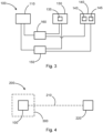
- Fig. 3 shows how the components of the modulator unit 100 are controlled in order to incorporate the information to be transmitted into the polarization of the optical signal.
- the modulator unit 100 includes a power supply 160 and a control unit 150. Both the power supply 160 and the control unit 150 are connected to the light source 110, the EOM 130 and the Faraday mirror 140. However, the control unit 150 can also be connected directly to the power supply 160 in order to specify an electrical voltage output by the power supply 160 at the respective connection.
- the power supply 160 supplies the light source 110 with electrical energy so that the light source generates the optical signal that functions as an input signal.
- the power supply 160 also supplies the EOM 130 electrical energy, for example an electrical voltage, which is applied to a crystal 135. This electrical voltage influences the crystal 135 in such a way that the phase of a portion of a passing optical signal that is polarized in a certain way is changed. For example, variations in electrical voltage can change the phase to different degrees.
- the control unit 150 and the power supply 160 control the EOM so that it acts on the optical signal passing through the EOM in the desired manner on the outward and return path of the optical signal and changes the phase of the influenced polarization component accordingly and as desired.
- the control unit and the energy supply must switch accordingly quickly and control the EOM.
- the polarization of a passing optical signal is changed in the Faraday rotator 143, in the present example by 45°. Then the optical signal hits the mirror 145, is reflected by it and passes through the Faraday rotator 143 again. Now the polarization of the optical signal is changed again by 45 ° in the same direction, so that the polarization of the signals incident on the Faraday mirror changes optical signal and the polarization of the optical signal output by the Faraday mirror differs by 90°.
- the control unit 150 is designed to control the energy supply 160 and/or each of the components 110, 130, 140 in such a way that these components are supplied with the energy required for their function.
- the control unit 150 can send control commands to the components 110, 130, 140 and/or control commands to the power supply 160.
- Fig. 4 shows an optical signal transmission path 200.
- a modulator unit 100 acts as a signal source or transmitter.
- the modulator unit 100 modulates the polarization of an optical signal as described above and sends the modulated optical signal over a transmission path 210.
- the transmission path 210 is, for example, a wireless optical path.
- the modulated optical signal is received and processed by a remote station.
- the remote station is the receiver 220.
- the modulator unit 100 can be arranged on board a satellite.
- the receiver 220 may be located on the Earth's surface or on board another satellite.
Landscapes
- Physics & Mathematics (AREA)
- Electromagnetism (AREA)
- Engineering & Computer Science (AREA)
- Computer Networks & Wireless Communication (AREA)
- Signal Processing (AREA)
- General Physics & Mathematics (AREA)
- Optics & Photonics (AREA)
- Astronomy & Astrophysics (AREA)
- Optical Communication System (AREA)
Applications Claiming Priority (1)
| Application Number | Priority Date | Filing Date | Title |
|---|---|---|---|
| DE102022119077.3A DE102022119077B3 (de) | 2022-07-29 | 2022-07-29 | Modulatoreinheit zum Modulieren der Polarisation eines optischen Signals, optische Signalübertragungsstrecke sowie Satellit |
Publications (2)
| Publication Number | Publication Date |
|---|---|
| EP4322425A1 true EP4322425A1 (fr) | 2024-02-14 |
| EP4322425B1 EP4322425B1 (fr) | 2024-11-27 |
Family
ID=87419222
Family Applications (1)
| Application Number | Title | Priority Date | Filing Date |
|---|---|---|---|
| EP23186293.9A Active EP4322425B1 (fr) | 2022-07-29 | 2023-07-19 | Modulateur de polarisation a autocompensation |
Country Status (4)
| Country | Link |
|---|---|
| US (1) | US20240039633A1 (fr) |
| EP (1) | EP4322425B1 (fr) |
| DE (1) | DE102022119077B3 (fr) |
| ES (1) | ES3017133T3 (fr) |
Families Citing this family (1)
| Publication number | Priority date | Publication date | Assignee | Title |
|---|---|---|---|---|
| DE102022131465B3 (de) * | 2022-11-29 | 2024-02-22 | Tesat-Spacecom Gmbh & Co. Kg | Modulatoreinheit zum Modulieren der Polarisation eines optischen Signals, optische Signalübertragungsstrecke sowie Satellit |
Citations (2)
| Publication number | Priority date | Publication date | Assignee | Title |
|---|---|---|---|---|
| US6333808B1 (en) * | 2000-04-28 | 2001-12-25 | Alcatel | Optical signal scrambling |
| US6459518B1 (en) * | 1998-06-12 | 2002-10-01 | Kdd Corporation | Optical transmitting apparatus |
Family Cites Families (8)
| Publication number | Priority date | Publication date | Assignee | Title |
|---|---|---|---|---|
| JP4738040B2 (ja) * | 2005-03-29 | 2011-08-03 | 富士通株式会社 | 光通信システム、伝送劣化補償方法 |
| US8396373B2 (en) * | 2008-03-27 | 2013-03-12 | Cubic Corporation | Modulating retro-reflector optical communication using polarization differential signaling |
| US9128242B2 (en) * | 2011-12-15 | 2015-09-08 | Mitsubishi Electric Research Laboratories, Inc. | Mode-evolution compound converter |
| US9647426B1 (en) * | 2013-06-28 | 2017-05-09 | Aurrion, Inc. | Polarization insensitive colorless optical devices |
| US10411430B1 (en) * | 2015-04-20 | 2019-09-10 | Aurrion, Inc. | Optical system and method for locking a wavelength of a tunable laser |
| US10330959B2 (en) * | 2017-05-22 | 2019-06-25 | Futurewei Technologies, Inc. | Polarization insensitive micro ring modulator |
| US11770190B1 (en) * | 2022-06-24 | 2023-09-26 | Rockwell Collins, Inc. | Multiple-sensitivity optical phase modulator |
| CN118300695A (zh) * | 2024-03-29 | 2024-07-05 | 济南量子技术研究院 | 基于扰动的qkd时间相关性光源侧信道抑制方法及其发送端 |
-
2022
- 2022-07-29 DE DE102022119077.3A patent/DE102022119077B3/de active Active
-
2023
- 2023-07-19 EP EP23186293.9A patent/EP4322425B1/fr active Active
- 2023-07-19 ES ES23186293T patent/ES3017133T3/es active Active
- 2023-07-28 US US18/227,509 patent/US20240039633A1/en active Pending
Patent Citations (2)
| Publication number | Priority date | Publication date | Assignee | Title |
|---|---|---|---|---|
| US6459518B1 (en) * | 1998-06-12 | 2002-10-01 | Kdd Corporation | Optical transmitting apparatus |
| US6333808B1 (en) * | 2000-04-28 | 2001-12-25 | Alcatel | Optical signal scrambling |
Also Published As
| Publication number | Publication date |
|---|---|
| EP4322425B1 (fr) | 2024-11-27 |
| US20240039633A1 (en) | 2024-02-01 |
| ES3017133T3 (en) | 2025-05-12 |
| DE102022119077B3 (de) | 2023-10-05 |
Similar Documents
| Publication | Publication Date | Title |
|---|---|---|
| DE69526019T2 (de) | Synchrone Polarisations-und-Phasenmodulation zur verbesserten Leistung eines optischen Übertragungssystems | |
| DE69331167T2 (de) | Optischer Impulsgeber | |
| DE69221121T2 (de) | Programmierbare faseroptische verzögerungsleitung, und damit ausgestattetes radarzielsimulationssystem | |
| DE69633816T2 (de) | Synchrone Polarisations- und Phasenmodulation mit einer periodischen Wellenform mit harmonischen Oberschwingungen zur Leistungsverbesserung von optischen Übertragungssystemen | |
| DE69725360T2 (de) | Verfahren zur optischen Übertragung von digitalen Daten | |
| EP0461380B1 (fr) | Système de transmission de données radio, notamment système de radio mobile cellulaire | |
| DE69915553T2 (de) | Verfahren zur Kompensation der Polarisationsmodendispersion | |
| DE69332131T2 (de) | Optischer Modulator, optischer Sender und optisches Übertragungssystem | |
| EP0354567B1 (fr) | Ensemble émission-réception pour un système de communication bidirectionnel cohérent et optique | |
| DE10208712A1 (de) | Phasengesteuerte Antennengruppe mit einer verstärkungsgeschalteten Multi-Mode-Fabry-Perot-Laserdiode und einer Faser hoher Dispersion | |
| DE69632733T2 (de) | Dispersionskompensation | |
| DE102017127813A1 (de) | Strahlausrichtung in unidirektionalen optischen Kommunikationssystemen | |
| EP4322425B1 (fr) | Modulateur de polarisation a autocompensation | |
| DE3637809A1 (de) | Sender fuer kohaerente lichtwellen | |
| DE19856586A1 (de) | Optischer Modulator mit einem Isolator und optischer Sender, der diesen umfaßt | |
| DE69801709T2 (de) | Optisches Übertragungssystem mit dynamischer Kompensation der übertragenen Leistung | |
| EP0883253B1 (fr) | Procédé et dispositif d'optimisation de connexions optiques entre satellites | |
| EP3011648B1 (fr) | Oscillateur optoélectronique | |
| DE3641541C1 (de) | Leitstrahl-Einrichtung fuer ein Flugkoerperlenksystem | |
| DE69017359T2 (de) | Verfahren und Vorrichtung zur Übertragung eines elektromagnetischen Signals in einer optischen Faser. | |
| DE102022131465B3 (de) | Modulatoreinheit zum Modulieren der Polarisation eines optischen Signals, optische Signalübertragungsstrecke sowie Satellit | |
| EP4328660B1 (fr) | Modulateur de polarisation à autocompensation utilisant un déphaseur directionnel | |
| DE69129977T2 (de) | Optischer Sender | |
| EP0612451B1 (fr) | Dispositif pour produire des signaux de retroaction pour la regulation de circuits de surveillance optiques (pll) | |
| EP4593325A1 (fr) | Dispositif de génération d'au moins une clé quantique utilisant un codage de temps-bin et/ou de polarisation et procédé de génération d'au moins une clé quantique |
Legal Events
| Date | Code | Title | Description |
|---|---|---|---|
| PUAI | Public reference made under article 153(3) epc to a published international application that has entered the european phase |
Free format text: ORIGINAL CODE: 0009012 |
|
| STAA | Information on the status of an ep patent application or granted ep patent |
Free format text: STATUS: THE APPLICATION HAS BEEN PUBLISHED |
|
| STAA | Information on the status of an ep patent application or granted ep patent |
Free format text: STATUS: REQUEST FOR EXAMINATION WAS MADE |
|
| AK | Designated contracting states |
Kind code of ref document: A1 Designated state(s): AL AT BE BG CH CY CZ DE DK EE ES FI FR GB GR HR HU IE IS IT LI LT LU LV MC ME MK MT NL NO PL PT RO RS SE SI SK SM TR |
|
| 17P | Request for examination filed |
Effective date: 20240122 |
|
| RBV | Designated contracting states (corrected) |
Designated state(s): AL AT BE BG CH CY CZ DE DK EE ES FI FR GB GR HR HU IE IS IT LI LT LU LV MC ME MK MT NL NO PL PT RO RS SE SI SK SM TR |
|
| GRAP | Despatch of communication of intention to grant a patent |
Free format text: ORIGINAL CODE: EPIDOSNIGR1 |
|
| STAA | Information on the status of an ep patent application or granted ep patent |
Free format text: STATUS: GRANT OF PATENT IS INTENDED |
|
| RIC1 | Information provided on ipc code assigned before grant |
Ipc: H04B 10/00 20130101AFI20240624BHEP |
|
| INTG | Intention to grant announced |
Effective date: 20240716 |
|
| GRAS | Grant fee paid |
Free format text: ORIGINAL CODE: EPIDOSNIGR3 |
|
| GRAA | (expected) grant |
Free format text: ORIGINAL CODE: 0009210 |
|
| STAA | Information on the status of an ep patent application or granted ep patent |
Free format text: STATUS: THE PATENT HAS BEEN GRANTED |
|
| AK | Designated contracting states |
Kind code of ref document: B1 Designated state(s): AL AT BE BG CH CY CZ DE DK EE ES FI FR GB GR HR HU IE IS IT LI LT LU LV MC ME MK MT NL NO PL PT RO RS SE SI SK SM TR |
|
| REG | Reference to a national code |
Ref country code: GB Ref legal event code: FG4D Free format text: NOT ENGLISH |
|
| REG | Reference to a national code |
Ref country code: CH Ref legal event code: EP |
|
| REG | Reference to a national code |
Ref country code: IE Ref legal event code: FG4D Free format text: LANGUAGE OF EP DOCUMENT: GERMAN |
|
| REG | Reference to a national code |
Ref country code: DE Ref legal event code: R096 Ref document number: 502023000335 Country of ref document: DE |
|
| REG | Reference to a national code |
Ref country code: LT Ref legal event code: MG9D |
|
| REG | Reference to a national code |
Ref country code: NL Ref legal event code: MP Effective date: 20241127 |
|
| PG25 | Lapsed in a contracting state [announced via postgrant information from national office to epo] |
Ref country code: IS Free format text: LAPSE BECAUSE OF FAILURE TO SUBMIT A TRANSLATION OF THE DESCRIPTION OR TO PAY THE FEE WITHIN THE PRESCRIBED TIME-LIMIT Effective date: 20250327 Ref country code: PT Free format text: LAPSE BECAUSE OF FAILURE TO SUBMIT A TRANSLATION OF THE DESCRIPTION OR TO PAY THE FEE WITHIN THE PRESCRIBED TIME-LIMIT Effective date: 20250327 Ref country code: HR Free format text: LAPSE BECAUSE OF FAILURE TO SUBMIT A TRANSLATION OF THE DESCRIPTION OR TO PAY THE FEE WITHIN THE PRESCRIBED TIME-LIMIT Effective date: 20241127 |
|
| PG25 | Lapsed in a contracting state [announced via postgrant information from national office to epo] |
Ref country code: FI Free format text: LAPSE BECAUSE OF FAILURE TO SUBMIT A TRANSLATION OF THE DESCRIPTION OR TO PAY THE FEE WITHIN THE PRESCRIBED TIME-LIMIT Effective date: 20241127 Ref country code: NL Free format text: LAPSE BECAUSE OF FAILURE TO SUBMIT A TRANSLATION OF THE DESCRIPTION OR TO PAY THE FEE WITHIN THE PRESCRIBED TIME-LIMIT Effective date: 20241127 |
|
| PG25 | Lapsed in a contracting state [announced via postgrant information from national office to epo] |
Ref country code: BG Free format text: LAPSE BECAUSE OF FAILURE TO SUBMIT A TRANSLATION OF THE DESCRIPTION OR TO PAY THE FEE WITHIN THE PRESCRIBED TIME-LIMIT Effective date: 20241127 |
|
| PG25 | Lapsed in a contracting state [announced via postgrant information from national office to epo] |
Ref country code: NO Free format text: LAPSE BECAUSE OF FAILURE TO SUBMIT A TRANSLATION OF THE DESCRIPTION OR TO PAY THE FEE WITHIN THE PRESCRIBED TIME-LIMIT Effective date: 20250227 |
|
| PG25 | Lapsed in a contracting state [announced via postgrant information from national office to epo] |
Ref country code: LV Free format text: LAPSE BECAUSE OF FAILURE TO SUBMIT A TRANSLATION OF THE DESCRIPTION OR TO PAY THE FEE WITHIN THE PRESCRIBED TIME-LIMIT Effective date: 20241127 |
|
| PG25 | Lapsed in a contracting state [announced via postgrant information from national office to epo] |
Ref country code: PL Free format text: LAPSE BECAUSE OF FAILURE TO SUBMIT A TRANSLATION OF THE DESCRIPTION OR TO PAY THE FEE WITHIN THE PRESCRIBED TIME-LIMIT Effective date: 20241127 |
|
| PG25 | Lapsed in a contracting state [announced via postgrant information from national office to epo] |
Ref country code: RS Free format text: LAPSE BECAUSE OF FAILURE TO SUBMIT A TRANSLATION OF THE DESCRIPTION OR TO PAY THE FEE WITHIN THE PRESCRIBED TIME-LIMIT Effective date: 20250227 |
|
| REG | Reference to a national code |
Ref country code: ES Ref legal event code: FG2A Ref document number: 3017133 Country of ref document: ES Kind code of ref document: T3 Effective date: 20250512 |
|
| PG25 | Lapsed in a contracting state [announced via postgrant information from national office to epo] |
Ref country code: SM Free format text: LAPSE BECAUSE OF FAILURE TO SUBMIT A TRANSLATION OF THE DESCRIPTION OR TO PAY THE FEE WITHIN THE PRESCRIBED TIME-LIMIT Effective date: 20241127 |
|
| PG25 | Lapsed in a contracting state [announced via postgrant information from national office to epo] |
Ref country code: DK Free format text: LAPSE BECAUSE OF FAILURE TO SUBMIT A TRANSLATION OF THE DESCRIPTION OR TO PAY THE FEE WITHIN THE PRESCRIBED TIME-LIMIT Effective date: 20241127 |
|
| PG25 | Lapsed in a contracting state [announced via postgrant information from national office to epo] |
Ref country code: EE Free format text: LAPSE BECAUSE OF FAILURE TO SUBMIT A TRANSLATION OF THE DESCRIPTION OR TO PAY THE FEE WITHIN THE PRESCRIBED TIME-LIMIT Effective date: 20241127 |
|
| PG25 | Lapsed in a contracting state [announced via postgrant information from national office to epo] |
Ref country code: RO Free format text: LAPSE BECAUSE OF FAILURE TO SUBMIT A TRANSLATION OF THE DESCRIPTION OR TO PAY THE FEE WITHIN THE PRESCRIBED TIME-LIMIT Effective date: 20241127 |
|
| PG25 | Lapsed in a contracting state [announced via postgrant information from national office to epo] |
Ref country code: SK Free format text: LAPSE BECAUSE OF FAILURE TO SUBMIT A TRANSLATION OF THE DESCRIPTION OR TO PAY THE FEE WITHIN THE PRESCRIBED TIME-LIMIT Effective date: 20241127 |
|
| PG25 | Lapsed in a contracting state [announced via postgrant information from national office to epo] |
Ref country code: CZ Free format text: LAPSE BECAUSE OF FAILURE TO SUBMIT A TRANSLATION OF THE DESCRIPTION OR TO PAY THE FEE WITHIN THE PRESCRIBED TIME-LIMIT Effective date: 20241127 |
|
| REG | Reference to a national code |
Ref country code: DE Ref legal event code: R097 Ref document number: 502023000335 Country of ref document: DE |
|
| PG25 | Lapsed in a contracting state [announced via postgrant information from national office to epo] |
Ref country code: SE Free format text: LAPSE BECAUSE OF FAILURE TO SUBMIT A TRANSLATION OF THE DESCRIPTION OR TO PAY THE FEE WITHIN THE PRESCRIBED TIME-LIMIT Effective date: 20241127 |
|
| PLBE | No opposition filed within time limit |
Free format text: ORIGINAL CODE: 0009261 |
|
| STAA | Information on the status of an ep patent application or granted ep patent |
Free format text: STATUS: NO OPPOSITION FILED WITHIN TIME LIMIT |
|
| PGFP | Annual fee paid to national office [announced via postgrant information from national office to epo] |
Ref country code: ES Payment date: 20250828 Year of fee payment: 3 |
|
| PGFP | Annual fee paid to national office [announced via postgrant information from national office to epo] |
Ref country code: DE Payment date: 20250722 Year of fee payment: 3 |
|
| PGFP | Annual fee paid to national office [announced via postgrant information from national office to epo] |
Ref country code: IT Payment date: 20250731 Year of fee payment: 3 |
|
| PGFP | Annual fee paid to national office [announced via postgrant information from national office to epo] |
Ref country code: FR Payment date: 20250725 Year of fee payment: 3 Ref country code: AT Payment date: 20251020 Year of fee payment: 3 |
|
| 26N | No opposition filed |
Effective date: 20250828 |
|
| PG25 | Lapsed in a contracting state [announced via postgrant information from national office to epo] |
Ref country code: LU Free format text: LAPSE BECAUSE OF NON-PAYMENT OF DUE FEES Effective date: 20250719 |
|
| REG | Reference to a national code |
Ref country code: BE Ref legal event code: MM Effective date: 20250731 |
|
| PG25 | Lapsed in a contracting state [announced via postgrant information from national office to epo] |
Ref country code: BE Free format text: LAPSE BECAUSE OF NON-PAYMENT OF DUE FEES Effective date: 20250731 |