EP4382875B1 - Dehnungsmessstreifen - Google Patents
Dehnungsmessstreifen Download PDFInfo
- Publication number
- EP4382875B1 EP4382875B1 EP23212689.6A EP23212689A EP4382875B1 EP 4382875 B1 EP4382875 B1 EP 4382875B1 EP 23212689 A EP23212689 A EP 23212689A EP 4382875 B1 EP4382875 B1 EP 4382875B1
- Authority
- EP
- European Patent Office
- Prior art keywords
- layer
- resonator
- substrate
- pad
- fixed
- Prior art date
- Legal status (The legal status is an assumption and is not a legal conclusion. Google has not performed a legal analysis and makes no representation as to the accuracy of the status listed.)
- Active
Links
Images


Classifications
-
- G—PHYSICS
- G01—MEASURING; TESTING
- G01L—MEASURING FORCE, STRESS, TORQUE, WORK, MECHANICAL POWER, MECHANICAL EFFICIENCY, OR FLUID PRESSURE
- G01L1/00—Measuring force or stress, in general
- G01L1/24—Measuring force or stress, in general by measuring variations of optical properties of material when it is stressed, e.g. by photoelastic stress analysis using infrared, visible light, ultraviolet
-
- G—PHYSICS
- G01—MEASURING; TESTING
- G01D—MEASURING NOT SPECIALLY ADAPTED FOR A SPECIFIC VARIABLE; ARRANGEMENTS FOR MEASURING TWO OR MORE VARIABLES NOT COVERED IN A SINGLE OTHER SUBCLASS; TARIFF METERING APPARATUS; MEASURING OR TESTING NOT OTHERWISE PROVIDED FOR
- G01D5/00—Mechanical means for transferring the output of a sensing member; Means for converting the output of a sensing member to another variable where the form or nature of the sensing member does not constrain the means for converting; Transducers not specially adapted for a specific variable
- G01D5/26—Mechanical means for transferring the output of a sensing member; Means for converting the output of a sensing member to another variable where the form or nature of the sensing member does not constrain the means for converting; Transducers not specially adapted for a specific variable characterised by optical transfer means, i.e. using infrared, visible, or ultraviolet light
- G01D5/268—Mechanical means for transferring the output of a sensing member; Means for converting the output of a sensing member to another variable where the form or nature of the sensing member does not constrain the means for converting; Transducers not specially adapted for a specific variable characterised by optical transfer means, i.e. using infrared, visible, or ultraviolet light using optical fibres
Definitions
- This description relates generally to integrated circuits, and more particularly to integrated circuits implementing a strain gauge.
- Known integrated circuits include a piezoresistive or photonic strain gauge for measuring a strain of an element, the strain gauge being attached to and in contact with the element whose strain is being measured such that a strain of that element causes a corresponding strain of the strain gauge.
- Known photonic integrated circuits propose to measure a displacement between a first element and a second element movable relative to each other.
- These circuits comprise an opto-mechanical strain gauge comprising an optical resonator fixed to the first element, such that a displacement of the two elements relative to each other causes a variation (or deformation) of a mechanical gap between the optical resonator and the second element, or a variation (or deformation) of an optical gap between the resonator and a waveguide fixed to the second element.
- the variation of the mechanical gap causes a change in the effective optical index of the resonator resulting from the change in the gap separating the first and second elements, and therefore a corresponding and measurable change in its resonance wavelength.
- the variation of the optical gap where the waveguide is optically coupled to the optical resonator, causes a corresponding and measurable change in the optical coupling between the waveguide and the resonator.
- known optomechanical strain gauges make it possible to do without the electrical connections required for the polarization and measurement of the strain of the piezoresistive gauge.
- One embodiment overcomes all or part of the drawbacks of known devices comprising an opto-mechanical strain gauge known for measuring a relative displacement between two elements movable relative to each other.
- the first and second anchoring pads are arranged inside the resonator.
- the first and second portions of the resonator each have a semi-circular shape.
- each of the first and second beams has a larger cross-section on the side of its second end than on the side of its first end.
- the resonator comprises a third portion connecting the first portion of the resonator to the second portion of the resonator, and another third portion connecting the second portion of the resonator to the first portion of the resonator, the set of the first, second and third portions forming the ring of the resonator.
- each of the first and second portions of the resonator has a cross-section configured to allow multimode guiding of light
- each of the third portions has a central portion having a cross-section configured to allow single-mode guiding of light.
- the first and second parts of the first layer are movable relative to each other in a first direction parallel to the substrate.
- the second layer is disposed between the substrate and the first layer, the first and second portions of the first layer being suspended above the substrate.
- the device further comprises a waveguide defined in the second layer and having a portion optically coupled to the resonator, said portion of the waveguide being either optically coupled to the first portion of the resonator and attached to the first portion of the first layer, or optically coupled to the second portion of the resonator and attached to the second portion of the first layer.
- the expressions “approximately”, “approximately”, “substantially”, and “of the order of” mean to within 10%, preferably to within 5%.
- a device comprising a substrate, a first layer indirectly resting on the substrate and a ring optical resonator defined in a second layer, wherein the first layer comprises a first portion and a second portion configured to be movable relative to each other, for example in a direction parallel to the substrate, and wherein the resonator has a first portion attached to the first portion of the first layer and a second portion attached to the second portion of the second layer.
- portions of the resonator that connect the first and second portions of the resonator to form the resonator ring deform, for example compress or expand in the aforementioned direction.
- These deformations of the ring cause a corresponding change in its resonance wavelength.
- FIG 1 represents, by a schematic top view, an example of an embodiment of such a device 1.
- the figure 2 is a schematic sectional view of the device 1 taken in the plane AA of the figure 1
- there figure 3 being a schematic sectional view of the device 1 taken in the plane BB of the figure 1
- there figure 4 being a schematic sectional view of the device 1 taken in the plane CC of the figure 1
- the figure 5 being a schematic sectional view of the device 1 taken in the plane DD of the figure 1 .
- the device 1 comprises a substrate 100, for example a semiconductor substrate.
- the circuit 1 is formed on the substrate 100.
- the substrate 100 has a thickness of several hundred micrometers, for example a thickness of at least 200 ⁇ m.
- the substrate 100 may have been thinned and have a thickness of less than 200 ⁇ m.
- the device 1 further comprises a layer 102.
- the thickness of the layer 102 is less than 100 ⁇ m, for example less than 10 ⁇ m, or even less than 1 ⁇ m.
- the layer 102 comprises a portion 102A and a portion 102B.
- each of the two portions 102A and 102B is suspended above the substrate 100, i.e., a free space is provided between the substrate 100 and each of these portions 102A and 102B.
- the portions 102A and 102B are movable relative to each other, preferably in a direction parallel to the substrate 100. In the example of Figures 1 to 5 , the two parts 102A and 102B are movable relative to each other in a direction X, parallel to the substrate 100.
- one of the portions 102A and 102B is fixed relative to the substrate and the other of the portions 102A and 102B is movable relative to the substrate 100, such that the portions 102A and 102B are movable relative to each other.
- both of the portions 102A and 102B are movable relative to the substrate 100, such that both of the portions 102A and 102B are movable relative to each other.
- this portion of the layer 102 is mechanically connected to another portion of the layer 102 which is fixed to the substrate by a stack of layers in contact two by two, this stack being connected on the one hand to the substrate and on the other hand to this other part of the layer 102.
- each deformable connection corresponds to, or comprises, a portion of layer 102.
- each deformable connection corresponds to, or comprises, a portion of a layer other than the layer 102, the layer 102 resting on this other layer or this other layer resting on the layer 102.
- the part 102A is fixed relative to the substrate 100 and the part 102B is movable relative to the substrate 100, and therefore relative to the part 102A, for example in the X direction.
- portion 102A of layer 102 is mechanically connected to portion 102C of layer 102, portion 102C being attached to substrate 100 by a stack 104 of layers.
- Stack 104 is mechanically connected to substrate 100 and portion 102C of layer 102.
- figures 1, 2, 3 And 5 the boundary between part 102A and part 102C of layer 102 is represented by a dotted line.
- portion 102B of layer 102 is coupled to portion 102D of layer 102, with portion 102D being attached to substrate 100 by a stack 106 of layers.
- the stack 106 is, for example, identical to the stack 104 except that the stack 106 is mechanically connected to the substrate 100 and to the portion 102D of the layer 102 instead of being mechanically connected to the substrate 100 and to the portion 102C of the layer 102.
- the portions 102B and 102D of the layer 102 are mechanically coupled to each other by deformable links 108, for example links 108 deformable in the X direction.
- the links 108 comprise, for example, each a portion of the layer 102.
- each link 108 is a corresponding portion of the layer 102.
- each link 108 corresponds to a beam, for example defined in layer 102, each beam having one end connected to part 102D of layer 102 and another end connected to part 102B of layer 102.
- each link 108 corresponds to one or more meanders, for example defined in layer 102. The person skilled in the art will be able to provide other shapes for the links 108.
- the device 1 further comprises an annular optical resonator 110.
- the resonator has the shape of an athletics track ("racetrack” in English), that is to say a ring comprising two semi-circular parts connected to each other by two rectilinear parts.
- the resonator 110 is formed in, or defined in, a layer 112. In other words, the resonator 110 is implemented by a portion of layer 112.
- Layer 112 is made of a material suitable for guiding light at the operating wavelengths of circuit 1.
- layer 112 is made of silicon, silicon nitride, arsenic gallium or germanium.
- the layer 112 is arranged between the substrate 100 and the layer 102.
- the stack 104 and/or the stack 106 may comprise a portion of the layer 112.
- the elements, in particular the portions of layer 112, arranged under the layer 102 are delimited by dotted lines.
- the layer 112 is arranged above the layer 102, the layer 102 itself being arranged above the substrate 100.
- Layer 112 is separated from layer 102 by a single layer 116.
- the resonator 110 comprises a first portion 110A fixed to the portion 102A of the layer 102, and a second portion 110B fixed to the portion 102B of the layer 102. More precisely, the portion 110A of the resonator 110 is fixed to an anchoring pad 114A which is mechanically connected to the portion 102A of the layer 102, and the portion 110B of the resonator 110 is fixed to an anchoring pad 114B which is mechanically connected to the portion 102B of the layer 102.
- the portion 110A preferably corresponds to one of the two semicircular portions of the ring 110, the portion 110B preferably corresponding to the other of the two semicircular portions of the ring 110.
- the resonator 110 is not fixed to the substrate 100, i.e., it is not fixed to an anchor pad connected to the substrate 100.
- the device 1 comprises only two pads 114A and 114B making it possible to fix the resonator 110 to the layer 102.
- the resonator comprises two portions 110C, for example rectilinear, each connecting the portion 110A to the portion 110B so that all of the portions 110A, 110B and 110C placed end to end form the ring of the resonator 110.
- the portions 110C are rectilinear, they are aligned with the direction X of movement of the parts 102A and 102B relative to each other.
- these portions 110C may not be rectilinear, for example comprise one or more curves, although they are preferably each substantially aligned in the direction of their length with the direction X of movement.
- the portions 110C of the resonator 110 which causes a variation in its resonance wavelength. It is therefore the portions 110C of the resonator 110 which here act as an optomechanical strain gauge.
- the portion 110A, respectively 110B, of the resonator 110 is fixed to the pad 114A, respectively 114B, by one or more portions of the layer 112 each extending from the portion 110A, respectively 110B, to the pad 114A, respectively 114B.
- the anchoring pads 114A, 114B fixing the resonator 110 to the layer 102 are arranged inside the ring 110, that is to say that, when viewed from above, the pads 114A, 114B are arranged in a region laterally delimited by the inner edge of the ring 114.
- each portion of the layer 112 which fixes the resonator 110 to a pad 114A or 114B is in contact with the inner edge of the resonator 110 rather than with the outer edge of the resonator 110, which makes it possible to limit the optical losses in the resonator 110.
- Each pad 114A, 114B comprises, for example, a portion of the layer 112 and a region 115 extending from this portion of the layer 112 to the layer 102.
- the region 115 is mechanically connected to the layer 102 and to the portion of the layer 112 forming part of the pad.
- each region 115 corresponds to a portion of the layer 116.
- each region 115 is made of a material different from that of the layer 116, such that the layer 116 can be selectively etched with respect to this material.
- the layer 112 is separated from the substrate 100 by a single layer 117.
- each stack 104, 106 can then comprise a portion of the layer 116 and a portion of the layer 117 between which a portion of the layer 112 can be arranged.
- the resonator 110 is then suspended under a plane comprising the face of the layer 102 which is facing the substrate 100, and above a plane comprising the face of the substrate 100 which is facing the layer 102. More generally, the resonator 110 is then suspended from the layer 102, between the layer 102 and the substrate.
- resonator 110 is suspended above layer 102.
- this portion of the layer 102 may be fixed to the substrate by a stack 104 of layers in two-by-two contact rather than being first mechanically connected to another portion of the layer 102 which is fixed to the substrate 100 by a stack 104 of layers.
- the portion 102A or 102B of the layer 102 which is fixed relative to the substrate is then not suspended above the substrate 100.
- each pad 114A, 114B is substantially that of a disk.
- the portion 110A respectively 110B, of the resonator 110 is fixed to the pad 114A, respectively 114B, by beams 118A, respectively 118B, defined in the layer 112.
- the portion 110A respectively 110B, of the resonator 110 is fixed to the pad 114A, respectively 114B, by portions 118A, respectively 118B, of the layer 112, each portion 118A, 118B having the shape of a beam.
- Each beam 118A, respectively 118B has one end connected to the portion 110A, respectively 110B, of the resonator 110, and another end connected to the pad 114A, respectively 114B.
- each beam 118A, 118B has a substantially constant cross-section over its entire length. According to an alternative embodiment, each beam 118A, 118B has a smaller cross-section at its end connected to the resonator 110 than at its end connected to the pad.
- the portions 110A, 110B and 110C of the resonator 110 each have a cross-section configured to allow single-mode guiding of the light. in the resonator 110.
- the portions 110A and 110B may have a cross-section configured to allow multimode guiding of the light, and at least a central portion of each of the portions 110C has a cross-section configured to allow single-mode guiding of the light.
- the person skilled in the art is able to provide a gradual transition of the dimensions of the cross-section of the portions 110A and 110B to the dimensions of the cross-section of the central portions of the portions 110C, so as to provide a gradual variation of the effective optical index between these portions.
- the device 1 further comprises a waveguide 120.
- the waveguide 120 is, like the resonator 110, defined in the layer 112, that is to say that it corresponds to, or is constituted by, a portion of the layer 112.
- the waveguide 120 comprises a portion 122 which is optically coupled to the resonator 110.
- portion 122 of waveguide 120 is coupled to portion 110A of resonator 110 and is then attached to portion 102A of layer 102 as illustrated in the example of Figures 1 to 5 .
- portion 122 of waveguide 120 is optically coupled to portion 110B of resonator 110 and is then attached to portion 102B of layer 102. Having portion 122 of waveguide 120 attached to the same portion 102A or 102B as portion 110A or 110B of the resonator to which portion 122 is optically coupled allows the optical coupling gap between waveguide 120 and resonator 110 to be kept constant.
- the portion 122 of the waveguide 120 extends longitudinally in a direction Y parallel to the substrate 100 and orthogonal to the direction X.
- the portion 122 of the waveguide 120 is fixed to this part fixed relative to the substrate, so as to avoid deformations of the waveguide 120 during a relative movement of the parts 102A and 102B relative to each other.
- the portion 122 of the waveguide 120 is fixed to the layer 102 by holding arms 124 and anchoring pads 126.
- the pads 126 are, for example, similar to the pads 114A, 114B, that is to say that they comprise stacks of similar layer portions and are each mechanically connected to the layer 102.
- each pad 126 comprises a portion of the layer 112 and a region 115 corresponding to a portion of the layer 116 or to a material with respect to which the layer 116 can be selectively etched, the region 115 being connected to this portion of the layer 112 and to the layer 102.
- Each holding arm 124 is, for example, a portion of the layer 112 extending from the portion 122 of the waveguide 120 to a corresponding pad 126, that is to say a portion of the layer 112 having one end connected to the portion 122 of the waveguide 120 and one end connected to this pad 126.
- the arms 124 each have the shape of a beam although, in other examples not illustrated, each arm 124 may correspond to several beams placed end to end to form at least one meander or may have still other shapes.
- portion 122 of waveguide 120 is, like resonator 110, suspended from layer 102, between layer 102 and substrate 100.
- waveguide 120 is, like resonator 110, suspended above layer 102.
- the layer 112 initially rests on the layer 117, itself resting on the substrate 100. Then different elements, including the resonator 110, are defined by etching in the layer 112. At this step of etching the layer 112, a portion of the layer 112 can be left in place at the location of each stack 104, 106, so that this stack comprises this portion of the layer 112. Then, the layer 116 is formed on the assembly and then the layer 102 is formed, by deposition or by transfer, on the layer 116.
- each anchor pad 114A, 114B, 126 can be made of the same material as the layer 102 in providing an opening in layer 116 up to layer 112, then filling the opening with the material of layer 102 when depositing this layer 102.
- the region 115 of each anchoring pad 114A, 114B, 126 may be made of a material other than that of layer 102 and that of layer 116 by providing an opening in layer 116 up to layer 112, and filling the opening with this material prior to the formation of the layer 102.
- the region 115 of each anchor pad 114A, 114B, 126 may correspond to a portion of the layer 116.
- portions of the layer 102 are removed during an etching step, then portions of the layers 116 and 117 are removed by selective sacrificial etching relative to the layers 102 and 112 and to the substrate 100 to obtain the circuit 1.
- the etching(s) of the layers 116 and 117 are also selective relative to the material of the regions 115.
- the regions 115 are portions of the layer 116, during the etching of the layer 116, the person of the art is able to provide openings in the layer 102 and/or in the layer 112 so that by controlling the etching time of the layer 116 and/or of the layer 117, the regions 115 are left in place at the end of the etching.
- the region 115 may be slightly set back from the outer edge of the pad.
- the layer 112 when the layer 112 is a semiconductor layer, for example made of silicon, and the layer 117 is an insulating layer, for example made of silicon oxide, the layer 112 can correspond to the semiconductor layer of a semiconductor on insulator (SOI) type structure formed on the substrate 100.
- SOI semiconductor on insulator
- each stack 104, 106 includes a left-in-place portion of layer 117, and may or may not include a left-in-place portion of layer 116. Indeed, it is possible to remove layer 116 from the stack by providing that the layer 102 is formed by deposition, directly in contact with the layer 112 at the location of the stack, the layer 102 then being, for example, planarized.
- the layer 102 corresponds to a portion of a first substrate, for example semiconductor, for example silicon, the layer 116 then resting on this first substrate and the layer 112 then resting on the layer 116.
- elements, including the resonator 110 are formed in the layer 112.
- a filling material, for example identical to the material of the layer 116, is deposited then planarized by stopping before or on the layer 112.
- the substrate 100 coated with the layer 117 is then transferred to the structure before thinning the first substrate so as to leave only the layer 102.
- the following steps for obtaining the circuit 1 are then similar to what was described for the other example above.
- the layer 112 when the layer 112 is a semiconductor layer, for example made of silicon, and the layer 116 is an insulating layer, for example made of silicon oxide, the layer 112 can correspond to the semiconductor layer of a semiconductor on insulator (SOI) type structure formed on the first substrate.
- SOI semiconductor on insulator
- the two ways of manufacturing the circuit 1 that are described above are only examples, and the person skilled in the art is able, from the present description, to provide other methods of manufacturing the circuit 1 using steps that are each customary in the manufacture of photonic circuits.
- the person skilled in the art is able to predict the manufacturing processes for manufacturing the circuit 1 in the case where the layer 112 is arranged above the layer 102.
- the circuit 1 comprises only one layer 116 and one layer 117.
- the layer 116 may correspond to a plurality of layers stacked on top of each other and/or the layer 117 may correspond to a plurality of layers stacked on top of each other.
- the two sacrificial layers 116 and 117 are made of the same material, selectively etchable relative to the material(s) of the layers 102 and 112, of the substrate 100, and, for example, of each region 115.
- the layers 116 and 117 may be made of different materials, each selectively etchable relative to the material(s) of the layers 102 and 112, of the substrate 100, and, for example, of each region 115.
- substrate 100 is made of silicon or arsenic-gallium.
- layer 117 is a layer of silicon oxide or a photonic polymer such as for example BCB (benzocyclobutene).
- BCB benzocyclobutene
- layer 116 is a silicon oxide layer.
- each region 115 is made of silicon, silicon nitride or silicon oxide.
- the person skilled in the art is able to adapt the materials of the layers 116, 112, 117 and 102, of the substrate 100 and, for example, of the regions 115 while retaining the etching selectivities indicated previously.
- the thickness of the layer 112 is between 40 and 1000 nm, for example between 50 and 500 nm.
- the thickness of layer 116 is greater than 500 nm, so that layer 102 does not modify the optical properties of resonator 110.
- the thickness of the layer 117 is greater than 500 nm so that the substrate 100 is sufficiently far from the resonator 110 so as not to modify its optical properties.
- the person skilled in the art is able to adapt the thicknesses of the layers 116, 112, 117 and 102 of the substrate 100.
- Lg is the length of each of the portions 110C
- Ltot is the total length of the resonator 110
- n is the effective optical index in the portions 110C
- ⁇ is the resonance wavelength of the resonator 110.
- the portions 110C deform accordingly, resulting in a variation DLg of the length of each of the portions 110C and a variation Dn of the effective optical index in these portions 110C. This results in a change D ⁇ in the resonance wavelength of the resonator 110.
- D ⁇ / ⁇ A*((DLg/Lg) + (Dn/n)), with A having a form factor equal to 2*Lg/Ltot.
- the device 1 described here makes it possible to obtain dynamic measurement ranges having extents, or widths or amplitudes, greater than those of known strain gauges.
- the dynamic measurement range can be greater than 10 6 , although the bandwidth offered by the optical cavity of the device 1, equal to ⁇ /Q with Q the quality factor of the resonator 110, is higher.
- the device 1 operates in open loop
- the person skilled in the art is able to provide a servocontrol of the wavelength of the light circulating in the waveguide 120 on the wavelength of the resonator 110 when this resonance wavelength varies following a displacement of the two parts 102A and 102B of the layer 102 relative to each other.
- the optical measurement bandwidth is large, e.g. from a few GHz to 100 GHz, although in practice it is limited by the mechanical response of the system.
- a piezoresistive gauge has a much smaller measurement bandwidth and is limited by the product of the gauge resistance and the gauge capacitance (RC product).
- the device 1 has a noise threshold for reading the deformation of the resonator which is very low compared to the noise threshold for reading conventional deformation gauges.
- the portion 122 of the waveguide 120 is fixed to the layer 102.
- the portion 122 of the waveguide could be fixed to the substrate 100 rather than to the layer 102, but in this case the aforementioned advantage of maintaining constant the optical coupling gap between the waveguide 120 and the resonator 110 would be lost, which could distort the measurement.
- FIG. 6 represents, by a partial and schematic top view, an alternative embodiment of a part of the device 1 of the Figures 1 to 5 , and, more particularly, pads 114A, 114B of device 1.
- the portion 110B of the resonator 110, the pad 114B and the arms 118B have been shown, the description of these elements being directly transposable to the portion 110A of the resonator 110, to the pad 114A and to the arms 118A. Only the differences between the embodiment described in relation to the Figures 1 to 5 and the variant embodiment of the figure 6 are described here.
- the stud 114B has, when viewed from above, the shape of a half-disc rather than that of a disc as has been described in relation to the Figures 1 to 5 .
- the center of the half-disc 114B that is to say of a disc which would be formed by the half-disc 114B and another half-disc, is coincident with the center of the portion 110B in an arc of a circle, that is to say the center of a circle which would be formed by the portion 110B in a semicircle and another portion in a semicircle.
- the curved part of the half-disc 114B is turned towards the portion 110B of the resonator, or, more precisely, the entire curved edge of the pad 114B is, in a plane parallel to the substrate 100, opposite the portion 110B of the resonator 110.
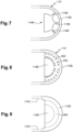
- FIG 7 represents, by a partial and schematic top view, another variant embodiment of a part of the device 1 of the Figures 1 to 5 , and, more particularly, arms 118A, 118B of device 1.
- the portion 110B of the resonator 110, the pad 114B and the arms 118B have been shown, the description of these elements being directly transposable to the portion 110A of the resonator 110, to the pad 114A and to the arms 118A. Only the differences between the embodiment variant described in relation to the figure 6 and the variant embodiment of the figure 7 are described here.
- each beam 118B is beams defined in the layer 112.
- each beam 118B has a larger cross-section on the side of the pad 114B than on the side of the portion 110B of the resonator 110.
- each beam 118B has, on the side of its end connected to the pad 114B, a cross-section which increases as it approaches the pad 114B.
- This embodiment variant applies to cases where the pad 114B has a shape other than that of a half-disc, for example the shape of a disc.
- beams 118B having larger cross-sections on the side of the pad 114B than on the portion 110B of the resonator 110 makes it possible to increase the rigidity of the beams 118B without increasing the optical losses in the resonator 110 compared to the case of beams 118B which would have constant cross-sections over their entire lengths.
- figure 8 represents, by a partial and schematic top view, yet another variant embodiment of a part of the device 1 of the Figures 1 to 5 , and, more particularly, how portions 110A and 110B are fixed to the respective pads 114A and 114B by portions of the layer 112.
- figure 8 only the portion 110B of the resonator 110, the pad 114B and a portion 800 of the layer 112 fixing the portion 110B to the pad 114B have been shown, the description of these elements being directly transposable to the portion 110A of the resonator 110, to the pad 114A and to a portion of the layer 112 fixing the portion 110A to the pad 114A.
- the portion 110B of the resonator 110 is fixed to the pad 114B by arms 118B defined in the layer 112
- the portion 110B of the resonator 110 is fixed to the pad 114B by a portion 800 of the layer 112.
- the portion 800 of the layer 112 fills the space between the pad 114B and the semicircular portion 110B of the resonator 110.
- the portion 800 of the layer 112 is provided with several through openings 802, that is to say openings 802 passing through the layer 112 over its entire thickness. figure 8 , only one opening 802 is referenced so as not to overload the figure.
- the openings 802 are for example configured to implement a photonic crystal structure in the portion 800.
- a portion of the openings 802 implements a photonic crystal structure and another portion of the openings 802 makes it possible to generate high propagation losses on optical modes propagated in the portion 800 and which it is desired to eliminate, i.e. filter.
- the photonic crystal structure is configured so that the light guided in the resonator 110 remains confined in the resonator 110, and, more particularly, in the portion 110B of the resonator 110 when it propagates in this portion 110B.
- the portion 800 and the openings 802 are configured to promote a single optical propagation mode in the portion 110B.
- This embodiment variant applies to cases where the pad 114B has a shape other than that of a half-disc, for example the shape of a disc.
- figure 9 represents, by a partial and schematic top view, yet another variant embodiment of a part of the device 1 of the Figures 1 to 5 , and, more particularly, of the manner in which the portions 110A and 110B are fixed to the respective pads 114A and 114B by portions of the layer 112.
- figure 9 only the portion 110B of the resonator 110, the pad 114B and a portion 900 of the layer 112 fixing the portion 110B to the pad 114B have been shown, the description of these elements being directly transposable to the portion 110A of the resonator 110, to the pad 114A and to a portion of the layer 112 fixing the portion 110A to the pad 114A.
- portion 800 of layer 112 is replaced by a portion 900 of layer 112 identical to the portion 800 except that it does not include the openings 802.
- the propagation of light in the portion 110B is multimode, the portion 110B then having a larger cross-section than that of the central portions 110C of the resonator which is adapted to single-mode propagation.
- a gradual transition from the cross-sectional dimensions of portion 110B to the cross-sectional dimensions of the central portions of portions 110C may be provided, so as to provide a gradual variation in the effective optical index between these portions.
- the manner in which the portion 110A, respectively 110B, of the resonator is fixed to the part 102A, respectively 102B is preferably configured so that the portions 110A and 110B of the resonator do not deform during a relative movement of the parts 102A and 102B relative to each other.
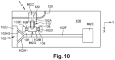
- FIG 10 represents, by a schematic top view, another exemplary embodiment of the device 1.
- the portion 102A of the layer 102 is fixed relative to the substrate 100.
- the layer 102 of the device 1 comprises a portion 102E suspended above the substrate 100.
- the portion 102E has, in a plane parallel to the substrate 100, dimensions greater than those of the portion 102B.
- This portion 102E is movable relative to the substrate 100 in a plane parallel to the substrate 100, for example in a direction identical to the direction X of movement of the portions 102A and 102B relative to each other.
- the layer 102 further comprises a lever arm 102F, 102G.
- the lever arm 102F, 102G is configured such that a movement of the portion 102E in the X-direction results in a corresponding, but smaller, movement of the portion 102B in the X-direction.
- the lever arm 102F, 102G is also suspended above the substrate 100.
- the arm 102F, 102G is defined in the layer 102.
- all or part of the lever arm 102F, 102G may be defined in another of the layers of the device 1.
- the lever arm 102F, 102G here comprises a beam 102F.
- the beam 102F is defined in the layer 102.
- the beam 102F extends lengthwise in the Y direction.
- the beam 102F has one end mechanically connected to the portion 102E, and another end fixed relative to the substrate 100.
- the lever arm 102F, 102G further comprises an element 102G.
- the element 102G is, in this example, defined in the layer 102.
- the layer portion 102G has, for example, a beam shape aligned in the X direction.
- the beam 102G is suspended above the substrate 100.
- the beam 102G is mechanically connected to the portion 102B and to the arm 102F on the fixed end side of the arm 102F.
- the portion 102G of the layer 102 is configured to transmit the movements of the arm 102F in the X direction to the portion 102B of the layer 102.
- the stiffness of the portion 102G in the X direction is at least five times greater than the stiffness of the portions 110C of the resonator 110 in the X direction.
- the beam 102F constitutes an axis whose end which is fixed to the part 102 can move in rotation, in a plane parallel to the substrate 100, around the end of the axis which is fixed relative to the substrate.
- This rotation of the end of the axis 102F which is fixed to the part 102E that is to say the rotation of the part 102E relative to the fixed end of the axis 102F, is considered locally as a translation of the part 102E in the direction X relative to the substrate 100.
- This rotational movement is transmitted in the form of a translational movement in the direction X to that of the parts 102A and 102B which is movable relative to the substrate 100, by means of the element 102G.
- the lever arm is configured to transform a rotational movement, in a plane parallel to the substrate, of the part 102E around the fixed end of the axis 102F into a translational movement, still in a plane parallel to the substrate, of the part 102B.
- the lever arm 102F, 102G By means of the lever arm 102F, 102G there is a linear relationship connecting a displacement of the portion 102E in the X direction and a corresponding smaller displacement of the portion 102B in the X direction.
- the lever arm 102F, 102G allows the displacements of the portion 102B in the X direction to remain within a range where the material of the portions 110C of the resonator 110 is in an elastic deformation regime, while allowing the measurement of displacements of the portion 102E in the X direction and relative to the substrate 100 that are much larger than those of the portion 102B in the X direction and relative to the substrate 100.
- the lever arm 102F, 102G allows the displacements of the portion 102B in the X direction to remain within a range where the material of the portions 110C of the resonator 110 is in an elastic deformation regime, while allowing the measurement of displacements of the portion 102E in the X direction and relative to the substrate 100 that are much larger than those of the portion 102B in the X direction and relative to the substrate 100.
- a displacement of part 102E in the X direction causes a displacement of part 102B in the direction which is Lb/Lp times smaller.
- the fixed end of the axis or beam 102F is connected to the ends of two beams 102H1 and 102H2, for example defined in the layer 102, and forming, in a plane parallel to the substrate 100, a right angle between them at the fixed end of the arm 102F.
- the other ends of the beams 102H1 and 102H2 are mechanically connected to a portion 102J of the layer 102 which is fixed relative to the substrate.
- the two beams 102H1 and 102H2 implement a pivot connection on the fixed end of the arm 102F.
- the torsional stiffness of the portion 102G of the layer 102 is preferably less than that of the pivot connection.
- lever arm 102F allows movement of the portion 102E in the X direction to cause a correspondingly smaller movement of the portion 102B in the X direction
- the lever arm 102F allows movement of the portion 102E in the X direction to cause a correspondingly larger movement of the portion 102B in the X direction.
- lever arm configurations allowing a movement, in a plane parallel to the substrate 100, of the portion 102E relative to the substrate 100 causes, by means of the lever arm, a corresponding movement in this plane of the portions 102A and 102B relative to each other.
- a lever arm designates, in the present description, a system making it possible to convert a rotational movement of the part 102E into a translational movement, preferably in the X direction, of that of the parts 102A and 102B which is movable relative to the substrate 100.
- An example has been described above in the case where a movement of the part 102E in a plane parallel to the substrate 100 is transmitted by the lever arm 102F to one of the parts 102A and 102B (the part 102B in figure 10 ) so as to result in a corresponding movement of the portions 102A and 102B relative to each other in the plane.
- a device 1 comprising a lever arm configured so that a rotational movement of a portion 102E of the layer 102 about an axis parallel to the substrate 100 is transmitted in the form of a translational movement corresponding to that of the portions 102A and 102B which is movable relative to the substrate 100.
- the movement of the portion 102E does not take place in a plane parallel to the substrate 100 as is the case in figure 10 , but at least partly in a direction orthogonal to the substrate 100.
- the portion 102E can then move relative to the substrate 100 in a rotational movement about the axis 102F which is fixed and parallel to the substrate 100.
- This rotational movement about an axis parallel to the substrate 100, and, more particularly parallel to the Y axis in this example, is then transmitted by the element 102G in the form of a corresponding translational movement, in a plane parallel to the substrate, of the portion 102A or 102B which is movable relative to the substrate 100, for example a translational movement in the X direction.
- the element 102G corresponds for example to a portion of the layer 112, for example in the form of a beam aligned in the X direction, having one end fixed to the part 102A or 102B which is movable relative to the substrate 100, and another end fixed to the part 102E.
- the pads and resonator may be as illustrated in figure 8 with respect to the pad 114B and the portion 110B of the resonator 110, and as illustrated in figure 1 with respect to the pad 114A and the portion 110A of the resonator 110.
Landscapes
- Physics & Mathematics (AREA)
- General Physics & Mathematics (AREA)
- Optical Integrated Circuits (AREA)
- Laser Beam Processing (AREA)
Claims (15)
- Vorrichtung (1), die Folgendes aufweist:ein Substrat (100);eine erste Schicht (102), die auf dem Substrat aufliegt, wobei die erste Schicht einen ersten Teil (102A) und einen zweiten Teil (102B) aufweist, die in zueinander beweglich sind;einen ringförmigen optischen Resonator (110), der in einer zweiten Schicht (112) definiert ist, wobei die Vorrichtung dadurch gekennzeichnet ist, dass der Resonator (110) einen ersten Abschnitt (110A), der an einem ersten Ankerkontakt (114A) befestigt ist, der mit dem ersten Teil (102A) der ersten Schicht (102) verbunden ist, und einen zweiten Abschnitt (110B) aufweist, der an einem zweiten Ankerkontakt (114B) befestigt ist, der mit dem zweiten Teil (102B) der ersten Schicht (102) verbunden ist.
- Vorrichtung nach Anspruch 1, wobei die ersten und zweiten Ankerkontakte (114A, 114B) innerhalb des Resonators (110) angeordnet sind.
- Vorrichtung nach Anspruch 1 oder 2, wobei die ersten und zweiten Abschnitte (110A, 110B) des Resonators (110) jeweils eine Halbkreisform aufweisen.
- Vorrichtung nach Anspruch 3 in Abhängigkeit von Anspruch 2, wobei:der erste Ankerkontakt (114A) die Form einer Halbscheibe hat, deren Mittelpunkt mit dem Mittelpunkt des ersten Abschnitts (110A) des Resonators (110) zusammenfällt und deren gekrümmter Abschnitt dem ersten Abschnitt (110A) des Resonators (110) zugewandt ist; und/oderder zweite Kontakt (114B) die Form einer Halbscheibe hat, deren Mitte mit der Mitte des zweiten Abschnitts (110B) des Resonators (110) zusammenfällt und deren gekrümmter Abschnitt dem zweiten Abschnitt (110B) des Resonators (110) zugewandt ist.
- Vorrichtung nach einem der Ansprüche 1 bis 4, wobei:der erste Abschnitt (110A) des Resonators an dem ersten Kontakt (114A) durch erste Träger (118A) befestigt ist, die in der zweiten Schicht (112) definiert sind, wobei jeder der ersten Träger (118A) ein erstes Ende aufweist, das mit dem Resonator (110) verbunden ist, und ein zweites Ende, das mit dem ersten Kontakt (114A) verbunden ist; und/oderder zweite Abschnitt (110B) des Resonators an dem zweiten Kontakt (114B) durch zweite Träger (118B) befestigt ist, die in der zweiten Schicht (112) definiert sind, wobei jeder der zweiten Träger (118B) ein erstes Ende aufweist, das mit dem Resonator (110) verbunden ist, und ein zweites Ende, das mit dem zweiten Kontakt (114B) verbunden ist.
- Vorrichtung nach Anspruch 5, wobei jeder der ersten und zweiten Träger (118A, 118B) auf der Seite seines zweiten Endes eine größere Querschnittsfläche aufweist als auf der Seite seines ersten Endes.
- Vorrichtung nach einem der Ansprüche 1 bis 4, wobei:der erste Abschnitt (110A) des Resonators an dem ersten Kontakt (114A) durch einen ersten durchgehenden Abschnitt (900) der zweiten Schicht (112) befestigt ist, wobei die Anordnung aus erstem Abschnitts (110A) des Resonators, erstem Abschnitt (900) der zweiten Schicht (112) und erstem Kontakt (114A) eine Form einer Halbscheibe aufweist; und/oderder zweite Abschnitt (110B) des Resonators an dem zweiten Kontakt (114B) durch einen zweiten durchgehenden Abschnitt (900) der zweiten Schicht (112) befestigt ist, wobei die Anordnung aus zweitem Abschnitt (110B) des Resonators (110), zweitem Abschnitt (900) der zweiten Schicht (112) und zweitem Kontakt (114B) eine Form einer Halbscheibe aufweist.
- Vorrichtung nach einem der Ansprüche 1 bis 4, wobei:der erste Abschnitt (110A) des Resonators an dem ersten Kontakt (114A) durch einen ersten Abschnitt (800) der zweiten Schicht (112) befestigt ist, wobei die Anordnung aus erstem Abschnitt (110A) des Resonators, erstem Abschnitt (800) der zweiten Schicht (112) ) und erstem Kontakt (114A) eine Form einer Halbscheibe aufweist und der erste Abschnitt (800) der zweiten Schicht (112) Durchgangsöffnungen (802) aufweist, die so konfiguriert sind, dass sie einen einzelnen optischen Ausbreitungsmodus in dem ersten Abschnitt (110B) des Resonators (110) begünstigen; und/oderder zweite Abschnitt (110B) des Resonators an dem zweiten Kontakt (114B) durch einen zweiten Abschnitt (800) der zweiten Schicht (112) befestigt ist, wobei die Anordnung aus zweitem Abschnitt (110B) des Resonators (110), zweitem Abschnitt (800) der zweiten Schicht ( 112) und zweitem Kontakt (114B) eine Form einer Halbscheibe aufweist und der zweite Abschnitt (800) der zweiten Schicht (112) Durchgangsöffnungen (802) aufweist, die so konfiguriert sind, dass sie einen einzelnen optischen Ausbreitungsmodus in dem zweiten Abschnitt (110B) des Resonators (110) begünstigen.
- Vorrichtung nach einem der Ansprüche 1 bis 8, wobei der Resonator (110) einen dritten Abschnitt (110C) aufweist, der den ersten Abschnitt (110A) des Resonators mit dem zweiten Abschnitt (110B) des Resonators koppelt, und einen weiteren dritten Abschnitt (110C), den den zweiten Teil (110B) des Resonators mit dem ersten Teil (110A) des Resonators koppelt, wobei die Anordnung aus erstem, zweitem und drittem Teil (110A, 110B, 110C) den Ring des Resonators (110) bildet.
- Vorrichtung nach Anspruch 9, wobei jeder der ersten und zweiten Teile (110A, 110B) des Resonators einen Querschnitt aufweist, der so konfiguriert ist, dass er eine Multimoden-Lichtführung ermöglicht, und jeder der dritten Teile (110C) einen zentralen Teil mit einem Querschnitt aufweist, der so konfiguriert ist, dass er eine Monomoden-Lichtführung ermöglicht.
- Vorrichtung gemäß einem der Ansprüche 1 bis 10, wobei der erste und der zweite Teil (102A, 102B) der ersten Schicht (102) in einer ersten Richtung (X) parallel zum Substrat (100) zueinander beweglich sind.
- Vorrichtung nach einem der Ansprüche 1 bis 11, wobei die zweite Schicht (112) zwischen dem Substrat (100) und der ersten Schicht (102) angeordnet ist, wobei der erste und der zweite Teil (102A, 102B) der ersten Schicht (102) über dem Substrat (100) aufgehängt sind.
- Vorrichtung nach einem der Ansprüche 1 bis 12, wobei die Vorrichtung (1) ferner einen Wellenleiter (120) aufweist, der in der zweiten Schicht (112) definiert ist und einen Abschnitt (122) aufweist, der optisch mit dem Resonator (110) gekoppelt ist, wobei der Abschnitt (122) des Wellenleiters (120) entweder optisch mit dem ersten Abschnitt (110A) des Resonators (110) gekoppelt und an dem ersten Teil (102A) der ersten Schicht (102) befestigt ist, oder optisch an den zweiten Abschnitt (110B) des Resonators (110) gekoppelt und an dem zweiten Teil (102B) der ersten Schicht (102) befestigt ist.
- Vorrichtung gemäß einem der Ansprüche 1 bis 13, wobei:der erste Teil (102A) der ersten Schicht (102) in Bezug auf das Substrat (100) fixiert ist;die erste Schicht (102) ferner einen dritten Teil (102E) aufweist, der über dem Substrat (100) aufgehängt ist und in Bezug auf das Substrat (100) in einer Ebene parallel zum Substrat beweglich ist; unddie Vorrichtung einen Hebelarm (102F, 102G) aufweist, der beispielsweise zumindest teilweise in der ersten Schicht (102) definiert ist und so konfiguriert ist, dass eine Verschiebung des dritten Abschnitts (102E) in Bezug auf das Substrat (100) in der Ebene parallel zum Substrat (100) eine entsprechende Verschiebung des zweiten Teils (102B) der ersten Schicht (102) in Bezug auf den ersten Teil (102A) der ersten Schicht (102) in der Ebene parallel zum Substrat (100) verursacht.
- Vorrichtung nach einem der Ansprüche 1 bis 13, wobei:der erste Teil (102A) der ersten Schicht (102) in Bezug auf das Substrat (100) fixiert ist;die erste Schicht (102) ferner einen dritten Teil (102E) aufweist, der über dem Substrat (100) aufgehängt ist und um eine Achse (Y) parallel zum Substrat (100) drehbar beweglich ist; unddie Vorrichtung einen Hebelarm (102F, 102G) aufweist, der beispielsweise teilweise in der ersten Schicht (102) definiert ist und so konfiguriert ist, dass eine Drehung des dritten Teils (102E) um die Achse (Y) eine entsprechende Verschiebung des zweiten Teils (102B) der ersten Schicht (102) in Bezug auf den ersten Teil (102A) der ersten Schicht (102) in einer Ebene parallel zum Substrat (100) bewirkt.
Applications Claiming Priority (1)
| Application Number | Priority Date | Filing Date | Title |
|---|---|---|---|
| FR2212957A FR3143202B1 (fr) | 2022-12-08 | 2022-12-08 | Jauge de déformation |
Publications (2)
| Publication Number | Publication Date |
|---|---|
| EP4382875A1 EP4382875A1 (de) | 2024-06-12 |
| EP4382875B1 true EP4382875B1 (de) | 2024-12-11 |
Family
ID=85685370
Family Applications (1)
| Application Number | Title | Priority Date | Filing Date |
|---|---|---|---|
| EP23212689.6A Active EP4382875B1 (de) | 2022-12-08 | 2023-11-28 | Dehnungsmessstreifen |
Country Status (3)
| Country | Link |
|---|---|
| US (1) | US20240192067A1 (de) |
| EP (1) | EP4382875B1 (de) |
| FR (1) | FR3143202B1 (de) |
Family Cites Families (1)
| Publication number | Priority date | Publication date | Assignee | Title |
|---|---|---|---|---|
| WO2015059511A1 (en) * | 2013-10-22 | 2015-04-30 | Commissariat à l'énergie atomique et aux énergies alternatives | Optomechanical device with mechanical elements and optical filters for actuating and/or detecting the movement of the elements |
-
2022
- 2022-12-08 FR FR2212957A patent/FR3143202B1/fr active Active
-
2023
- 2023-11-28 EP EP23212689.6A patent/EP4382875B1/de active Active
- 2023-12-04 US US18/528,444 patent/US20240192067A1/en active Pending
Also Published As
| Publication number | Publication date |
|---|---|
| FR3143202B1 (fr) | 2024-10-25 |
| US20240192067A1 (en) | 2024-06-13 |
| FR3143202A1 (fr) | 2024-06-14 |
| EP4382875A1 (de) | 2024-06-12 |
Similar Documents
| Publication | Publication Date | Title |
|---|---|---|
| FR3071626B1 (fr) | Dispositif de couplage optique pour un circuit photonique. | |
| FR3066615B1 (fr) | Puce photonique a structure de collimation integree | |
| EP3287822B1 (de) | Photonischer schaltkreis mit einer struktur zur koppelung an eine externe vorrichtung | |
| EP3425344B1 (de) | Bewegungssensor mit mikroresonator mit segmentiertem ring | |
| EP0712004B1 (de) | Vorrichtung mit einem System zur Kompensierung der Verformung eines Abschnittes eines optomechanischen oder mikromechanischen Systems | |
| EP0637764A1 (de) | Herstellung einer optischen Kopplungsstruktur, die einen abgespaltenen optischen Wellenleiter und eine Halterung für optische Fasern integriert | |
| EP3994509B1 (de) | Anordnung einer aktiven halbleiterbauelements und eines passiven optischen bauteils auf silikonbasis | |
| EP2216663B1 (de) | Struktur und Verfahren zur Justierung einer optischen Faser mit einem sub-mikronischen Lichtwellenleiter | |
| EP3447549A1 (de) | Halbleiterstruktur mit gespannt aufgehängter membran, die einen optischen hohlraum enthält | |
| EP4382875B1 (de) | Dehnungsmessstreifen | |
| EP3513230B1 (de) | Optische kupplungsvorrichtung | |
| EP3647738A1 (de) | Optomechanischer resonator mit wellenleiter mit subwellenlänge | |
| EP3933484B1 (de) | Optischer scanner | |
| EP4382980A1 (de) | Mechanisch isoliertes photonisches bauelement eines substrats | |
| EP4630826A1 (de) | Mechanische oder optomechanische resonatorvorrichtung | |
| FR3162930A1 (fr) | Dispositif optomécanique | |
| EP3763007B1 (de) | Lichtemissionsvorrichtung mit mindestens einem vcsel und einer streulinse | |
| EP1224718B1 (de) | Abstimmbarer aktiver mikroresonator und verfahren zu seiner herstellung | |
| EP3388807A1 (de) | Druckerfassungsvorrichtung mit mechanischer entkoppelung | |
| EP4320471B1 (de) | Verfahren zur herstellung einer photonischen vorrichtung mit mindestens zwei photonischen chips und photonische vorrichtung | |
| FR2885410A1 (fr) | Dispositif de mesure de force par detection capacitive | |
| EP1834202B1 (de) | Wellenlängenabstimmbares selektives optoelektronisches filter | |
| EP4345416A1 (de) | Mems-trägheitssensor mit spezifischer mechanischer verbindung | |
| FR3071327B1 (fr) | Procede et systeme d'alignement de l'axe optique d'un cable optique avec un composant optoelectronique | |
| FR3143256A1 (fr) | Elément actif piézoélectrique pour système électromécanique |
Legal Events
| Date | Code | Title | Description |
|---|---|---|---|
| PUAI | Public reference made under article 153(3) epc to a published international application that has entered the european phase |
Free format text: ORIGINAL CODE: 0009012 |
|
| STAA | Information on the status of an ep patent application or granted ep patent |
Free format text: STATUS: REQUEST FOR EXAMINATION WAS MADE |
|
| 17P | Request for examination filed |
Effective date: 20231128 |
|
| AK | Designated contracting states |
Kind code of ref document: A1 Designated state(s): AL AT BE BG CH CY CZ DE DK EE ES FI FR GB GR HR HU IE IS IT LI LT LU LV MC ME MK MT NL NO PL PT RO RS SE SI SK SM TR |
|
| GRAP | Despatch of communication of intention to grant a patent |
Free format text: ORIGINAL CODE: EPIDOSNIGR1 |
|
| STAA | Information on the status of an ep patent application or granted ep patent |
Free format text: STATUS: GRANT OF PATENT IS INTENDED |
|
| RIC1 | Information provided on ipc code assigned before grant |
Ipc: G01L 1/24 20060101AFI20240712BHEP |
|
| INTG | Intention to grant announced |
Effective date: 20240814 |
|
| RIN1 | Information on inventor provided before grant (corrected) |
Inventor name: GELY, MARC Inventor name: JOURDAN, GUILLAUME |
|
| GRAS | Grant fee paid |
Free format text: ORIGINAL CODE: EPIDOSNIGR3 |
|
| RAP3 | Party data changed (applicant data changed or rights of an application transferred) |
Owner name: COMMISSARIAT A L'ENERGIE ATOMIQUE ET AUX ENERGIESALTERNATIVES |
|
| GRAA | (expected) grant |
Free format text: ORIGINAL CODE: 0009210 |
|
| STAA | Information on the status of an ep patent application or granted ep patent |
Free format text: STATUS: THE PATENT HAS BEEN GRANTED |
|
| AK | Designated contracting states |
Kind code of ref document: B1 Designated state(s): AL AT BE BG CH CY CZ DE DK EE ES FI FR GB GR HR HU IE IS IT LI LT LU LV MC ME MK MT NL NO PL PT RO RS SE SI SK SM TR |
|
| REG | Reference to a national code |
Ref country code: GB Ref legal event code: FG4D Free format text: NOT ENGLISH |
|
| REG | Reference to a national code |
Ref country code: CH Ref legal event code: EP |
|
| REG | Reference to a national code |
Ref country code: IE Ref legal event code: FG4D Free format text: LANGUAGE OF EP DOCUMENT: FRENCH |
|
| REG | Reference to a national code |
Ref country code: DE Ref legal event code: R096 Ref document number: 602023001336 Country of ref document: DE |
|
| REG | Reference to a national code |
Ref country code: LT Ref legal event code: MG9D |
|
| PG25 | Lapsed in a contracting state [announced via postgrant information from national office to epo] |
Ref country code: HR Free format text: LAPSE BECAUSE OF FAILURE TO SUBMIT A TRANSLATION OF THE DESCRIPTION OR TO PAY THE FEE WITHIN THE PRESCRIBED TIME-LIMIT Effective date: 20241211 |
|
| PG25 | Lapsed in a contracting state [announced via postgrant information from national office to epo] |
Ref country code: FI Free format text: LAPSE BECAUSE OF FAILURE TO SUBMIT A TRANSLATION OF THE DESCRIPTION OR TO PAY THE FEE WITHIN THE PRESCRIBED TIME-LIMIT Effective date: 20241211 |
|
| PG25 | Lapsed in a contracting state [announced via postgrant information from national office to epo] |
Ref country code: BG Free format text: LAPSE BECAUSE OF FAILURE TO SUBMIT A TRANSLATION OF THE DESCRIPTION OR TO PAY THE FEE WITHIN THE PRESCRIBED TIME-LIMIT Effective date: 20241211 |
|
| REG | Reference to a national code |
Ref country code: NL Ref legal event code: MP Effective date: 20241211 |
|
| PG25 | Lapsed in a contracting state [announced via postgrant information from national office to epo] |
Ref country code: ES Free format text: LAPSE BECAUSE OF FAILURE TO SUBMIT A TRANSLATION OF THE DESCRIPTION OR TO PAY THE FEE WITHIN THE PRESCRIBED TIME-LIMIT Effective date: 20241211 |
|
| PG25 | Lapsed in a contracting state [announced via postgrant information from national office to epo] |
Ref country code: NO Free format text: LAPSE BECAUSE OF FAILURE TO SUBMIT A TRANSLATION OF THE DESCRIPTION OR TO PAY THE FEE WITHIN THE PRESCRIBED TIME-LIMIT Effective date: 20250311 |
|
| PG25 | Lapsed in a contracting state [announced via postgrant information from national office to epo] |
Ref country code: LV Free format text: LAPSE BECAUSE OF FAILURE TO SUBMIT A TRANSLATION OF THE DESCRIPTION OR TO PAY THE FEE WITHIN THE PRESCRIBED TIME-LIMIT Effective date: 20241211 Ref country code: GR Free format text: LAPSE BECAUSE OF FAILURE TO SUBMIT A TRANSLATION OF THE DESCRIPTION OR TO PAY THE FEE WITHIN THE PRESCRIBED TIME-LIMIT Effective date: 20250312 |
|
| PG25 | Lapsed in a contracting state [announced via postgrant information from national office to epo] |
Ref country code: RS Free format text: LAPSE BECAUSE OF FAILURE TO SUBMIT A TRANSLATION OF THE DESCRIPTION OR TO PAY THE FEE WITHIN THE PRESCRIBED TIME-LIMIT Effective date: 20250311 |
|
| PG25 | Lapsed in a contracting state [announced via postgrant information from national office to epo] |
Ref country code: NL Free format text: LAPSE BECAUSE OF FAILURE TO SUBMIT A TRANSLATION OF THE DESCRIPTION OR TO PAY THE FEE WITHIN THE PRESCRIBED TIME-LIMIT Effective date: 20241211 |
|
| REG | Reference to a national code |
Ref country code: AT Ref legal event code: MK05 Ref document number: 1750721 Country of ref document: AT Kind code of ref document: T Effective date: 20241211 |
|
| PG25 | Lapsed in a contracting state [announced via postgrant information from national office to epo] |
Ref country code: SM Free format text: LAPSE BECAUSE OF FAILURE TO SUBMIT A TRANSLATION OF THE DESCRIPTION OR TO PAY THE FEE WITHIN THE PRESCRIBED TIME-LIMIT Effective date: 20241211 |
|
| PG25 | Lapsed in a contracting state [announced via postgrant information from national office to epo] |
Ref country code: PL Free format text: LAPSE BECAUSE OF FAILURE TO SUBMIT A TRANSLATION OF THE DESCRIPTION OR TO PAY THE FEE WITHIN THE PRESCRIBED TIME-LIMIT Effective date: 20241211 |
|
| PG25 | Lapsed in a contracting state [announced via postgrant information from national office to epo] |
Ref country code: IS Free format text: LAPSE BECAUSE OF FAILURE TO SUBMIT A TRANSLATION OF THE DESCRIPTION OR TO PAY THE FEE WITHIN THE PRESCRIBED TIME-LIMIT Effective date: 20250411 |
|
| PG25 | Lapsed in a contracting state [announced via postgrant information from national office to epo] |
Ref country code: PT Free format text: LAPSE BECAUSE OF FAILURE TO SUBMIT A TRANSLATION OF THE DESCRIPTION OR TO PAY THE FEE WITHIN THE PRESCRIBED TIME-LIMIT Effective date: 20250411 |
|
| PG25 | Lapsed in a contracting state [announced via postgrant information from national office to epo] |
Ref country code: EE Free format text: LAPSE BECAUSE OF FAILURE TO SUBMIT A TRANSLATION OF THE DESCRIPTION OR TO PAY THE FEE WITHIN THE PRESCRIBED TIME-LIMIT Effective date: 20241211 |
|
| PG25 | Lapsed in a contracting state [announced via postgrant information from national office to epo] |
Ref country code: AT Free format text: LAPSE BECAUSE OF FAILURE TO SUBMIT A TRANSLATION OF THE DESCRIPTION OR TO PAY THE FEE WITHIN THE PRESCRIBED TIME-LIMIT Effective date: 20241211 Ref country code: RO Free format text: LAPSE BECAUSE OF FAILURE TO SUBMIT A TRANSLATION OF THE DESCRIPTION OR TO PAY THE FEE WITHIN THE PRESCRIBED TIME-LIMIT Effective date: 20241211 |
|
| PG25 | Lapsed in a contracting state [announced via postgrant information from national office to epo] |
Ref country code: SK Free format text: LAPSE BECAUSE OF FAILURE TO SUBMIT A TRANSLATION OF THE DESCRIPTION OR TO PAY THE FEE WITHIN THE PRESCRIBED TIME-LIMIT Effective date: 20241211 |
|
| PG25 | Lapsed in a contracting state [announced via postgrant information from national office to epo] |
Ref country code: CZ Free format text: LAPSE BECAUSE OF FAILURE TO SUBMIT A TRANSLATION OF THE DESCRIPTION OR TO PAY THE FEE WITHIN THE PRESCRIBED TIME-LIMIT Effective date: 20241211 |
|
| PG25 | Lapsed in a contracting state [announced via postgrant information from national office to epo] |
Ref country code: IT Free format text: LAPSE BECAUSE OF FAILURE TO SUBMIT A TRANSLATION OF THE DESCRIPTION OR TO PAY THE FEE WITHIN THE PRESCRIBED TIME-LIMIT Effective date: 20241211 |
|
| PG25 | Lapsed in a contracting state [announced via postgrant information from national office to epo] |
Ref country code: SE Free format text: LAPSE BECAUSE OF FAILURE TO SUBMIT A TRANSLATION OF THE DESCRIPTION OR TO PAY THE FEE WITHIN THE PRESCRIBED TIME-LIMIT Effective date: 20241211 |
|
| REG | Reference to a national code |
Ref country code: DE Ref legal event code: R097 Ref document number: 602023001336 Country of ref document: DE |
|
| PG25 | Lapsed in a contracting state [announced via postgrant information from national office to epo] |
Ref country code: DK Free format text: LAPSE BECAUSE OF FAILURE TO SUBMIT A TRANSLATION OF THE DESCRIPTION OR TO PAY THE FEE WITHIN THE PRESCRIBED TIME-LIMIT Effective date: 20241211 |
|
| PLBE | No opposition filed within time limit |
Free format text: ORIGINAL CODE: 0009261 |
|
| STAA | Information on the status of an ep patent application or granted ep patent |
Free format text: STATUS: NO OPPOSITION FILED WITHIN TIME LIMIT |
|
| 26N | No opposition filed |
Effective date: 20250912 |
|
| PGFP | Annual fee paid to national office [announced via postgrant information from national office to epo] |
Ref country code: DE Payment date: 20251118 Year of fee payment: 3 |
|
| PGFP | Annual fee paid to national office [announced via postgrant information from national office to epo] |
Ref country code: FR Payment date: 20251125 Year of fee payment: 3 |