EP4451060A1 - Verfahren zur identifizierung eines fehlers, der ein von einer mikroelektronischen komponente getragenes kontrollmuster beeinflussen, steuerverfahren, entsprechendes instrument und computerprogrammprodukt - Google Patents
Verfahren zur identifizierung eines fehlers, der ein von einer mikroelektronischen komponente getragenes kontrollmuster beeinflussen, steuerverfahren, entsprechendes instrument und computerprogrammprodukt Download PDFInfo
- Publication number
- EP4451060A1 EP4451060A1 EP24171234.8A EP24171234A EP4451060A1 EP 4451060 A1 EP4451060 A1 EP 4451060A1 EP 24171234 A EP24171234 A EP 24171234A EP 4451060 A1 EP4451060 A1 EP 4451060A1
- Authority
- EP
- European Patent Office
- Prior art keywords
- lines
- defect
- bragg
- case
- control pattern
- Prior art date
- Legal status (The legal status is an assumption and is not a legal conclusion. Google has not performed a legal analysis and makes no representation as to the accuracy of the status listed.)
- Granted
Links
Images




Classifications
-
- G—PHYSICS
- G01—MEASURING; TESTING
- G01N—INVESTIGATING OR ANALYSING MATERIALS BY DETERMINING THEIR CHEMICAL OR PHYSICAL PROPERTIES
- G01N23/00—Investigating or analysing materials by the use of wave or particle radiation, e.g. X-rays or neutrons, not covered by groups G01N3/00 – G01N17/00, G01N21/00 or G01N22/00
- G01N23/20—Investigating or analysing materials by the use of wave or particle radiation, e.g. X-rays or neutrons, not covered by groups G01N3/00 – G01N17/00, G01N21/00 or G01N22/00 by using diffraction of the radiation by the materials, e.g. for investigating crystal structure; by using scattering of the radiation by the materials, e.g. for investigating non-crystalline materials; by using reflection of the radiation by the materials
- G01N23/201—Investigating or analysing materials by the use of wave or particle radiation, e.g. X-rays or neutrons, not covered by groups G01N3/00 – G01N17/00, G01N21/00 or G01N22/00 by using diffraction of the radiation by the materials, e.g. for investigating crystal structure; by using scattering of the radiation by the materials, e.g. for investigating non-crystalline materials; by using reflection of the radiation by the materials by measuring small-angle scattering
-
- G—PHYSICS
- G01—MEASURING; TESTING
- G01B—MEASURING LENGTH, THICKNESS OR SIMILAR LINEAR DIMENSIONS; MEASURING ANGLES; MEASURING AREAS; MEASURING IRREGULARITIES OF SURFACES OR CONTOURS
- G01B15/00—Measuring arrangements characterised by the use of electromagnetic waves or particle radiation, e.g. by the use of microwaves, X-rays, gamma rays or electrons
- G01B15/06—Measuring arrangements characterised by the use of electromagnetic waves or particle radiation, e.g. by the use of microwaves, X-rays, gamma rays or electrons for measuring the deformation in a solid
-
- G—PHYSICS
- G03—PHOTOGRAPHY; CINEMATOGRAPHY; ANALOGOUS TECHNIQUES USING WAVES OTHER THAN OPTICAL WAVES; ELECTROGRAPHY; HOLOGRAPHY
- G03F—PHOTOMECHANICAL PRODUCTION OF TEXTURED OR PATTERNED SURFACES, e.g. FOR PRINTING, FOR PROCESSING OF SEMICONDUCTOR DEVICES; MATERIALS THEREFOR; ORIGINALS THEREFOR; APPARATUS SPECIALLY ADAPTED THEREFOR
- G03F7/00—Photomechanical, e.g. photolithographic, production of textured or patterned surfaces, e.g. printing surfaces; Materials therefor, e.g. comprising photoresists; Apparatus specially adapted therefor
- G03F7/70—Microphotolithographic exposure; Apparatus therefor
- G03F7/70483—Information management; Active and passive control; Testing; Wafer monitoring, e.g. pattern monitoring
- G03F7/70605—Workpiece metrology
- G03F7/70616—Monitoring the printed patterns
- G03F7/70633—Overlay, i.e. relative alignment between patterns printed by separate exposures in different layers, or in the same layer in multiple exposures or stitching
-
- H—ELECTRICITY
- H10—SEMICONDUCTOR DEVICES; ELECTRIC SOLID-STATE DEVICES NOT OTHERWISE PROVIDED FOR
- H10P—GENERIC PROCESSES OR APPARATUS FOR THE MANUFACTURE OR TREATMENT OF DEVICES COVERED BY CLASS H10
- H10P74/00—Testing or measuring during manufacture or treatment of wafers, substrates or devices
- H10P74/20—Testing or measuring during manufacture or treatment of wafers, substrates or devices characterised by the properties tested or measured, e.g. structural or electrical properties
- H10P74/203—Structural properties, e.g. testing or measuring thicknesses, line widths, warpage, bond strengths or physical defects
-
- G—PHYSICS
- G01—MEASURING; TESTING
- G01N—INVESTIGATING OR ANALYSING MATERIALS BY DETERMINING THEIR CHEMICAL OR PHYSICAL PROPERTIES
- G01N2223/00—Investigating materials by wave or particle radiation
- G01N2223/05—Investigating materials by wave or particle radiation by diffraction, scatter or reflection
- G01N2223/056—Investigating materials by wave or particle radiation by diffraction, scatter or reflection diffraction
- G01N2223/0566—Investigating materials by wave or particle radiation by diffraction, scatter or reflection diffraction analysing diffraction pattern
-
- G—PHYSICS
- G01—MEASURING; TESTING
- G01N—INVESTIGATING OR ANALYSING MATERIALS BY DETERMINING THEIR CHEMICAL OR PHYSICAL PROPERTIES
- G01N2223/00—Investigating materials by wave or particle radiation
- G01N2223/60—Specific applications or type of materials
- G01N2223/611—Specific applications or type of materials patterned objects; electronic devices
- G01N2223/6113—Specific applications or type of materials patterned objects; electronic devices printed circuit board [PCB]
-
- G—PHYSICS
- G01—MEASURING; TESTING
- G01N—INVESTIGATING OR ANALYSING MATERIALS BY DETERMINING THEIR CHEMICAL OR PHYSICAL PROPERTIES
- G01N2223/00—Investigating materials by wave or particle radiation
- G01N2223/60—Specific applications or type of materials
- G01N2223/646—Specific applications or type of materials flaws, defects
Definitions
- the present invention relates to the field of methods for measuring by small-angle X-ray scattering - CD-SAXS (according to the English "Critical-Dimension Small Angle X-ray Scattering"), in particular methods for measuring by transmission - T-SAXS (for "transmission - Small Angle X-ray Scattering") or by reflection - GI-SAXS (for "Grazing Incident - Small Angle X-ray Scattering").
- the present invention relates to a method for rapid identification of the type of defect affecting a control pattern resulting from the superposition of two networks of lines carried by a microelectronic component.
- the stacking of a microelectronic component requires that the different levels constituting it be superimposed with great precision, so that the elements carried by these different levels are correctly positioned in relation to each other in order to guarantee the correct functioning of the final component.
- This precision control is carried out by measuring the defects affecting the control pattern.
- US 2016/0320319 A1 discloses the measurement, by means of a TSAXS, GISAXS or other imaging technique, of a defect affecting the pattern resulting from the superposition of the two line networks.
- the measured defect is the combination of an overlap defect and a form factor.
- US 2015/0117610 A1 discloses a method for measuring the overlap between two line networks by implementing a TSAXS or GISAXS technique.
- EP 4137 889 A1 considers the implementation of a TSAXS technique to measure various parameters, including an overlap defect and the angle of the side walls of the pattern resulting from the superposition of the line networks.
- the overlay is defined as a translation of the second network of lines relative to the first network of lines. This translation is characterized by an angle ⁇ between first and second directions: the first direction being the direction normal to the lines of a network, in the plane of this network; and the second direction passing through the geometric centers of the cross sections of a line of the first network and a line of the second network, the pair of lines considered having to be perfectly superimposed when the angle ⁇ is equal to 90°.
- control pattern can be altered in other ways than a simple translation shifting one array of lines relative to the other.
- the measurement method makes it possible to evaluate not only a translation angle, to characterize a translation defect, but also a deformation angle of the edges of the network lines, to characterize a deformation defect.
- the three-dimensional reconstruction of the shape of the lines from the measurements obtained by CD-SAXS is based on a modeling that is all the more complex as one considers a greater number of parameters for describing potential defects.
- the extraction of measurements can therefore take a lot of time, in particular for the acquisition of the quantity of data necessary for the analysis in accordance with the modeling used.
- the aim of the present invention is thus to propose a measurement method allowing a simplification of the extraction of information on the geometry of the control pattern.
- the invention relates to a method for identifying the type of defect, a method for controlling manufacturing, an instrumental system of the T-SAXS or GI-SAXS type and a computer program product according to the appended claims.
- An X-ray source S emits an X-ray beam in a direction z 0 , perpendicular to an observation plane P.
- the incident beam falls at an origin point O of the observation plane P.
- Directions x 0 and y 0 define an orthonormal reference frame of the plane P.
- a microelectronic component C is interposed between the source S and the observation plane P.
- Control pattern Z consists of a first level comprising a first network of lines and, superimposed on the first level, a second level comprising a second network of lines.
- the surface of the control pattern Z is flush with the remainder of the surface of the component C.
- the center A of the control pattern Z is placed on the axis of incidence of the X-ray beam.
- An orthonormal xyz coordinate system is associated with component C. This coordinate system is attached to the center A of the control pattern Z so that the y direction corresponds to the y 0 direction, and the z direction is normal to the surface of the control pattern Z.
- the lines of the line arrays used to measure the overlay are arranged parallel to the y 0 axis, so as to obtain Bragg peaks along the x 0 axis.
- the component C is placed on a support 30 allowing the component C to rotate about the direction y so as to modify the angle of incidence ⁇ of the X-ray beam on the control pattern Z, i.e. the angle between the direction z and the direction z 0 , which is also the angle between the direction x and the direction x 0 .
- a detector 10 is placed in the observation plane P. It is for example composed of a strip of sensors arranged in the direction x 0 .
- the intensity at point B of the x 0 axis, measured by the sensor located at point B, depends on the angle 2 ⁇ between the AO direction and the AB direction. This intensity is denoted I ( ⁇ ).
- the image in the observation plane P is related to the spatial Fourier transform of the control pattern Z illuminated by the incident beam.
- the detector 10 is connected to an electronic device, shown schematically in the figure 1 by a cube bearing the reference 20.
- the device 20 comprises control electronics making it possible to control the support 30 so that it positions the component C according to a set value of the angle of incidence ⁇ .
- the device 20 also includes acquisition electronics making it possible to carry out suitable pre-processing on the signals delivered by each of the sensors of the detector 10 and to digitize them.
- the device 10 further comprises a calculator for processing the preprocessed and digitized signals.
- the calculator is a computer comprising calculation means, such as a processor, and storage means, such as a memory.
- the memory stores in particular the instructions of computer programs, in particular a program whose execution allows the implementation of a method for identifying defects affecting the control pattern.
- part A of the figure 2 represents, in the direct space of the x and z coordinates (the xz plane being the plane transverse to the first and second line networks), a fraction of the Z control pattern carried by the component C.
- the lines of each of these networks extend in the y direction, that is to say perpendicular to the plane of the figure 2 .
- a line of a network has a rectangular cross-section, the side walls (or edges) of a line being perpendicular to the bottom of this line.
- a line has a width l and a depth p.
- the pitch between a line of the first grating and the corresponding line of the second grating is denoted D.
- This pitch according to the thickness of the component is considered to be equal to p in the remainder of this description (the two gratings being superimposed directly on top of each other), because this pitch according to the thickness has no measurable effects on the diffraction pattern.
- the Fourier transform presents, along the q x direction, a succession of principal maxima, or Bragg peak.
- Each Bragg peak is identified by an integer n, called the Bragg order.
- the intensity along the q z direction forms what is called the Bragg rod of order n.
- a Bragg rod exhibits an alternation of local maxima and minima.
- q z n , 0 the position of the principal maximum of the Bragg rod of order n.
- q z n , 0 is equal to 0 for an ideal geometry control pattern.
- the i th secondary maximum of the upper part of the Bragg rod of order n is located at q z n , i ( q z n , i positive) and the i th secondary maximum of the lower part of the Bragg rod of order n is located at q z n , ⁇ i ( q z n , ⁇ i negative).
- the nth-order Bragg rod is symmetrical about the q z axis.
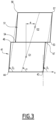
- the Z control pattern may exhibit a defect resulting from the translation of one array of lines relative to the other in a direction normal to the lines of an array, in the plane of that array (x direction).
- the upper line 51 is translated in the x direction by a distance e relative to the lower line 41.
- This translation defect is described by the angle ⁇ , or translation angle, between the normal direction x and the direction connecting the geometric centers G 1 and G 2 of a pair of lines.
- the control pattern may also have a defect resulting from the deformation of the lines of the line arrays, each line then having a diamond-shaped section (in other words, the side walls of a line are no longer at right angles to the bottom of this line).
- the edges between corners 44 and 46, on the one hand, and 43 and 47, on the other hand, of the lower line 41 are inclined
- the edges between corners 54 and 56, on the one hand, and 53 and 57, on the other hand, of the upper line 51 are inclined.
- a first edge angle ⁇ 1 as the angle between the x direction and the direction joining the lower right corner 43 of the first line 41 and the upper right corner 57 of the second line 51.
- a second edge angle ⁇ 2 is defined as the angle between the x direction and the direction joining the lower left corner 44 of the first line 41 and the upper left corner 56 of the second line 51.
- the method according to the invention makes it possible to quickly identify the nature of the defect affecting the control pattern.
- the method 100 makes it possible to classify a defect according to six possible cases or classes. Each of these cases is schematically represented at the bottom of the figure 4 .
- the measuring device figure 1 is implemented to acquire a diffraction pattern of the control area of a tested component.
- the diffraction pattern advantageously comprises only two Bragg rods. These two Bragg rods must be symmetrical to each other with respect to the q z axis. This is therefore the pair of Bragg rods of order -n and order n.
- a first test Q1 is carried out on the diffraction pattern acquired in step 105.
- This first test consists of checking whether the positions along the q z axis of the maxima of the Bragg rod of order -n are identical to the positions along the q z axis of the maxima of the Bragg rod of order n.
- the maxima considered here include at least the principal maximum q z n , o And q z ⁇ n , o Bragg rods of order n and -n and a secondary maximum q z n , i And q z ⁇ n , i Bragg rods of order n and -n. If so, the method proceeds to step 120 and if not, the method proceeds to step 130.
- a second test Q2 is performed on the diffraction pattern acquired in step 105.
- step 125 the measuring device figure 1 is activated to complete the diffraction pattern obtained in step 105 in order to obtain a third Bragg rod, for example the k-order rod.
- Step 125 is implemented only if, in step 105, this third rod has not already been acquired.
- a fourth test Q4 is performed on the completed diffraction pattern.
- This fourth test consists of checking whether the position along the q z axis of the i th extremum (minimum or maximum) changes as a function of the order. For example, q z ⁇ n , i , q z n , i And q z k , i are they in linear progression according to the order? If so, the process 100 stops and the pattern is considered to correspond to case 2. If not, the process stops and the defect is considered to correspond to case 1.
- step 130 a third test Q3 is applied to the diffraction pattern obtained in step 105 (which has at least the two Bragg rods of order -n and n).
- a fifth test Q5 is applied to the diffraction pattern.
- the numeral adjective associated with each of the tests of method 100 does not indicate the order in which this test is performed.
- the third test Q3 is applied only if the response to the first test Q1 is negative. This is then the second test that is actually applied to the diffraction pattern analyzed. In this alternative, the second and fourth tests, Q2 and Q4, are not applied. Depending on the response to this third test Q3, the fifth test Q5 will or will not be applied.
- FIG 5 represents the intensity profile of four Bragg rods recorded on a diffraction pattern obtained at the output of the device of the figure 1 .
- Curve C (-2) corresponds to the Bragg rod of order -2
- curve C (-1) corresponds to the rod of order -1
- curve C (1) corresponds to the rod of order 1
- curve C (2) corresponds to the rod of order 2.
- Step 105 allows for example the acquisition of curves C (2) and C (-2) .
- Step 125 allows the diffraction pattern to be completed with, for example, the acquisition of curves C (-1) and C (1) .
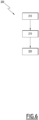
- the identification method 100 is advantageously integrated into a control method 200.
- the method 200 is implemented along a mass production line of a microelectronic component.
- the latter is a multi-level component comprising at least a first level and a second level.
- a control pattern is engraved on each component. This results from the superposition of a first network of lines produced during the manufacturing of the component on the first level and a second network of lines produced during the manufacturing on the second level.
- the method 200 is carried out on a first component.
- the identification method 100 is implemented. This makes it possible to determine the case to which the defect relates.
- step 220 the manufacturing conditions are adjusted according to the result of step 210, i.e. the type of defect identified.
- This adjustment of the manufacturing conditions may consist simply of modifying the operating parameters of the different devices along the manufacturing chain and of seeking to determine optimal manufacturing conditions progressively by a trial and error approach by iterating steps 210 and 220 on a succession of microelectronic components leaving the production chain.
- step 210 of identifying the type of defect is followed by a step 215 of measuring a value of at least one characteristic parameter of the defect affecting the pattern of the microelectronic component being checked.
- This measurement takes into account the result of step 210 in the choice of the most suitable instrumental method for acquiring measurement data with a view to extracting this characteristic parameter (if the data already acquired in steps 105 and 125 are not sufficient) and/or in the analysis method using suitable modeling to extract the value of the characteristic parameter considered from the measurement data.
- the chosen instrumental method is preferably a CD-SAXS technique, but other techniques can be used to carry out the acquisition of measurement data.
- the choice of the instrumental method also covers the definition of the part of the diffraction pattern that is necessary and sufficient to acquire to obtain the measurement data allowing a precise characterization of the defect.
- the part of the diffraction pattern to be acquired can, in turn, impact the instrumental device to be used for the precise measurement.
- the identification step 210 shows that the presence of overlay is characterized by an asymmetry along the q x axis
- the measurement of a single Bragg rod is sufficient.
- a point detector may be sufficient for a T-SAXS measurement.
- the measurement of several Bragg orders is necessary.
- a one-dimensional detector is used for a T-SAXS measurement.
- the adjustment step 220 takes into account the measured value of each characteristic parameter to adapt the manufacturing conditions and gradually lead to the manufacturing of a component whose control pattern does not contain any defects.
- CD-SAXS is a non-trivial characterization method
- the method according to the invention makes it possible to guide towards the appropriate analysis method of the diffraction pattern. It is independent of the modeling.
- the adapted modeling i.e. simplified compared to a complex modeling integrating all the characteristic parameters of all the potential defects
- the CD-SAXS control technique becomes particularly advantageous along a manufacturing line to, after each measurement of the overlay, realign the manufacturing equipment during the lithography process itself. This allows to correct the manufacturing accuracy during the operation of the manufacturing line.
Landscapes
- Physics & Mathematics (AREA)
- General Physics & Mathematics (AREA)
- Chemical & Material Sciences (AREA)
- Life Sciences & Earth Sciences (AREA)
- Crystallography & Structural Chemistry (AREA)
- Health & Medical Sciences (AREA)
- Electromagnetism (AREA)
- Analytical Chemistry (AREA)
- Biochemistry (AREA)
- General Health & Medical Sciences (AREA)
- Immunology (AREA)
- Pathology (AREA)
- Analysing Materials By The Use Of Radiation (AREA)
Applications Claiming Priority (1)
| Application Number | Priority Date | Filing Date | Title |
|---|---|---|---|
| FR2304035A FR3148089B1 (fr) | 2023-04-21 | 2023-04-21 | Procédé d’identification d’un défaut affectant un motif de contrôle porté par un composant microélectronique ; procédé de contrôle, système instrumental et produit programme d’ordinateur associés. |
Publications (3)
| Publication Number | Publication Date |
|---|---|
| EP4451060A1 true EP4451060A1 (de) | 2024-10-23 |
| EP4451060C0 EP4451060C0 (de) | 2025-11-26 |
| EP4451060B1 EP4451060B1 (de) | 2025-11-26 |
Family
ID=87554878
Family Applications (1)
| Application Number | Title | Priority Date | Filing Date |
|---|---|---|---|
| EP24171234.8A Active EP4451060B1 (de) | 2023-04-21 | 2024-04-19 | Verfahren zur identifizierung eines fehlers, der ein von einer mikroelektronischen komponente getragenes kontrollmuster beeinflusst, steuerverfahren, entsprechendes instrument und computerprogrammprodukt |
Country Status (2)
| Country | Link |
|---|---|
| EP (1) | EP4451060B1 (de) |
| FR (1) | FR3148089B1 (de) |
Citations (4)
| Publication number | Priority date | Publication date | Assignee | Title |
|---|---|---|---|---|
| US20070224518A1 (en) * | 2006-03-27 | 2007-09-27 | Boris Yokhin | Overlay metrology using X-rays |
| US20150117610A1 (en) | 2013-10-28 | 2015-04-30 | Kla-Tencor Corporation | Methods and apparatus for measuring semiconductor device overlay using x-ray metrology |
| US20160320319A1 (en) | 2015-04-28 | 2016-11-03 | Kla-Tencor Corporation | Computationally Efficient X-ray Based Overlay Measurement |
| EP4137889A1 (de) | 2021-08-20 | 2023-02-22 | ASML Netherlands B.V. | Metrologiemessverfahren und -vorrichtung |
-
2023
- 2023-04-21 FR FR2304035A patent/FR3148089B1/fr active Active
-
2024
- 2024-04-19 EP EP24171234.8A patent/EP4451060B1/de active Active
Patent Citations (4)
| Publication number | Priority date | Publication date | Assignee | Title |
|---|---|---|---|---|
| US20070224518A1 (en) * | 2006-03-27 | 2007-09-27 | Boris Yokhin | Overlay metrology using X-rays |
| US20150117610A1 (en) | 2013-10-28 | 2015-04-30 | Kla-Tencor Corporation | Methods and apparatus for measuring semiconductor device overlay using x-ray metrology |
| US20160320319A1 (en) | 2015-04-28 | 2016-11-03 | Kla-Tencor Corporation | Computationally Efficient X-ray Based Overlay Measurement |
| EP4137889A1 (de) | 2021-08-20 | 2023-02-22 | ASML Netherlands B.V. | Metrologiemessverfahren und -vorrichtung |
Also Published As
| Publication number | Publication date |
|---|---|
| FR3148089B1 (fr) | 2025-09-19 |
| FR3148089A1 (fr) | 2024-10-25 |
| EP4451060C0 (de) | 2025-11-26 |
| EP4451060B1 (de) | 2025-11-26 |
Similar Documents
| Publication | Publication Date | Title |
|---|---|---|
| EP1580524B1 (de) | Verfahren und Vorrichtung zur Charakterisierung von Strukturschäden mittels Moiré- Schatten | |
| EP0209457B1 (de) | Verfahren und Vorrichtung zur Bestimmung der Güte eines optischen Instruments, insbesondere der Übertragungsfunktion | |
| EP3754431B1 (de) | Holografisches rekonstruktionsverfahren | |
| KR101547459B1 (ko) | 위상 축소 이미징 시스템 및 이를 이용한 이미징 방법 | |
| EP4451060B1 (de) | Verfahren zur identifizierung eines fehlers, der ein von einer mikroelektronischen komponente getragenes kontrollmuster beeinflusst, steuerverfahren, entsprechendes instrument und computerprogrammprodukt | |
| WO2023187171A1 (fr) | Procédé et système de caractérisation d'un objectif optique pour la correction d'aberrations optiques introduites par ledit objectif optique dans une image | |
| EP4246135B1 (de) | Verbessertes verfahren zur messung der ausrichtung eines zeilenablenkungsfehlers in kleinen winkeln durch t-saxs-übertragung ; entsprechendes instrumentalsystem und computerprogrammprodukt | |
| EP1682879B1 (de) | Verwendung einer optischen fourier-transformation zur einhaltung der grössentoleranz in der mikroelektronik | |
| EP2054696A1 (de) | Verfahren für kontaktlose messung zweischichtiger dreidimensionaler objekte mittels optischer einzelansichts-ombroskopie | |
| KR20210125428A (ko) | 광학 측정 시스템 및 광학 측정 방법 | |
| FR3071611A1 (fr) | Procede et dispositif de controle non destructif d'une piece aeronautique | |
| EP4421482B1 (de) | Verfahren zur t-sax-messung eines abdeckungsfehlers, der ein durch eine mikroelektronische komponente getragenes kontrollmuster beeinflussen, entsprechendes instrumentalsystem und computerprogrammprodukt | |
| FR3141245A1 (fr) | Procédé d’analyse tomographique | |
| JP6196841B2 (ja) | 透過波面計測装置及び透過波面計測方法 | |
| EP4575474A1 (de) | Verfahren zur messung eines überlagerungsfehlers, entsprechendes instrumentalsystem und computerprogrammprodukt | |
| EP4419866A1 (de) | Verfahren zur funktionellen charakterisierung optischer linsen | |
| FR3141240A1 (fr) | Procédé de caractérisation fonctionnelle d’objectifs optiques d’appareils d’imagerie médicale | |
| FR3141243A1 (fr) | Procédé de caractérisation fonctionnelle d’objectifs optiques de Smartphone | |
| EP4433792A1 (de) | Verfahren zur herstellung eines geometrischen charakterisierungswerkzeugs für eine optische linse zur herstellung | |
| EP3617646B1 (de) | Messmethode der linienrauheit eines liniennetzes durch beugung von röntgenstrahlen | |
| US20260009637A1 (en) | Coherent spectroscopy for tsv | |
| EP4390382A1 (de) | Messverfahren mit röntgenkleinwinkelstreuung unter streifendem einfall; entsprechendes instrumentalsystem und computerprogrammprodukt | |
| CN110715931B (zh) | 一种透明样品缺陷自动检测方法和检测装置 | |
| EP4217727A1 (de) | Kalibrierungsverfahren für an zylinderartige strukturen angepasste geführte elastische wellentomografie |
Legal Events
| Date | Code | Title | Description |
|---|---|---|---|
| PUAI | Public reference made under article 153(3) epc to a published international application that has entered the european phase |
Free format text: ORIGINAL CODE: 0009012 |
|
| STAA | Information on the status of an ep patent application or granted ep patent |
Free format text: STATUS: REQUEST FOR EXAMINATION WAS MADE |
|
| 17P | Request for examination filed |
Effective date: 20240419 |
|
| AK | Designated contracting states |
Kind code of ref document: A1 Designated state(s): AL AT BE BG CH CY CZ DE DK EE ES FI FR GB GR HR HU IE IS IT LI LT LU LV MC ME MK MT NL NO PL PT RO RS SE SI SK SM TR |
|
| RAP3 | Party data changed (applicant data changed or rights of an application transferred) |
Owner name: COMMISSARIAT A L'ENERGIE ATOMIQUE ET AUX ENERGIESALTERNATIVES |
|
| GRAP | Despatch of communication of intention to grant a patent |
Free format text: ORIGINAL CODE: EPIDOSNIGR1 |
|
| STAA | Information on the status of an ep patent application or granted ep patent |
Free format text: STATUS: GRANT OF PATENT IS INTENDED |
|
| RIC1 | Information provided on ipc code assigned before grant |
Ipc: G03F 7/00 20060101AFI20250731BHEP Ipc: H01L 21/66 20060101ALI20250731BHEP Ipc: G01N 23/201 20180101ALI20250731BHEP Ipc: G01B 15/06 20060101ALI20250731BHEP |
|
| INTG | Intention to grant announced |
Effective date: 20250828 |
|
| GRAS | Grant fee paid |
Free format text: ORIGINAL CODE: EPIDOSNIGR3 |
|
| GRAA | (expected) grant |
Free format text: ORIGINAL CODE: 0009210 |
|
| STAA | Information on the status of an ep patent application or granted ep patent |
Free format text: STATUS: THE PATENT HAS BEEN GRANTED |
|
| AK | Designated contracting states |
Kind code of ref document: B1 Designated state(s): AL AT BE BG CH CY CZ DE DK EE ES FI FR GB GR HR HU IE IS IT LI LT LU LV MC ME MK MT NL NO PL PT RO RS SE SI SK SM TR |
|
| REG | Reference to a national code |
Ref country code: CH Ref legal event code: F10 Free format text: ST27 STATUS EVENT CODE: U-0-0-F10-F00 (AS PROVIDED BY THE NATIONAL OFFICE) Effective date: 20251126 Ref country code: GB Ref legal event code: FG4D Free format text: NOT ENGLISH |
|
| REG | Reference to a national code |
Ref country code: IE Ref legal event code: FG4D Free format text: LANGUAGE OF EP DOCUMENT: FRENCH |
|
| U01 | Request for unitary effect filed |
Effective date: 20251128 |
|
| U07 | Unitary effect registered |
Designated state(s): AT BE BG DE DK EE FI FR IT LT LU LV MT NL PT RO SE SI Effective date: 20251208 |
|
| PG25 | Lapsed in a contracting state [announced via postgrant information from national office to epo] |
Ref country code: ES Free format text: LAPSE BECAUSE OF FAILURE TO SUBMIT A TRANSLATION OF THE DESCRIPTION OR TO PAY THE FEE WITHIN THE PRESCRIBED TIME-LIMIT Effective date: 20251126 |
|
| PG25 | Lapsed in a contracting state [announced via postgrant information from national office to epo] |
Ref country code: NO Free format text: LAPSE BECAUSE OF FAILURE TO SUBMIT A TRANSLATION OF THE DESCRIPTION OR TO PAY THE FEE WITHIN THE PRESCRIBED TIME-LIMIT Effective date: 20260226 |
|
| PG25 | Lapsed in a contracting state [announced via postgrant information from national office to epo] |
Ref country code: HR Free format text: LAPSE BECAUSE OF FAILURE TO SUBMIT A TRANSLATION OF THE DESCRIPTION OR TO PAY THE FEE WITHIN THE PRESCRIBED TIME-LIMIT Effective date: 20251126 |
|
| PG25 | Lapsed in a contracting state [announced via postgrant information from national office to epo] |
Ref country code: RS Free format text: LAPSE BECAUSE OF FAILURE TO SUBMIT A TRANSLATION OF THE DESCRIPTION OR TO PAY THE FEE WITHIN THE PRESCRIBED TIME-LIMIT Effective date: 20260226 |
|
| PG25 | Lapsed in a contracting state [announced via postgrant information from national office to epo] |
Ref country code: IS Free format text: LAPSE BECAUSE OF FAILURE TO SUBMIT A TRANSLATION OF THE DESCRIPTION OR TO PAY THE FEE WITHIN THE PRESCRIBED TIME-LIMIT Effective date: 20260326 |
|
| PG25 | Lapsed in a contracting state [announced via postgrant information from national office to epo] |
Ref country code: PL Free format text: LAPSE BECAUSE OF FAILURE TO SUBMIT A TRANSLATION OF THE DESCRIPTION OR TO PAY THE FEE WITHIN THE PRESCRIBED TIME-LIMIT Effective date: 20251126 |