EP4506991A1 - Verfahren zur herstellung einer mikroelektronischen vorrichtung auf der basis eines halbmetall-materials - Google Patents
Verfahren zur herstellung einer mikroelektronischen vorrichtung auf der basis eines halbmetall-materials Download PDFInfo
- Publication number
- EP4506991A1 EP4506991A1 EP24193483.5A EP24193483A EP4506991A1 EP 4506991 A1 EP4506991 A1 EP 4506991A1 EP 24193483 A EP24193483 A EP 24193483A EP 4506991 A1 EP4506991 A1 EP 4506991A1
- Authority
- EP
- European Patent Office
- Prior art keywords
- semi
- metallic material
- layer
- openings
- layers
- Prior art date
- Legal status (The legal status is an assumption and is not a legal conclusion. Google has not performed a legal analysis and makes no representation as to the accuracy of the status listed.)
- Pending
Links
Images










Classifications
-
- H—ELECTRICITY
- H10—SEMICONDUCTOR DEVICES; ELECTRIC SOLID-STATE DEVICES NOT OTHERWISE PROVIDED FOR
- H10D—INORGANIC ELECTRIC SEMICONDUCTOR DEVICES
- H10D84/00—Integrated devices formed in or on semiconductor substrates that comprise only semiconducting layers, e.g. on Si wafers or on GaAs-on-Si wafers
- H10D84/01—Manufacture or treatment
- H10D84/02—Manufacture or treatment characterised by using material-based technologies
-
- H—ELECTRICITY
- H10—SEMICONDUCTOR DEVICES; ELECTRIC SOLID-STATE DEVICES NOT OTHERWISE PROVIDED FOR
- H10D—INORGANIC ELECTRIC SEMICONDUCTOR DEVICES
- H10D30/00—Field-effect transistors [FET]
- H10D30/01—Manufacture or treatment
- H10D30/019—Manufacture or treatment of FETs having stacked nanowire, nanosheet or nanoribbon channels
- H10D30/0191—Manufacture or treatment of FETs having stacked nanowire, nanosheet or nanoribbon channels forming stacked channels, e.g. changing their shapes or sizes
-
- H—ELECTRICITY
- H10—SEMICONDUCTOR DEVICES; ELECTRIC SOLID-STATE DEVICES NOT OTHERWISE PROVIDED FOR
- H10D—INORGANIC ELECTRIC SEMICONDUCTOR DEVICES
- H10D30/00—Field-effect transistors [FET]
- H10D30/01—Manufacture or treatment
- H10D30/014—Manufacture or treatment of FETs having zero-dimensional [0D] or one-dimensional [1D] channels, e.g. quantum wire FETs, single-electron transistors [SET] or Coulomb blockade transistors
-
- H—ELECTRICITY
- H10—SEMICONDUCTOR DEVICES; ELECTRIC SOLID-STATE DEVICES NOT OTHERWISE PROVIDED FOR
- H10D—INORGANIC ELECTRIC SEMICONDUCTOR DEVICES
- H10D30/00—Field-effect transistors [FET]
- H10D30/40—FETs having zero-dimensional [0D], one-dimensional [1D] or two-dimensional [2D] charge carrier gas channels
- H10D30/43—FETs having zero-dimensional [0D], one-dimensional [1D] or two-dimensional [2D] charge carrier gas channels having one-dimensional [1D] charge carrier gas channels, e.g. quantum wire FETs or transistors having 1D quantum-confined channels
-
- H—ELECTRICITY
- H10—SEMICONDUCTOR DEVICES; ELECTRIC SOLID-STATE DEVICES NOT OTHERWISE PROVIDED FOR
- H10D—INORGANIC ELECTRIC SEMICONDUCTOR DEVICES
- H10D30/00—Field-effect transistors [FET]
- H10D30/501—FETs having stacked nanowire, nanosheet or nanoribbon channels
- H10D30/502—FETs having stacked nanowire, nanosheet or nanoribbon channels characterised by the stacked channels
-
- H—ELECTRICITY
- H10—SEMICONDUCTOR DEVICES; ELECTRIC SOLID-STATE DEVICES NOT OTHERWISE PROVIDED FOR
- H10D—INORGANIC ELECTRIC SEMICONDUCTOR DEVICES
- H10D62/00—Semiconductor bodies, or regions thereof, of devices having potential barriers
- H10D62/10—Shapes, relative sizes or dispositions of the regions of the semiconductor bodies; Shapes of the semiconductor bodies
- H10D62/117—Shapes of semiconductor bodies
- H10D62/118—Nanostructure semiconductor bodies
- H10D62/119—Nanowire, nanosheet or nanotube semiconductor bodies
- H10D62/121—Nanowire, nanosheet or nanotube semiconductor bodies oriented parallel to substrates
-
- H—ELECTRICITY
- H10—SEMICONDUCTOR DEVICES; ELECTRIC SOLID-STATE DEVICES NOT OTHERWISE PROVIDED FOR
- H10D—INORGANIC ELECTRIC SEMICONDUCTOR DEVICES
- H10D62/00—Semiconductor bodies, or regions thereof, of devices having potential barriers
- H10D62/80—Semiconductor bodies, or regions thereof, of devices having potential barriers characterised by the materials
-
- H—ELECTRICITY
- H10—SEMICONDUCTOR DEVICES; ELECTRIC SOLID-STATE DEVICES NOT OTHERWISE PROVIDED FOR
- H10D—INORGANIC ELECTRIC SEMICONDUCTOR DEVICES
- H10D84/00—Integrated devices formed in or on semiconductor substrates that comprise only semiconducting layers, e.g. on Si wafers or on GaAs-on-Si wafers
- H10D84/80—Integrated devices formed in or on semiconductor substrates that comprise only semiconducting layers, e.g. on Si wafers or on GaAs-on-Si wafers characterised by the integration of at least one component covered by groups H10D12/00 or H10D30/00, e.g. integration of IGFETs
- H10D84/82—Integrated devices formed in or on semiconductor substrates that comprise only semiconducting layers, e.g. on Si wafers or on GaAs-on-Si wafers characterised by the integration of at least one component covered by groups H10D12/00 or H10D30/00, e.g. integration of IGFETs of only field-effect components
- H10D84/83—Integrated devices formed in or on semiconductor substrates that comprise only semiconducting layers, e.g. on Si wafers or on GaAs-on-Si wafers characterised by the integration of at least one component covered by groups H10D12/00 or H10D30/00, e.g. integration of IGFETs of only field-effect components of only insulated-gate FETs [IGFET]
-
- H—ELECTRICITY
- H10—SEMICONDUCTOR DEVICES; ELECTRIC SOLID-STATE DEVICES NOT OTHERWISE PROVIDED FOR
- H10D—INORGANIC ELECTRIC SEMICONDUCTOR DEVICES
- H10D84/00—Integrated devices formed in or on semiconductor substrates that comprise only semiconducting layers, e.g. on Si wafers or on GaAs-on-Si wafers
- H10D84/01—Manufacture or treatment
- H10D84/0123—Integrating together multiple components covered by H10D12/00 or H10D30/00, e.g. integrating multiple IGBTs
- H10D84/0126—Integrating together multiple components covered by H10D12/00 or H10D30/00, e.g. integrating multiple IGBTs the components including insulated gates, e.g. IGFETs
- H10D84/0128—Manufacturing their channels
-
- H—ELECTRICITY
- H10—SEMICONDUCTOR DEVICES; ELECTRIC SOLID-STATE DEVICES NOT OTHERWISE PROVIDED FOR
- H10D—INORGANIC ELECTRIC SEMICONDUCTOR DEVICES
- H10D84/00—Integrated devices formed in or on semiconductor substrates that comprise only semiconducting layers, e.g. on Si wafers or on GaAs-on-Si wafers
- H10D84/01—Manufacture or treatment
- H10D84/02—Manufacture or treatment characterised by using material-based technologies
- H10D84/03—Manufacture or treatment characterised by using material-based technologies using Group IV technology, e.g. silicon technology or silicon-carbide [SiC] technology
- H10D84/038—Manufacture or treatment characterised by using material-based technologies using Group IV technology, e.g. silicon technology or silicon-carbide [SiC] technology using silicon technology, e.g. SiGe
Definitions
- the present invention relates to the field of microelectronics technologies. It finds a particularly advantageous application in the manufacture of advanced FET ("Field-Effect Transistor") type devices whose conduction channels are based on a semi-metallic material.
- FET Field-Effect Transistor
- the document US2018/0190799 A1 discloses another manufacturing method integrating a semi-metallic material into a conformal gate transistor.
- a vertical arrangement of the channels is disclosed in this document.
- a bismuth-based semi-metallic layer is deposited in holes having nanometric dimensions to form the semiconductor channels in the form of vertical nanowires.
- the semi-metallic layer opens out of the holes to form source or drain regions. These source/drain regions have dimensions larger than those of the channels, and have a metallic character.
- Such a method exploiting the semi-metal/semiconductor transition by geometric constriction is suitable for industrial exploitation.
- the formation of holes having nanometric dimensions is difficult to control.
- the integration densities accessible by this method remain limited.
- the document FR3095549 discloses another method for producing a transistor based on a semi-metallic material in a planar arrangement.
- the production of such an architecture is simpler and more reliable.
- a "mold" defining the patterns intended to form the channels and the source and drain regions and their contacts is here previously produced.
- the semi-metallic material is then deposited in this mold, then thinned by polishing. This makes it easier to obtain dimensions giving the channels a semiconductor character.
- the integration density remains limited.
- the electrostatic control of the transistors is also limited.
- the present invention proposes to overcome at least in part the drawbacks of known methods and architectures.
- one objective of the present invention is to propose a device making it possible to increase the integration density of transistors based on a semi-metallic material.
- Another objective of the present invention is to propose a method for manufacturing such a device.
- the enclosing grid completely surrounds at least one of the channels, and preferably several channels of the plurality of channels, in a transverse plane yz. perpendicular to the longitudinal direction x.
- Such a gate-all-around architecture is called GAA (acronym for Gate All Around), and comprises channels stacked on top of each other in a so-called vertical direction z, surrounded by a common gate.
- GAA cronym for Gate All Around
- the device can comprise at least two adjacent transistors in a horizontal direction, each transistor comprising channels stacked in the vertical direction z.
- Such a device architecture advantageously exceeds the performance of known transistor architectures based on a semi-metallic material.
- a principle of the method according to the invention consists in selectively replacing certain layers of the initial stack with the semi-metallic material in order to form the channels of the transistor.
- the deposition of the semi-metallic material advantageously forms the channels and at least one of the drain or source contacts in a single step.
- the initial stack does not include the semi-metallic material.
- the subsequent deposition of the semi-metallic material aims to better preserve the semi-metallic material.
- the layers of semi-metallic material are introduced at the end of the process, after structuring the stack and typically after the formation of the spacers and the encapsulating grid. This advantageously limits the risk of degradation of the semi-metallic material during the process.
- the semi-metallic material is not exposed at all stages of the manufacturing process. The semi-metallic material is thus preserved.
- the late introduction of the semi-metallic material during the manufacturing process allows the use of standard microelectronics technologies for the formation and structuring of the stack. It is not necessary to modify or adapt the standard technological structuring steps to the constraints of using the semi-metallic material. The process costs are thus advantageously limited. The process can also be more easily implemented in existing production lines.
- section planes are indicated (A-A', B-B', ..., T-T') with cross-references to the section planes of the corresponding figures.
- the drawings are given as examples and do not limit the invention. They constitute schematic representations of principle intended to facilitate understanding of the invention and are not necessarily to the scale of practical applications. In particular, in the principle diagrams, the thicknesses and/or dimensions of the different layers, patterns and reliefs are not representative of reality. For reasons of clarity, all of the alphanumeric references are not systematically repeated from one figure to another. It is understood that the elements already described and referenced, when they are reproduced in another figure, typically bear the same alphanumeric references, even if these are not explicitly mentioned. A person skilled in the art will easily identify the same element reproduced in different figures.
- the device comprises at least two transistors arranged in a first direction x or y called horizontal, and the channels of each transistor are stacked in a second direction z called vertical, perpendicular to the first x or y direction.
- one of the source and drain contacts is made of the semi-metallic material and the other of the source and drain contacts is made of a metal.
- the semi-metallic material is based on at least one element among bismuth (Bi), tin (Sn), antimony (Sb), arsenic (As).
- the first patterns extend primarily in the longitudinal direction x, and the second patterns extend primarily in a transverse direction y.
- the wrapping gate is formed before the deposition of the layer based on the semi-metallic material. This corresponds to a "gate first" type process (the replacement of the sacrificial gate by a functional gate is done before the formation of the transistor channels).
- the formation of the gate dielectric layer is formed after complete removal of the first material from the first layers and before formation of the wrapping gate, by depositing a dielectric layer in the cavities and in the third openings, on the exposed portions of the second layers.
- the formation of the spacers and the formation of the gate dielectric layer are performed at least in part by a single deposition of a dielectric layer in the cavities. This makes it possible to reduce the number of process steps and/or to thicken the spacers.
- the deposition of the layer based on the semi-metallic material is carried out in the second spaces and in all the second openings so as to form the channels and all the source and drain contacts.
- the number of steps of the method is advantageously reduced.
- the method further comprises, after deposition of the base layer semi-metallic material, crystallization annealing.
- the layer based on the semi-metallic material is coated prior to the crystallization annealing, and the crystallization annealing is carried out at a temperature above the melting temperature of the semi-metallic material.
- the second openings are reformed by successively exposing a single flank of the second layers, and the deposition of the layer based on the semi-metallic material forms a single contact among the source and drain contacts.
- the other contact of the source and drain contacts is a metal contact formed by depositing a metal layer in a portion of the second openings.
- the deposition of the layer based on the semi-metallic material is carried out by growth, preferably by epitaxy, from exposed areas of said metallic contact through the second spaces.
- the invention relates generally to a method of manufacturing a microelectronic device with GAA transistors, based on a semi-metallic material.
- a microelectronic device can have a "GAA stacked nanosheet” type architecture, i.e. with stacked nanosheets and a fully encapsulating gate.
- An architecture with stacked nanowires and a fully encapsulating gate is also possible.
- Nanowires or nanosheets typically each comprise a conduction channel of a transistor. These channels are stacked in a z direction. This means that they each occupy a level of given altitude in the z direction. A level can be defined between two planes perpendicular to the z direction.
- the method according to the invention can be implemented for the production of GAA MOS transistors for the 5 nm and sub-5 nm technological nodes.
- a microelectronic device comprising GAA transistors can be advantageously integrated into logic systems having 3D architectures. These transistors can in particular be associated with other structural or functional elements so as to design complex systems.
- a particular aspect of the invention concerns the use of semi-metallic materials to produce the nanowires or nanosheets of the device.
- These semi-metallic materials may have properties of a metal or a semiconductor, typically depending on the temperature or a dimensional confinement.
- the band structure of the semi-metallic or semi-metallic materials brings them closer to metals, insofar as these materials do not have a band gap, but the low density of electronic states at the Fermi level splits the carriers into two populations, electrons and holes, as for semiconductors.
- the semi-metallic materials are preferably based on bismuth (Bi), tin (Sn), antimony (Sb), arsenic (As), tellurium (Te).
- Other materials having semi-metallic properties, at least under certain conditions, are also conceivable.
- Some alloys may be semi-metallic, such as mercury telluride HgTe.
- Some conductive polymers may have semi-metallic phases; some thin-film graphene structures, for example, may be semi-metallic depending on their magnetic environment.
- the terms “on”, “surmounts”, “covers”, “underlying”, “facing” and their equivalents do not necessarily mean “in contact with”.
- the deposition or application of a first layer on a second layer does not necessarily mean that the two layers are directly in contact with each other, but means that the first layer at least partially covers the second layer by being either directly in contact with it or by being separated from it by at least one other layer or at least one other element.
- a substrate, film or layer “based on” a material A means a substrate, film or layer comprising this material A only or this material A and possibly other materials, for example doping elements or alloying elements.
- a silicon nitride SiN spacer may for example comprise non-stoichiometric silicon nitride (SiN), or stoichiometric silicon nitride (Si3N4), or even a silicon oxynitride (SiON).
- dielectric describes a material whose electrical conductivity is sufficiently low in the given application to serve as an insulator.
- a dielectric material preferably has a dielectric constant of less than 20.
- step means the performance of a part of the process, and can designate a set of sub-steps.
- step does not necessarily mean that the actions carried out during a step are simultaneous or immediately successive. Certain actions of a first step may in particular be followed by actions linked to a different step, and other actions of the first step may be repeated subsequently. Thus, the term step does not necessarily mean actions that are unitary and inseparable in time and in the sequence of the phases of the process.
- Selective etching with respect to or “etching having selectivity with respect to” means an etching configured to remove a material A or a layer A with respect to a material B or a layer B, and having an etching rate of the material A greater than the etching rate of the material B.
- the selectivity is the ratio between the etching rate of the material A and the etching rate of the material B. It is denoted S A:B .
- a selectivity S A:B of 10:1 means that the etching rate of the material A is 10 times greater than the etching rate of the material B.
- the various patterns formed during the manufacturing steps typically have a structure intended to evolve during the process steps.
- the patterns may comprise the sacrificial layers of the initial stack, the layers based on semi-metallic material, the dielectric layers, continuous or discontinuous.
- the various patterns aim to form, at the end of the process, “transistor patterns” each comprising at least one conduction channel and a gate surrounding said channel, a dielectric barrier separating the gate and the channel, a source and a drain on either side of the channel.
- Transistor patterns each comprising at least one conduction channel and a gate surrounding said channel, a dielectric barrier separating the gate and the channel, a source and a drain on either side of the channel.
- a preferably orthonormal reference frame comprising the x, y, z axes, is shown in the attached figures.
- a layer or a film typically has a thickness along z.
- a grid pattern formed on such a surface layer has a height along z.
- the relative terms “on”, “surmounts”, “under”, “underlying” refer to positions taken along the z direction.
- a “lateral” dimension corresponds to a dimension along a direction of the xy plane.
- a “lateral” or “laterally” extension means an extension along one or more directions of the xy plane.
- the longitudinal direction corresponds to the direction in which the channel of a transistor extends, between the source and the drain.
- the longitudinal direction is directed along x in the illustrative figures.
- a transverse direction is directed along y or z.
- a transverse dimension is typically taken along y or z.
- the thickness of the layer forming the channel is a transverse dimension of the channel.
- An element located "perpendicular to” or “in line with” another element means that these two elements are both located on the same line perpendicular to a plane in which a lower or upper face of a substrate mainly extends, that is to say on the same line oriented vertically in the cross-sectional figures.
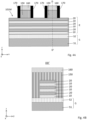
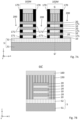
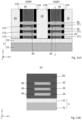
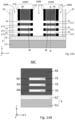
- Figures 1A, 1B to 15A, 15B schematically illustrate steps in manufacturing a device comprising GAA transistors based on a semi-metallic material, according to a first embodiment.
- a first step consists in producing a stack E of semiconductor layers 10, 20 on a substrate S.
- the substrate S may be a substrate of the SOI (Silicon On Insulator), GeOI (Germanium On Insulator) or SGOI (Silicon-Germanium On Insulator) type. These substrates are grouped under the name "semiconductor-on-insulator". These known substrates comprise, according to the terminology commonly used by those skilled in the art, a thick silicon support layer S1 called "Si bulk", an insulating layer S2 of silicon oxide called "BOX" (Burried Oxide) and a thin surface layer, respectively based on silicon, germanium or silicon-germanium.
- SOI Silicon On Insulator
- GeOI Germanium On Insulator
- SGOI Silicon-Germanium On Insulator
- This thin surface layer may advantageously correspond to the first layer 10 of the stack E.
- the final device comprising GAA transistors based on a semi-metallic material rests on the insulating layer (BOX) of the semiconductor-on-insulator type substrate.
- the substrate S can be a bulk Si substrate.
- Stack E comprises, according to one example, an alternation of first layers 10 in silicon-germanium (SiGe) and second layers 20 in silicon (Si).
- the concentration of Ge in the SiGe alloy can be 20%, 30% or 45% for example.
- This concentration of germanium is chosen so as to allow good selectivity of the etching of the SiGe relative to the Si, during the selective etching steps. The higher the concentration of Ge, the greater the selectivity to Si will be during the subsequent removal of the SiGe.
- This stack E is advantageously formed by epitaxy of the SiGe 10 and Si 20 layers. This step of forming the stack E is inexpensive and well known to those skilled in the art.
- the thicknesses of the Si and SiGe layers can be between 5 nm and 20 nm, and preferably between 4 nm and 10 nm. In a known manner in order to avoid the formation of structural defects, the maximum thicknesses permitted for the SiGe 10 layers depend in particular on the chosen Ge concentration.
- the first material of the first layers 10 and the second material of the second layers 20 are chosen so that one can be selectively etched relative to the other.
- the first and second materials can be chosen from dielectric materials (oxides and nitrides for example), semiconductor materials, and metallic materials.
- a conventional lithography/etching step is performed in order to define first 101M patterns, and first 100 openings.
- the etching is anisotropic and directed along z. It is configured to etch the stack E, here the Si/SiGe superlattice, over its entire height, stopping on the substrate S, here the BOX S2. It can be performed by plasma using HBr/O2 etching chemistry.
- the first 101M patterns can have a length L 1 along x of between 10 nm and 500 nm. They preferably have a width I 1 along y of between 5 nm and 20 nm. This first structuring of the E stack in the form of fins or “fins” according to current Anglo-Saxon terminology, makes it possible to define a plurality of superimposed nanowires or nanosheets.
- sacrificial grids 150 are then formed on the “end” patterns 101M.
- the formation of these sacrificial grids 150 is typically done by deposition and then lithography/etching.
- the formation of the sacrificial grids 150 is configured such that the sacrificial grids 150 straddle the “end” patterns 101M, as illustrated in Figure 3B .
- the sacrificial gates 150 typically comprise an upper portion located on the “end” pattern 101M, and lateral portions located on the lateral flanks of the “end” pattern 101M.
- the sacrificial gates 150 typically bear on the substrate S.
- the sacrificial gates 150 are typically surmounted by an etching mask 160, called a hard mask, implemented in the structuring of the sacrificial gates 150.
- the sacrificial gates 150 are for example based on polycrystalline silicon.
- a thin layer of SiO 2 oxide for example 7 nm thick, is preferably deposited prior to the formation of the sacrificial gates 150. This thin layer of SiO 2 oxide (not illustrated in the figures) is thus intercalated between the sacrificial gates 150 and the “end” patterns 101M. This thin layer of SiO 2 oxide can form a stop layer for the subsequent etching of the sacrificial gates 150.
- first spacers 170 are then formed on the yz-oriented flanks of the sacrificial grids 150. In general, in z projection, these spacers form a continuous ring around each sacrificial grid 150, with a closed contour. In cross-section, however, along the xz plane illustrated in Figure 4A , the first spacer 170 has two facing portions on each of the sides of the sacrificial gate 150. These two portions are generally designated as being the first spacers 170, even if they can be considered as belonging to a single spacer.
- the first spacers 170 typically extend to an upper face of the hard masks 160.
- the first spacers 170 are typically based on silicon nitride SiN or a dielectric material with a low dielectric constant, for example based on SiCO.
- the anisotropic etching along z is extended in order to define second patterns 102M, and second openings 200.
- the etching is configured to etch the E stack over its entire height, stopping on the S substrate. It can be carried out by plasma using HBr/O2 etching chemistry.
- the first layers 10 are partially etched selectively to the second layers 20, to the substrate S and to the first spacers 170.
- the etching of the first material of the first layers 10 typically has a selectivity S 10:20 relative to the second material of the second layers 20, of at least 5:1, preferably at least 10:1.
- This partial etching aims to form first spaces 11 directly above the first spacers 170.
- This partial etching is typically stopped in time. It has an isotropic character and can be carried out wet or dry, from the second openings 200. At the end of this partial etching, central parts of the first layers 10 are preserved under the sacrificial gates 150.
- the first spaces 11 are then filled with a dielectric material, for example with silicon nitride or with a low permittivity dielectric, to form internal spacers 171.
- a dielectric material for example with silicon nitride or with a low permittivity dielectric.
- These “internal” spacers 171 are integrated into the stack E, preferably directly above the first spacers 170. They are in contact with the central parts of the first layers 10.
- the formation of the internal spacers 171 is typically done from the second openings 200.
- This retaining layer 25 is then planarized, typically by chemical-mechanical polishing CMP with stopping on the hard masks 160.
- the hard masks 160 are first removed, then the sacrificial gates 150 are also removed.
- This removal can be carried out by wet etching with a stop on the thin stop layer based on SiO2 or another dielectric.
- This wet etching typically has a high selectivity with respect to the stop layer and the first spacers 170.
- This wet etching can be based on a solution of TMAH (Tetramethylammonium hydroxide) or TEAH (Tetraethylammonium Hydroxide) ammonia salts.
- TMAH Tetramethylammonium hydroxide
- TEAH Tetraethylammonium Hydroxide
- the central parts of the first layers 10 are then completely selectively etched to the second layers 20, to the internal spacers 171, and to the substrate S from the third openings 300.
- This etching aims to form cavities 21 in place of the central parts of the first layers 10.
- This total etching can be stopped in time, possibly after an over-etching time aimed at guaranteeing the total removal of the first material from the first layers 10.
- This total etching has an isotropic character and can be carried out by wet or dry means, from the third openings 300.
- the second layers 20 are held by the spacers 170, 171 and by a holding layer 25, as illustrated in FIG. Figure 10A .
- An advantageous step not illustrated in the figures consists in oxidizing the exposed parts of the second layers 20 from the third openings 300 and the cavities 21. This makes it possible to reduce the thickness along z and the lateral dimensions along y of the second material of the second layers 20. After replacing the second material of the second layers 20 to form the channels of the transistors, this makes it possible to ultimately obtain channels having reduced dimensions along z and along y.
- the channels of the transistors can thus have dimensions along z and along y of the order of a few nanometers.
- a dielectric layer 30 is then deposited in the cavities 21 from the openings 300.
- This dielectric layer 30 is typically based on a high permittivity material, for example based on HfO2.
- the dielectric layer 30 is typically intended to form the gate dielectric layer between the channels of the GAA transistors and their surrounding gates. It can be formed by chemical vapor deposition CVD (acronym for “Chemical Vapor Deposition”), by chemical vapor deposition with organometallic precursors MOCVD (acronym for “Metal Organic Chemical Vapor Deposition”) or by atomic layer deposition ALD (acronym for “Atomic Layer Deposition”).
- the dielectric layer 30 typically has a thickness of between 1 nm and 5 nm.
- the third openings 300 and the cavities 21 are then filled with one or more metal layers 50, for example based on TiN, W, in order to form the surrounding gates of the GAA transistors.
- metal layers 50 for example based on TiN, W
- a dielectric layer based on a high permittivity material for example based on HfO2
- a chemical mechanical polishing CMP is typically carried out in order to remove the excess metal deposited on the 102M patterns.
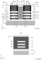
- FIGS. 13A, 13B , 14A, 14B , 14C , 15A and 15B schematically illustrate, according to the first embodiment, the sequence of manufacturing steps of the method allowing the production of the device comprising stacked channel GAA transistors based on a semi-metallic material.
- the holding layer 25 is opened by etching so as to partially reform the second openings 200b.
- These second openings 200b define the regions of the source and drain contacts.
- the two flanks along yz of each pattern 102M are exposed through these second openings 200b.
- the second layers 20 are then completely removed by selective etching with respect to the gate 50, the dielectric layer 30 and the spacers 170, 171.
- This etching can be stopped in time, possibly after an over-etching time intended to guarantee the total removal of the second material from the second layers 20.
- This total etching has an isotropic character and can be carried out by a wet or dry method, from the second openings 200b.
- second spaces 31 are formed in place of the second layers 20.
- the second openings 200b define the locations of the source and drain contacts.
- the second spaces 31 define the locations of the channels, drains and sources.
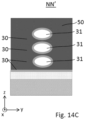
- FIG 14C illustrates a variant in which the section of the second spaces 31, and consequently of the channels of the transistors, is round or ovoid.
- a rounded shape can be obtained by oxidation of the second layers 20 after formation of the third openings 300 (removal of the sacrificial gate) and the cavities 21 illustrated in Figure 10A .
- this section may adopt one of the following geometric shapes: rectangular as illustrated in Figure 14B , elliptical or ovoid as shown in the figure 14C , circular, square, rectangular with rounded corners or square with rounded corners.
- its dimension along z is preferably between 2 nm and 15 nm.
- a layer 40 based on a semi-metallic material is then deposited in the second openings 200b in the second spaces 31.
- the semi-metallic material may advantageously comprise bismuth.
- this semi-metallic material may correspond to bismuth or an alloy comprising bismuth and at least one of the following materials: tin, antimony, arsenic.
- the deposition of such a semi-metallic material can be done by MOCVD, ALD or a combination of these methods, using for example one or more of the following precursor gases: Bis(acetate-O) triphenylbismuth(V) (CH 3 CO 2 ) 2 Bi(C 6 H 5 ) 3 ), triphenylbismuth (Bi(C 6 H 5 ) 3 ), and Tris(2-methoxyphenyl)bismuthine ((CH 3 OC 6 H 4 ) 3 Bi).
- the semi-metallic material can be doped in situ during deposition.
- an example of an N-type dopant is the element tellurium (Te).
- In situ doping with Te element can be achieved using one or more of the following precursor gases: anhydrous tellurium tetrabromide (TeBr 4 ), tellurium tetrachloride (TeCl 4 ).
- concentration of Te in the N-doped bismuth semimetallic material is typically between 10 17 cm -3 and 5 ⁇ 10 20 cm -3 .
- the layer 40 forms both the channels 41a, 41b, 41c of the GAA transistors T1, T2, the sources 42 and the drains 43 of the GAA transistors T1, T2, and the source and drain contacts 40S, 40D.
- the channels 41a, 41b, 41c and the sources 42 and the drains 43 advantageously have electrical conduction properties of a semiconductor, by constriction of the semi-metallic material of the layer 40.
- the source and drain contacts 40S, 40D advantageously have electrical conduction properties of a metal.
- the portion of semi-metallic material forming the channel is not previously carried out by growth on a metallic substrate, but by deposition of the semi-metallic material in the channel location.
- This process is typically based on the creation of a "mold" formed by the channel locations and source and drain contacts, into which the semi-metallic material is then deposited.
- the deposition of the semi-metallic material in this mold makes it possible to constrain the shape that the semi-metallic material will take after its crystallization. This also makes it possible to avoid the semi-metallic material having rough surfaces.
- the semiconducting behavior of the channels 41a, 41b, 41c is obtained by quantum confinement effect of the charge carriers (electrons).
- the semimetallic material is for example bismuth
- this quantum confinement effect can be obtained for dimensions of the order of 15 nm, at room temperature.
- the semimetallic material is for example tin
- this effect can be obtained for dimensions of the order of approximately 2 nm at room temperature.
- the crystallization annealing is preferably carried out at a temperature higher than the melting temperature of the semi-metallic material.
- this annealing is carried out at a temperature higher than 271°C.
- FIGS. 16A, 16B to 20A, 20B schematically illustrate a second embodiment of the method of manufacturing the device comprising stacked channel GAA transistors based on a semi-metallic material.
- a portion of the holding layer 25 and the patterns 102M are masked by depositing a second dielectric layer 26, in order to open only the drain region located between the two patterns 102M.
- the second opening(s) 200c correspond here to the definition of a single type of contact, for example the drain contacts. A single flank along yz of each pattern 102M is thus exposed through the second openings 200c.
- a layer based on a metallic material is then deposited in the second opening 200c to form the drain contact 45D.
- the metallic material of the drain contact 45D may conventionally be based on one of the following metals: copper (Cu), cobalt (Co), gold (Au), titanium (Ti), aluminum (Al), nickel (Ni), tungsten (W), titanium nitride (TiN), or other metals.
- a dielectric cap 27 is then formed on the drain contact 45D, in order to protect the exposed portion of this drain contact 45D.
- second 200d apertures are then formed in the holding layer 25.
- the second openings 200d here correspond to the definition of the other type of contact, for example the source contacts.
- the other flank along yz of each pattern 102M is thus exposed through the second openings 200d.
- the second layers 20 are then completely removed by selective etching with respect to the dielectric layer 30, the spacers 170, 171, and the contact 45D. This total etching can be done as previously, from the second openings 200d. At the end of this etching, the second spaces 31 are formed in place of the second layers 20.
- the layer 40 based on the semi-metallic material is here formed in the second spaces 31 by growth from the contact 45D.
- the metal of the contact 45D typically forms a substrate for the epitaxy of the semi-metallic material of the layer 40.
- a step of crystallization of the semi-metallic material is preferably carried out.
- Layer 40 forms as previously the channels 41a, 41b, 41c, the sources 42 and the drains 43 of the GAA transistors T1, T2.
- Layer 40 here forms only the source contacts 40S of the GAA transistors T1, T2.
- a microelectronic device comprising at least two transistors T1, T2, with channels 41a, 41b, 41c stacked along z and with a covering gate 50, is thus advantageously obtained.
- the channels 41a, 41b, 41c, the sources 42 and the drains 43 are advantageously based on a semi-metallic material.
- At least one of the source 40S and drain 40D contacts is also based on this semi-metallic material.
- the nanometric dimensions along y and/or along z of the channels 41a, 41b, 41c, allow the semi-metallic material to adopt the properties of a semiconductor.
- the larger dimensions of the source and drain contacts 40S, 40D, allow the semi-metallic material to adopt the properties of a metallic material.
- the proposed method offers a particularly effective solution for forming GAA transistors based on semi-metallic material.
- This solution is furthermore advantageously compatible with standard microelectronics methods.
- the invention is however not limited to the embodiments previously described.
Landscapes
- Insulated Gate Type Field-Effect Transistor (AREA)
- Electrodes Of Semiconductors (AREA)
- Junction Field-Effect Transistors (AREA)
Applications Claiming Priority (1)
| Application Number | Priority Date | Filing Date | Title |
|---|---|---|---|
| FR2308687A FR3152087A1 (fr) | 2023-08-11 | 2023-08-11 | Procédé de réalisation d’un dispositif microélectronique à base d’un matériau semi-métallique |
Publications (1)
| Publication Number | Publication Date |
|---|---|
| EP4506991A1 true EP4506991A1 (de) | 2025-02-12 |
Family
ID=89573510
Family Applications (1)
| Application Number | Title | Priority Date | Filing Date |
|---|---|---|---|
| EP24193483.5A Pending EP4506991A1 (de) | 2023-08-11 | 2024-08-08 | Verfahren zur herstellung einer mikroelektronischen vorrichtung auf der basis eines halbmetall-materials |
Country Status (3)
| Country | Link |
|---|---|
| US (1) | US20250151303A1 (de) |
| EP (1) | EP4506991A1 (de) |
| FR (1) | FR3152087A1 (de) |
Citations (5)
| Publication number | Priority date | Publication date | Assignee | Title |
|---|---|---|---|---|
| US20180190799A1 (en) | 2015-03-13 | 2018-07-05 | Taiwan Semiconductor Manufacturing Company, Ltd. | Devices Having a Semiconductor Material That Is Semimetal in Bulk and Methods of Forming the Same |
| FR3069952A1 (fr) * | 2017-08-07 | 2019-02-08 | Commissariat A L'energie Atomique Et Aux Energies Alternatives | Realisation d'un transistor a structure de canal et regions de source et de drain en semi-metal |
| US10388732B1 (en) * | 2018-05-30 | 2019-08-20 | Globalfoundries Inc. | Nanosheet field-effect transistors including a two-dimensional semiconducting material |
| FR3095549A1 (fr) | 2019-04-25 | 2020-10-30 | Commissariat A L'energie Atomique Et Aux Energies Alternatives | Procede de realisation d’un transistor dont la zone active comporte un materiau semi-metallique |
| US20220344360A1 (en) * | 2021-04-23 | 2022-10-27 | Taiwan Semiconductor Manufacturing Company Limited | Semiconductor structure and method of manufacture |
-
2023
- 2023-08-11 FR FR2308687A patent/FR3152087A1/fr active Pending
-
2024
- 2024-08-08 EP EP24193483.5A patent/EP4506991A1/de active Pending
- 2024-08-09 US US18/799,675 patent/US20250151303A1/en active Pending
Patent Citations (5)
| Publication number | Priority date | Publication date | Assignee | Title |
|---|---|---|---|---|
| US20180190799A1 (en) | 2015-03-13 | 2018-07-05 | Taiwan Semiconductor Manufacturing Company, Ltd. | Devices Having a Semiconductor Material That Is Semimetal in Bulk and Methods of Forming the Same |
| FR3069952A1 (fr) * | 2017-08-07 | 2019-02-08 | Commissariat A L'energie Atomique Et Aux Energies Alternatives | Realisation d'un transistor a structure de canal et regions de source et de drain en semi-metal |
| US10388732B1 (en) * | 2018-05-30 | 2019-08-20 | Globalfoundries Inc. | Nanosheet field-effect transistors including a two-dimensional semiconducting material |
| FR3095549A1 (fr) | 2019-04-25 | 2020-10-30 | Commissariat A L'energie Atomique Et Aux Energies Alternatives | Procede de realisation d’un transistor dont la zone active comporte un materiau semi-metallique |
| US20220344360A1 (en) * | 2021-04-23 | 2022-10-27 | Taiwan Semiconductor Manufacturing Company Limited | Semiconductor structure and method of manufacture |
Non-Patent Citations (2)
| Title |
|---|
| JEONGMIN KIMWOOYOUNG LEE: "Semimetal to semiconductor transition and polymer electrolyte gate modulation in single-crystalline bismuth nanowires", NANOSCALE, vol. 2, 2017 |
| LIDA ANSARI ET AL: "A Proposed Confinement Modulated Gap Nanowire Transistor Based on a Metal (Tin)", NANO LETTERS, vol. 12, no. 5, 27 April 2012 (2012-04-27), US, pages 2222 - 2227, XP055460941, ISSN: 1530-6984, DOI: 10.1021/nl2040817 * |
Also Published As
| Publication number | Publication date |
|---|---|
| US20250151303A1 (en) | 2025-05-08 |
| FR3152087A1 (fr) | 2025-02-14 |
Similar Documents
| Publication | Publication Date | Title |
|---|---|---|
| FR3060840A1 (fr) | Procede de realisation d'un dispositif semi-conducteur a espaceurs internes auto-alignes | |
| EP0426251A1 (de) | Verfahren zur Herstellung eines MIS-Transistor-Bauelementes mit einer invertierten T-förmigen Gitterelektrode | |
| FR3060839A1 (fr) | Procede de realisation d'un dispositif semi-conducteur a nanofil et espaceurs externe et interne alignes | |
| EP3701567B1 (de) | Verfahren zur herstellung eines elektronischen bauteils mit doppelquantenpunkten | |
| FR3043837A1 (fr) | Procede de realisation de transistor a nanofil semi-conducteur et comprenant une grille et des espaceurs auto-alignes | |
| FR3060841A1 (fr) | Procede de realisation d'un dispositif semi-conducteur a espaceurs internes auto-alignes | |
| FR2823010A1 (fr) | Procede de fabrication d'un transistor vertical a grille isolee a quadruple canal de conduction, et circuit integre comportant un tel transistor | |
| FR3051970A1 (fr) | Realisation d'une structure de canal formee d'une pluralite de barreaux semi-conducteurs contraints | |
| EP4187612A1 (de) | Herstellung einer quantenvorrichtung mit selbstausgerichteter gate-anordnung auf ihre jeweiligen aktiven gebietsregion | |
| FR2891664A1 (fr) | Transistor mos vertical et procede de fabrication | |
| FR2818439A1 (fr) | Procede de fabrication d'un ilot de matiere confine entre des electrodes, et applications aux transistors | |
| EP2765613A1 (de) | Herstellungsverfahren eines Transistors | |
| EP4506991A1 (de) | Verfahren zur herstellung einer mikroelektronischen vorrichtung auf der basis eines halbmetall-materials | |
| EP4006996B1 (de) | Quantenvorrichtung und ihr herstellungsverfahren | |
| FR3069952A1 (fr) | Realisation d'un transistor a structure de canal et regions de source et de drain en semi-metal | |
| EP3783644A1 (de) | Verfahren zur herstellung von mikroelektronischen komponenten | |
| EP4507006B1 (de) | Verfahren zur herstellung einer mikroelektronischen vorrichtung mit einem integrierten gate | |
| EP4507004B1 (de) | Mikroelektronische vorrichtung mit einem mantelgitter und verfahren zur herstellung einer solchen vorrichtung | |
| EP4507005B1 (de) | Verfahren zur herstellung einer vorrichtung mit übereinanderliegenden transistoren | |
| FR3073667A1 (fr) | Circuit 3d a transistors sans jonction n et p | |
| EP4391082B1 (de) | Verfahren zur herstellung einer halbleiteranordnung mit einem rückgitter | |
| EP4006997B1 (de) | Verfahren zur herstellung einer quantenvorrichtung | |
| FR2947384A1 (fr) | Procede de realisation d'un transistor a source et drain metalliques | |
| EP4507008A1 (de) | Mikroelektronische vorrichtung mit einem mantelgitter und verfahren zur herstellung einer solchen vorrichtung | |
| EP3136429B1 (de) | Herstellung von ohmschen kontakten für eine vorrichtung, die einen bereich aus iii-v-halbleitermaterial und einen bereich aus einem anderen halbleitermaterial enthält |
Legal Events
| Date | Code | Title | Description |
|---|---|---|---|
| PUAI | Public reference made under article 153(3) epc to a published international application that has entered the european phase |
Free format text: ORIGINAL CODE: 0009012 |
|
| STAA | Information on the status of an ep patent application or granted ep patent |
Free format text: STATUS: REQUEST FOR EXAMINATION WAS MADE |
|
| 17P | Request for examination filed |
Effective date: 20240808 |
|
| AK | Designated contracting states |
Kind code of ref document: A1 Designated state(s): AL AT BE BG CH CY CZ DE DK EE ES FI FR GB GR HR HU IE IS IT LI LT LU LV MC ME MK MT NL NO PL PT RO RS SE SI SK SM TR |