JP2004129251A - スイッチ装置 - Google Patents
スイッチ装置 Download PDFInfo
- Publication number
- JP2004129251A JP2004129251A JP2003324983A JP2003324983A JP2004129251A JP 2004129251 A JP2004129251 A JP 2004129251A JP 2003324983 A JP2003324983 A JP 2003324983A JP 2003324983 A JP2003324983 A JP 2003324983A JP 2004129251 A JP2004129251 A JP 2004129251A
- Authority
- JP
- Japan
- Prior art keywords
- gate
- terminal
- transistor
- voltage
- bias
- Prior art date
- Legal status (The legal status is an assumption and is not a legal conclusion. Google has not performed a legal analysis and makes no representation as to the accuracy of the status listed.)
- Withdrawn
Links
Images


Classifications
-
- H—ELECTRICITY
- H01—ELECTRIC ELEMENTS
- H01P—WAVEGUIDES; RESONATORS, LINES, OR OTHER DEVICES OF THE WAVEGUIDE TYPE
- H01P1/00—Auxiliary devices
- H01P1/10—Auxiliary devices for switching or interrupting
- H01P1/15—Auxiliary devices for switching or interrupting by semiconductor devices
-
- H—ELECTRICITY
- H03—ELECTRONIC CIRCUITRY
- H03K—PULSE TECHNIQUE
- H03K17/00—Electronic switching or gating, i.e. not by contact-making and –breaking
- H03K17/51—Electronic switching or gating, i.e. not by contact-making and –breaking characterised by the components used
- H03K17/56—Electronic switching or gating, i.e. not by contact-making and –breaking characterised by the components used by the use, as active elements, of semiconductor devices
- H03K17/687—Electronic switching or gating, i.e. not by contact-making and –breaking characterised by the components used by the use, as active elements, of semiconductor devices the devices being field-effect transistors
- H03K17/6871—Electronic switching or gating, i.e. not by contact-making and –breaking characterised by the components used by the use, as active elements, of semiconductor devices the devices being field-effect transistors the output circuit comprising more than one controlled field-effect transistor
- H03K17/6874—Electronic switching or gating, i.e. not by contact-making and –breaking characterised by the components used by the use, as active elements, of semiconductor devices the devices being field-effect transistors the output circuit comprising more than one controlled field-effect transistor in a symmetrical configuration
Landscapes
- Amplifiers (AREA)
- Electronic Switches (AREA)
Abstract
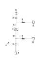
【解決手段】スイッチ装置60は、第1のゲート(80)を有し、第1の端子(64)と第2の端子(66)との間に結合された第1のトランジスタ(62)と、第2のゲート(82)を有し、第2の端子と第3の端子(70)との間に結合された第2のトランジスタ(68)と、インピーダンス部品(78)とを備える。第1、第2のトランジスタが、第1、第3の端子間において信号電流を導通するように構成され、インピーダンス部品は、信号電流の歪みを減少するために第1、第2のゲートに結合されている。
【選択図】図3
Description
VD1S1-DC=0
VD2S2-DC=0
VD2G2+VG2S2=VD2S2
VG1D1=VG1D1−DC+βVD1S1、その際、βは定数
VG2S2=VG2S2−DC+αVD2S2
VG2D2=VG2D2−DC+βVD2S2
VD1S1=−VD2S2
VG1D1=VDC+βVD1S1
VG2S2=VDC−αVD1S1
VG2D2=VDC−βVD1S1
RD2S2=AVG2S2+BVG2D2
=(A+B)VDC
第1のゲート(80)を有し、第1の端子(64)と第2の端子(66)との間に結合された第1のトランジスタ(62)と、第2のゲート(82)を有し、前記第2の端子と第3の端子(70)との間に結合された第2のトランジスタ(68)と、インピーダンス部品(78/178)とを備え、
前記第1のトランジスタ及び前記第2のトランジスタが、前記第1の端子と前記第3の端子との間において信号電流を導通するように構成され、前記インピーダンス部品(78/178)は、前記信号電流の歪みを減少するために、前記第1のゲートにおける第1のゲート信号電圧を絶縁し又は前記第2のゲートにおける第2のゲート信号電圧を絶縁するように構成された前記第1のゲート及び前記第2のゲートに結合されているスイッチ装置(60/160)。
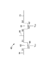
前記インピーダンス部品は、前記第1のゲートと第4の端子(86)との間に結合され前記第1のゲートにバイアス電圧を供給するための第1の抵抗(74)と、前記第2のゲートと前記第4の端子との間に結合され前記第2のゲートに前記バイアス電圧を供給する第2の抵抗とを備え、前記バイアス電圧が、前記第1のトランジスタ及び前記第2のトランジスタを不導通状態から導通状態に切り換えるために、前記第2の端子に対して相対的に十分であることを特徴とする、実施態様1に記載のスイッチ装置。
前記第1のゲートと前記第1の端子又は第2の端子との間のインピーダンスに対する第1の抵抗の抵抗値の比が、1より大きいことを特徴とする、実施態様2に記載のスイッチ装置。
前記第1のゲート信号電圧が第1の端子電圧と第2の端子電圧との間のほぼ中間にある値を有することを可能にするために、前記比が十分であることを特徴とする実施態様3に記載のスイッチ装置。
前記第1のトランジスタ及び前記第2のトランジスタが、実質的に整合した電気的特性を有し、前記第1の端子電圧と前記第2の端子電圧との間の差が、実質的に第3の端子電圧と前記第2の端子電圧との間の差に対して同じであり、及び極性について逆であるように、前記第1の抵抗及び前記第2の抵抗が、実質的に同じ値を有する、ことを特徴とする、実施態様4に記載のスイッチ装置。
前記第1のゲート信号電圧及び前記第2のゲート信号電圧が、等しくないことを特徴とする、実施態様2に記載のスイッチ装置。
前記第1、第2のトランジスタが、電界効果トランジスタであることを特徴とする、実施態様1に記載のスイッチ装置。
第1のゲート(80)を有し、第1の端子(64)と第2の端子(66)との間に結合された第1のトランジスタ(62)を備え、第2のゲート(82)を有し、前記第2の端子と第3の端子(70)との間に結合された第2のトランジスタ(68)を備え、前記第1の端子と前記第3の端子との間において信号電流を導通し、及び、前記信号電流の歪みを減少するために、前記第1のゲートにおける第1のゲート信号電圧、又は前記第2のゲートにおける第2のゲート信号電圧を絶縁することを有する、スイッチ装置(60/160)における信号電流を制御するための電流制御方法。
前記第1のゲート信号電圧が第1の端子電圧と第2の端子電圧との間のほぼ中間にある値を有することを可能にするために十分なインピーダンスを、第4の端子(86/118)と前記第1のゲートとの間に供給することを有する、実施態様8に記載の方法。
前記第2のゲート信号電圧が第2の端子電圧と第3の端子電圧との間のほぼ中間にある値を有することを可能にするために十分なインピーダンスを、第4の端子(86/118)と前記第2のゲートとの間に供給することを有する、実施態様8に記載の方法。
62 第1のトランジスタ
64 第1の端子
66 第2の端子
68 第2のトランジスタ
70 第3の端子
74 第1の抵抗
76 第2の抵抗
78 インピーダンス部品
80 第1のゲート
82 第2のゲート
86 第4の端子
118 第4の端子
160 スイッチ装置
178 インピーダンス部品
Claims (1)
- 第1のゲートを有し、第1の端子と第2の端子との間に結合された第1のトランジスタと、
第2のゲートを有し、前記第2の端子と第3の端子との間に結合された第2のトランジスタと、
インピーダンス部品とを備え、
前記第1のトランジスタ及び前記第2のトランジスタが、前記第1の端子と前記第3の端子との間において信号電流を導通するように構成され、前記インピーダンス部品は、前記信号電流の歪みを減少するために、前記第1のゲートにおける第1のゲート信号電圧を絶縁し又は前記第2のゲートにおける第2のゲート信号電圧を絶縁するように構成された前記第1のゲート及び前記第2のゲートに結合されているスイッチ装置。
Applications Claiming Priority (1)
| Application Number | Priority Date | Filing Date | Title |
|---|---|---|---|
| US10/261,711 US6900711B2 (en) | 2002-09-30 | 2002-09-30 | Switching system |
Publications (2)
| Publication Number | Publication Date |
|---|---|
| JP2004129251A true JP2004129251A (ja) | 2004-04-22 |
| JP2004129251A5 JP2004129251A5 (ja) | 2006-10-12 |
Family
ID=29401093
Family Applications (1)
| Application Number | Title | Priority Date | Filing Date |
|---|---|---|---|
| JP2003324983A Withdrawn JP2004129251A (ja) | 2002-09-30 | 2003-09-17 | スイッチ装置 |
Country Status (3)
| Country | Link |
|---|---|
| US (1) | US6900711B2 (ja) |
| JP (1) | JP2004129251A (ja) |
| GB (1) | GB2394610B (ja) |
Families Citing this family (10)
| Publication number | Priority date | Publication date | Assignee | Title |
|---|---|---|---|---|
| US7113744B1 (en) * | 1999-10-21 | 2006-09-26 | Broadcom Corporation | Adaptive radio transceiver with a power amplifier |
| US7177619B2 (en) * | 2005-01-25 | 2007-02-13 | International Business Machines Corporation | Dual gate FinFET radio frequency switch and mixer |
| US7982243B1 (en) | 2006-05-05 | 2011-07-19 | Rf Micro Devices, Inc. | Multiple gate transistor architecture providing an accessible inner source-drain node |
| US7459988B1 (en) * | 2006-09-18 | 2008-12-02 | Rf Micro Devices, Inc. | High linearity wide dynamic range radio frequency antenna switch |
| US20090085579A1 (en) * | 2007-09-28 | 2009-04-02 | Advantest Corporation | Attenuation apparatus and test apparatus |
| US7710148B2 (en) * | 2008-06-02 | 2010-05-04 | Suvolta, Inc. | Programmable switch circuit and method, method of manufacture, and devices and systems including the same |
| CN105453431B (zh) * | 2013-06-25 | 2017-12-12 | Ess技术有限公司 | 独立于电源电压的延时电路 |
| US11323147B1 (en) * | 2021-06-07 | 2022-05-03 | Futurecom Systems Group, ULC | Reducing insertion loss in a switch for a communication device |
| US12095496B2 (en) | 2021-10-18 | 2024-09-17 | Futurecom Systems Group, ULC | Self-diagnostic systems and method for a transceiver |
| US12041533B2 (en) | 2022-05-10 | 2024-07-16 | Motorola Solutions, Inc. | System and method for configuring a portable communication system |
Family Cites Families (25)
| Publication number | Priority date | Publication date | Assignee | Title |
|---|---|---|---|---|
| DE2851789C2 (de) * | 1978-11-30 | 1981-10-01 | Licentia Patent-Verwaltungs-Gmbh, 6000 Frankfurt | Schaltung zum Schalten und Übertragen von Wechselspannungen |
| US4417157A (en) | 1979-09-11 | 1983-11-22 | E-Systems, Inc. | Radio frequency switch for coupling an RF source to a load |
| IL68659A0 (en) | 1983-05-11 | 1983-09-30 | Tadiran Israel Elect Ind Ltd | Rf power switches |
| US4978932A (en) * | 1988-07-07 | 1990-12-18 | Communications Satellite Corporation | Microwave digitally controlled solid-state attenuator having parallel switched paths |
| US5012123A (en) | 1989-03-29 | 1991-04-30 | Hittite Microwave, Inc. | High-power rf switching system |
| US5027007A (en) * | 1989-04-12 | 1991-06-25 | The Boeing Company | FFL/QFL FET logic circuits |
| US5107152A (en) | 1989-09-08 | 1992-04-21 | Mia-Com, Inc. | Control component for a three-electrode device |
| US5350957A (en) * | 1989-10-20 | 1994-09-27 | Texas Instrument Incorporated | Electronic switch controlled by plural inputs |
| US5513390A (en) | 1991-03-12 | 1996-04-30 | Watkins Johnson Company | Biased FET mixer |
| US6064872A (en) | 1991-03-12 | 2000-05-16 | Watkins-Johnson Company | Totem pole mixer having grounded serially connected stacked FET pair |
| US5361409A (en) | 1991-03-12 | 1994-11-01 | Watkins Johnson Company | FET mixer having transmission line transformer |
| WO1995034913A1 (en) * | 1994-06-16 | 1995-12-21 | Anadigics, Inc. | Bootstrapped-gate field effect transistors and circuits thereof |
| US5678226A (en) | 1994-11-03 | 1997-10-14 | Watkins Johnson Company | Unbalanced FET mixer |
| JPH08204530A (ja) * | 1995-01-23 | 1996-08-09 | Sony Corp | スイツチ回路 |
| JPH0927736A (ja) | 1995-07-13 | 1997-01-28 | Japan Radio Co Ltd | Fetスイッチ |
| US5799248A (en) | 1995-12-20 | 1998-08-25 | Watkins-Johnson Company | Quasi-double balanced passive reflection FET mixer |
| US5697092A (en) | 1995-12-21 | 1997-12-09 | The Whitaker Corporation | Floating fet mixer |
| US5789995A (en) | 1996-09-20 | 1998-08-04 | Motorola, Inc. | Low loss electronic radio frequency switch |
| US5786722A (en) | 1996-11-12 | 1998-07-28 | Xerox Corporation | Integrated RF switching cell built in CMOS technology and utilizing a high voltage integrated circuit diode with a charge injecting node |
| JPH10242829A (ja) | 1997-02-24 | 1998-09-11 | Sanyo Electric Co Ltd | スイッチ回路装置 |
| JP2964975B2 (ja) | 1997-02-26 | 1999-10-18 | 日本電気株式会社 | 高周波スイッチ回路 |
| EP0875991A1 (de) * | 1997-04-25 | 1998-11-04 | Philips Patentverwaltung GmbH | Schaltungsanordnung zur Generierung eines elektronisch gesteuerten Widerstandes |
| US5990580A (en) * | 1998-03-05 | 1999-11-23 | The Whitaker Corporation | Single pole double throw switch |
| WO2001067602A2 (en) * | 2000-03-03 | 2001-09-13 | Alpha Industries, Inc. | Electronic switch |
| US6310508B1 (en) * | 2000-08-24 | 2001-10-30 | Agilent Technologies, Inc. | High frequency switch |
-
2002
- 2002-09-30 US US10/261,711 patent/US6900711B2/en not_active Expired - Fee Related
-
2003
- 2003-09-17 JP JP2003324983A patent/JP2004129251A/ja not_active Withdrawn
- 2003-09-26 GB GB0322616A patent/GB2394610B/en not_active Expired - Fee Related
Also Published As
| Publication number | Publication date |
|---|---|
| US6900711B2 (en) | 2005-05-31 |
| GB2394610B (en) | 2006-07-26 |
| GB2394610A (en) | 2004-04-28 |
| US20040061578A1 (en) | 2004-04-01 |
| GB0322616D0 (en) | 2003-10-29 |
Similar Documents
| Publication | Publication Date | Title |
|---|---|---|
| JP3902111B2 (ja) | スイッチ半導体集積回路 | |
| US7250804B2 (en) | Series/shunt switch and method of control | |
| US5945867A (en) | Switch circuit device | |
| US6154085A (en) | Constant gate drive MOS analog switch | |
| US5767721A (en) | Switch circuit for FET devices having negative threshold voltages which utilize a positive voltage only | |
| US8283808B2 (en) | Switch arrangement and method for electrical switching | |
| US10523197B2 (en) | Switch circuit, corresponding device and method | |
| US20050161700A1 (en) | Integrated power switching circuit | |
| US7852172B2 (en) | High-power switch | |
| JP2004129251A (ja) | スイッチ装置 | |
| US11646733B2 (en) | Digital output driver circuit and method | |
| US6498533B1 (en) | Bootstrapped dual-gate class E amplifier circuit | |
| JP4828343B2 (ja) | アナログスイッチ回路 | |
| CN100405739C (zh) | 串联/分路开关及操作方法 | |
| JP7357562B2 (ja) | 高周波スイッチ回路 | |
| JP3539106B2 (ja) | 高周波用半導体スイッチ回路およびそれを用いた制御方法 | |
| JP7425623B2 (ja) | 高周波スイッチ回路 | |
| JP2008283277A (ja) | 半導体スイッチ回路 | |
| US4551644A (en) | Field effect transistor gate circuit for analog signals | |
| JP2761555B2 (ja) | 周波数変換器 | |
| JP3657382B2 (ja) | 増幅用トランジスタの動作状態を切り換えるオートバイアス回路 | |
| JP2002314393A (ja) | 低しきい値mosトランジスタの電源スタンバイ回路 | |
| KR20020036873A (ko) | 상보형 금속 산화물 반도체 집적 회로상에 구현되는저항기 회로 및 그 회로 구현 방법 | |
| JPS6161520A (ja) | 高周波信号スイツチ回路 |
Legal Events
| Date | Code | Title | Description |
|---|---|---|---|
| A521 | Request for written amendment filed |
Free format text: JAPANESE INTERMEDIATE CODE: A523 Effective date: 20060824 |
|
| A621 | Written request for application examination |
Free format text: JAPANESE INTERMEDIATE CODE: A621 Effective date: 20060824 |
|
| A711 | Notification of change in applicant |
Free format text: JAPANESE INTERMEDIATE CODE: A711 Effective date: 20070328 |
|
| RD03 | Notification of appointment of power of attorney |
Free format text: JAPANESE INTERMEDIATE CODE: A7423 Effective date: 20070409 |
|
| A761 | Written withdrawal of application |
Free format text: JAPANESE INTERMEDIATE CODE: A761 Effective date: 20070501 |