JP2004239925A - 電子回路検査装置 - Google Patents
電子回路検査装置 Download PDFInfo
- Publication number
- JP2004239925A JP2004239925A JP2004159754A JP2004159754A JP2004239925A JP 2004239925 A JP2004239925 A JP 2004239925A JP 2004159754 A JP2004159754 A JP 2004159754A JP 2004159754 A JP2004159754 A JP 2004159754A JP 2004239925 A JP2004239925 A JP 2004239925A
- Authority
- JP
- Japan
- Prior art keywords
- circuit
- waveform
- under test
- inspection
- signal
- Prior art date
- Legal status (The legal status is an assumption and is not a legal conclusion. Google has not performed a legal analysis and makes no representation as to the accuracy of the status listed.)
- Granted
Links
Images


Landscapes
- Tests Of Electronic Circuits (AREA)
- Testing Of Individual Semiconductor Devices (AREA)
Abstract
さらに、汎用性のある電子回路検査装置を提供する。
【解決手段】 被検査回路にパルス信号を印加するパルス信号源15と、前記被検査回路の前記パルス信号に対する過渡応答信号をアナログデジタル変換するアナログデジタル変換器11と、前記デジタル変換された過渡応答信号を演算処理し、過渡応答信号波形の包絡線が、正常回路の応答波形にもとづいて予め設定した範囲内にあるかどうかにより、前記被検査回路の異常を判定するマイクロプロセッサ12と、前記被検査回路の検査結果を表示する表示装置14とで電子回路検査装置10を構成する。
【選択図】 図1
Description
また、被検査回路の異常によって一般的に発生する変化を指標として異常を判定しているので、汎用性のある電子回路検査装置が提供できる。
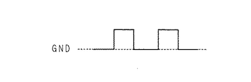
図1は本発明の実施の形態1における自動電子回路検査装置の計測回路図、図2はパルス信号源15から出力されるステップ信号波形を示す図、図3はパルス信号源15から出力される矩形波信号波形を示す図、図4および図5はトランス3の2次側3bで測定される出力過渡応答波形を示す図である。図1に示す被検査回路は、具体的にはチョークコイル電流制御型一石自励インバータ回路のうち、本発明の検査方法に関連する電子回路素子を抜粋したものである。パルス信号源15は、検査を行うために被検査回路にパルス信号を供給するためのもので、被検査回路の過渡応答は、トランス2次側3bの両端から電圧波形変化として測定するものである。
本実施の形態は、マイクロプロセッサ12による過渡応答波形の演算処理と判定の具体的方法を説明するものである。実施の形態1にあげたダイオードの接続不良の例では、正常波形と異常波形の違いが主として振動波形の継続時間の違いとして現れる。このような場合には、過渡応答波形の実効値あるいは整流値を積分し、その積分値の大小によって振動波形の継続時間の違いを判定する方法が適している。また、実効値回路、整流回路、積分回路等のアナログ演算処理回路をアナログデジタル変換器11の前に設けて、マイクロプロセッサ12による演算の替りにアナログ信号処理として行うようにすれば、マイクロプロセッサ12の演算処理を軽減することができ、判定処理時間を短縮することができる。また、マイクロプロセッサによる演算処理に比べて、より高速な応答波形の演算処理が可能となる。
Claims (1)
- 被検査回路にパルス信号を印加するパルス信号源と、前記被検査回路の前記パルス信号に対する過渡応答信号をアナログデジタル変換するアナログデジタル変換器と、前記デジタル変換された過渡応答信号を演算処理し、過渡応答信号波形の包絡線が、正常回路の応答波形にもとづいて予め設定した範囲内にあるかどうかにより、前記被検査回路の異常を判定するマイクロプロセッサと、前記被検査回路の検査結果を表示する表示装置とを備えた電子回路検査装置。
Priority Applications (1)
| Application Number | Priority Date | Filing Date | Title |
|---|---|---|---|
| JP2004159754A JP3818299B2 (ja) | 1997-09-30 | 2004-05-28 | 電子回路検査装置 |
Applications Claiming Priority (2)
| Application Number | Priority Date | Filing Date | Title |
|---|---|---|---|
| JP26682797A JP3577912B2 (ja) | 1997-09-30 | 1997-09-30 | 電子回路検査装置 |
| JP2004159754A JP3818299B2 (ja) | 1997-09-30 | 2004-05-28 | 電子回路検査装置 |
Related Parent Applications (1)
| Application Number | Title | Priority Date | Filing Date |
|---|---|---|---|
| JP26682797A Division JP3577912B2 (ja) | 1997-09-30 | 1997-09-30 | 電子回路検査装置 |
Publications (2)
| Publication Number | Publication Date |
|---|---|
| JP2004239925A true JP2004239925A (ja) | 2004-08-26 |
| JP3818299B2 JP3818299B2 (ja) | 2006-09-06 |
Family
ID=17436212
Family Applications (3)
| Application Number | Title | Priority Date | Filing Date |
|---|---|---|---|
| JP26682797A Expired - Fee Related JP3577912B2 (ja) | 1997-09-30 | 1997-09-30 | 電子回路検査装置 |
| JP2004159754A Expired - Fee Related JP3818299B2 (ja) | 1997-09-30 | 2004-05-28 | 電子回路検査装置 |
| JP2004159755A Expired - Fee Related JP3856013B2 (ja) | 1997-09-30 | 2004-05-28 | 電子回路検査装置 |
Family Applications Before (1)
| Application Number | Title | Priority Date | Filing Date |
|---|---|---|---|
| JP26682797A Expired - Fee Related JP3577912B2 (ja) | 1997-09-30 | 1997-09-30 | 電子回路検査装置 |
Family Applications After (1)
| Application Number | Title | Priority Date | Filing Date |
|---|---|---|---|
| JP2004159755A Expired - Fee Related JP3856013B2 (ja) | 1997-09-30 | 2004-05-28 | 電子回路検査装置 |
Country Status (1)
| Country | Link |
|---|---|
| JP (3) | JP3577912B2 (ja) |
Cited By (1)
| Publication number | Priority date | Publication date | Assignee | Title |
|---|---|---|---|---|
| CN108693464A (zh) * | 2017-04-01 | 2018-10-23 | 亚德诺半导体集团 | 用于故障检测的模拟输入电路传感 |
Families Citing this family (3)
| Publication number | Priority date | Publication date | Assignee | Title |
|---|---|---|---|---|
| JP2001264398A (ja) * | 1999-11-22 | 2001-09-26 | Fujitsu Ten Ltd | 電子部品検査装置及び検査方法 |
| JP4596834B2 (ja) * | 2004-07-07 | 2010-12-15 | 日置電機株式会社 | 電子回路検査装置および電子回路検査方法 |
| KR101913385B1 (ko) * | 2015-05-08 | 2018-10-30 | 전자부품연구원 | 반도체 소자 진단장치 |
Family Cites Families (4)
| Publication number | Priority date | Publication date | Assignee | Title |
|---|---|---|---|---|
| JPS56155862A (en) * | 1980-05-07 | 1981-12-02 | Komatsu Ltd | Frequency measuring method |
| JPS5879169A (ja) * | 1981-11-05 | 1983-05-12 | Nippon Telegr & Teleph Corp <Ntt> | 半導体素子評価法 |
| JPS608760A (ja) * | 1983-06-29 | 1985-01-17 | Yuniki Eng:Kk | 各種コイルの判定装置 |
| JPS63200079A (ja) * | 1987-02-16 | 1988-08-18 | Canon Inc | 半導体素子の特性測定方式 |
-
1997
- 1997-09-30 JP JP26682797A patent/JP3577912B2/ja not_active Expired - Fee Related
-
2004
- 2004-05-28 JP JP2004159754A patent/JP3818299B2/ja not_active Expired - Fee Related
- 2004-05-28 JP JP2004159755A patent/JP3856013B2/ja not_active Expired - Fee Related
Cited By (2)
| Publication number | Priority date | Publication date | Assignee | Title |
|---|---|---|---|---|
| CN108693464A (zh) * | 2017-04-01 | 2018-10-23 | 亚德诺半导体集团 | 用于故障检测的模拟输入电路传感 |
| US10852360B2 (en) | 2017-04-01 | 2020-12-01 | Analog Devices International Unlimited Company | ADC input circuit sensing for fault detection |
Also Published As
| Publication number | Publication date |
|---|---|
| JPH11108997A (ja) | 1999-04-23 |
| JP3818299B2 (ja) | 2006-09-06 |
| JP2004271538A (ja) | 2004-09-30 |
| JP3577912B2 (ja) | 2004-10-20 |
| JP3856013B2 (ja) | 2006-12-13 |
Similar Documents
| Publication | Publication Date | Title |
|---|---|---|
| JPH06160457A (ja) | 回路板試験装置 | |
| JPH07191080A (ja) | 電気接続の完全性を測定するための装置と方法 | |
| US10139454B2 (en) | Test device and alternating current power detection method of the same | |
| JP3577912B2 (ja) | 電子回路検査装置 | |
| US20010028256A1 (en) | Diagnostic apparatus for electronics circuit and diagnostic method using same | |
| US20040095124A1 (en) | Automatic multimeter | |
| JP3784479B2 (ja) | 回路基板検査方法 | |
| JP4259692B2 (ja) | 回路基板検査装置 | |
| JPH1026647A (ja) | 基板検査方法及び装置 | |
| JPS62187258A (ja) | 回路板の検査方法 | |
| JPH1164428A (ja) | 部品検査装置 | |
| JP3241777B2 (ja) | インサーキットテスタ用オープンテスト装置 | |
| JP2730504B2 (ja) | 試験用プローブピンの接触不良判断方法およびインサーキットテスタ | |
| KR100188693B1 (ko) | 반도체칩의 리드 오픈 검사 장치 | |
| JP2007155640A (ja) | 集積回路の検査方法と検査装置 | |
| US20170205449A1 (en) | Test device and alternating current power detection method of the same | |
| JPH04315068A (ja) | プリント回路板の検査装置 | |
| JPH11183529A (ja) | 微小電流測定方法および微小電流測定装置 | |
| JPH05264676A (ja) | 故障検出方法及び検出装置 | |
| KR100215510B1 (ko) | Pcb자동측정검사장치에서의 핀접촉검사방법 및 그장치 | |
| JP2002057454A (ja) | 集積回路の接合状態判定方法、及び集積回路の接合状態検査装置 | |
| JP3271605B2 (ja) | プリント基板の半田付け不良検出装置 | |
| JPH0541419A (ja) | 検査装置の評価方法 | |
| JPH1114703A (ja) | 電子回路基板における不良個所特定装置 | |
| JPS5856834B2 (ja) | 接触状態検知方法 |
Legal Events
| Date | Code | Title | Description |
|---|---|---|---|
| A621 | Written request for application examination |
Free format text: JAPANESE INTERMEDIATE CODE: A621 Effective date: 20040528 |
|
| A977 | Report on retrieval |
Free format text: JAPANESE INTERMEDIATE CODE: A971007 Effective date: 20060217 |
|
| TRDD | Decision of grant or rejection written | ||
| A01 | Written decision to grant a patent or to grant a registration (utility model) |
Free format text: JAPANESE INTERMEDIATE CODE: A01 Effective date: 20060523 |
|
| A61 | First payment of annual fees (during grant procedure) |
Free format text: JAPANESE INTERMEDIATE CODE: A61 Effective date: 20060605 |
|
| FPAY | Renewal fee payment (event date is renewal date of database) |
Free format text: PAYMENT UNTIL: 20100623 Year of fee payment: 4 |
|
| FPAY | Renewal fee payment (event date is renewal date of database) |
Free format text: PAYMENT UNTIL: 20100623 Year of fee payment: 4 |
|
| FPAY | Renewal fee payment (event date is renewal date of database) |
Free format text: PAYMENT UNTIL: 20110623 Year of fee payment: 5 |
|
| FPAY | Renewal fee payment (event date is renewal date of database) |
Free format text: PAYMENT UNTIL: 20120623 Year of fee payment: 6 |
|
| FPAY | Renewal fee payment (event date is renewal date of database) |
Free format text: PAYMENT UNTIL: 20130623 Year of fee payment: 7 |
|
| LAPS | Cancellation because of no payment of annual fees |