JP2004247735A - 選択的エピタキシャル成長を利用した半導体素子の局部配線形成方法 - Google Patents
選択的エピタキシャル成長を利用した半導体素子の局部配線形成方法 Download PDFInfo
- Publication number
- JP2004247735A JP2004247735A JP2004034272A JP2004034272A JP2004247735A JP 2004247735 A JP2004247735 A JP 2004247735A JP 2004034272 A JP2004034272 A JP 2004034272A JP 2004034272 A JP2004034272 A JP 2004034272A JP 2004247735 A JP2004247735 A JP 2004247735A
- Authority
- JP
- Japan
- Prior art keywords
- selective epitaxial
- forming
- epitaxial growth
- local wiring
- gate
- Prior art date
- Legal status (The legal status is an assumption and is not a legal conclusion. Google has not performed a legal analysis and makes no representation as to the accuracy of the status listed.)
- Pending
Links
Images


Classifications
-
- H—ELECTRICITY
- H10—SEMICONDUCTOR DEVICES; ELECTRIC SOLID-STATE DEVICES NOT OTHERWISE PROVIDED FOR
- H10D—INORGANIC ELECTRIC SEMICONDUCTOR DEVICES
- H10D64/00—Electrodes of devices having potential barriers
- H10D64/01—Manufacture or treatment
- H10D64/011—Manufacture or treatment of electrodes ohmically coupled to a semiconductor
-
- H—ELECTRICITY
- H10—SEMICONDUCTOR DEVICES; ELECTRIC SOLID-STATE DEVICES NOT OTHERWISE PROVIDED FOR
- H10W—GENERIC PACKAGES, INTERCONNECTIONS, CONNECTORS OR OTHER CONSTRUCTIONAL DETAILS OF DEVICES COVERED BY CLASS H10
- H10W20/00—Interconnections in chips, wafers or substrates
- H10W20/01—Manufacture or treatment
- H10W20/031—Manufacture or treatment of conductive parts of the interconnections
- H10W20/0698—Local interconnections
-
- H—ELECTRICITY
- H10—SEMICONDUCTOR DEVICES; ELECTRIC SOLID-STATE DEVICES NOT OTHERWISE PROVIDED FOR
- H10D—INORGANIC ELECTRIC SEMICONDUCTOR DEVICES
- H10D64/00—Electrodes of devices having potential barriers
- H10D64/01—Manufacture or treatment
- H10D64/011—Manufacture or treatment of electrodes ohmically coupled to a semiconductor
- H10D64/0111—Manufacture or treatment of electrodes ohmically coupled to a semiconductor to Group IV semiconductors
- H10D64/0112—Manufacture or treatment of electrodes ohmically coupled to a semiconductor to Group IV semiconductors using conductive layers comprising silicides
-
- H—ELECTRICITY
- H10—SEMICONDUCTOR DEVICES; ELECTRIC SOLID-STATE DEVICES NOT OTHERWISE PROVIDED FOR
- H10D—INORGANIC ELECTRIC SEMICONDUCTOR DEVICES
- H10D84/00—Integrated devices formed in or on semiconductor substrates that comprise only semiconducting layers, e.g. on Si wafers or on GaAs-on-Si wafers
- H10D84/01—Manufacture or treatment
- H10D84/0123—Integrating together multiple components covered by H10D12/00 or H10D30/00, e.g. integrating multiple IGBTs
- H10D84/0126—Integrating together multiple components covered by H10D12/00 or H10D30/00, e.g. integrating multiple IGBTs the components including insulated gates, e.g. IGFETs
- H10D84/0165—Integrating together multiple components covered by H10D12/00 or H10D30/00, e.g. integrating multiple IGBTs the components including insulated gates, e.g. IGFETs the components including complementary IGFETs, e.g. CMOS devices
- H10D84/0186—Manufacturing their interconnections or electrodes, e.g. source or drain electrodes
-
- H—ELECTRICITY
- H10—SEMICONDUCTOR DEVICES; ELECTRIC SOLID-STATE DEVICES NOT OTHERWISE PROVIDED FOR
- H10D—INORGANIC ELECTRIC SEMICONDUCTOR DEVICES
- H10D84/00—Integrated devices formed in or on semiconductor substrates that comprise only semiconducting layers, e.g. on Si wafers or on GaAs-on-Si wafers
- H10D84/01—Manufacture or treatment
- H10D84/02—Manufacture or treatment characterised by using material-based technologies
- H10D84/03—Manufacture or treatment characterised by using material-based technologies using Group IV technology, e.g. silicon technology or silicon-carbide [SiC] technology
- H10D84/038—Manufacture or treatment characterised by using material-based technologies using Group IV technology, e.g. silicon technology or silicon-carbide [SiC] technology using silicon technology, e.g. SiGe
-
- H—ELECTRICITY
- H10—SEMICONDUCTOR DEVICES; ELECTRIC SOLID-STATE DEVICES NOT OTHERWISE PROVIDED FOR
- H10P—GENERIC PROCESSES OR APPARATUS FOR THE MANUFACTURE OR TREATMENT OF DEVICES COVERED BY CLASS H10
- H10P14/00—Formation of materials, e.g. in the shape of layers or pillars
- H10P14/20—Formation of materials, e.g. in the shape of layers or pillars of semiconductor materials
- H10P14/24—Formation of materials, e.g. in the shape of layers or pillars of semiconductor materials using chemical vapour deposition [CVD]
-
- H—ELECTRICITY
- H10—SEMICONDUCTOR DEVICES; ELECTRIC SOLID-STATE DEVICES NOT OTHERWISE PROVIDED FOR
- H10P—GENERIC PROCESSES OR APPARATUS FOR THE MANUFACTURE OR TREATMENT OF DEVICES COVERED BY CLASS H10
- H10P14/00—Formation of materials, e.g. in the shape of layers or pillars
- H10P14/20—Formation of materials, e.g. in the shape of layers or pillars of semiconductor materials
- H10P14/27—Formation of materials, e.g. in the shape of layers or pillars of semiconductor materials using selective deposition, e.g. simultaneous growth of monocrystalline and non-monocrystalline semiconductor materials
- H10P14/271—Formation of materials, e.g. in the shape of layers or pillars of semiconductor materials using selective deposition, e.g. simultaneous growth of monocrystalline and non-monocrystalline semiconductor materials characterised by the preparation of substrate for selective deposition
-
- H—ELECTRICITY
- H10—SEMICONDUCTOR DEVICES; ELECTRIC SOLID-STATE DEVICES NOT OTHERWISE PROVIDED FOR
- H10P—GENERIC PROCESSES OR APPARATUS FOR THE MANUFACTURE OR TREATMENT OF DEVICES COVERED BY CLASS H10
- H10P14/00—Formation of materials, e.g. in the shape of layers or pillars
- H10P14/20—Formation of materials, e.g. in the shape of layers or pillars of semiconductor materials
- H10P14/27—Formation of materials, e.g. in the shape of layers or pillars of semiconductor materials using selective deposition, e.g. simultaneous growth of monocrystalline and non-monocrystalline semiconductor materials
- H10P14/271—Formation of materials, e.g. in the shape of layers or pillars of semiconductor materials using selective deposition, e.g. simultaneous growth of monocrystalline and non-monocrystalline semiconductor materials characterised by the preparation of substrate for selective deposition
- H10P14/274—Formation of materials, e.g. in the shape of layers or pillars of semiconductor materials using selective deposition, e.g. simultaneous growth of monocrystalline and non-monocrystalline semiconductor materials characterised by the preparation of substrate for selective deposition using seed materials
-
- H—ELECTRICITY
- H10—SEMICONDUCTOR DEVICES; ELECTRIC SOLID-STATE DEVICES NOT OTHERWISE PROVIDED FOR
- H10P—GENERIC PROCESSES OR APPARATUS FOR THE MANUFACTURE OR TREATMENT OF DEVICES COVERED BY CLASS H10
- H10P14/00—Formation of materials, e.g. in the shape of layers or pillars
- H10P14/20—Formation of materials, e.g. in the shape of layers or pillars of semiconductor materials
- H10P14/29—Formation of materials, e.g. in the shape of layers or pillars of semiconductor materials characterised by the substrates
- H10P14/2901—Materials
- H10P14/2902—Materials being Group IVA materials
- H10P14/2905—Silicon, silicon germanium or germanium
-
- H—ELECTRICITY
- H10—SEMICONDUCTOR DEVICES; ELECTRIC SOLID-STATE DEVICES NOT OTHERWISE PROVIDED FOR
- H10P—GENERIC PROCESSES OR APPARATUS FOR THE MANUFACTURE OR TREATMENT OF DEVICES COVERED BY CLASS H10
- H10P14/00—Formation of materials, e.g. in the shape of layers or pillars
- H10P14/20—Formation of materials, e.g. in the shape of layers or pillars of semiconductor materials
- H10P14/34—Deposited materials, e.g. layers
- H10P14/3402—Deposited materials, e.g. layers characterised by the chemical composition
- H10P14/3404—Deposited materials, e.g. layers characterised by the chemical composition being Group IVA materials
- H10P14/3411—Silicon, silicon germanium or germanium
-
- H—ELECTRICITY
- H10—SEMICONDUCTOR DEVICES; ELECTRIC SOLID-STATE DEVICES NOT OTHERWISE PROVIDED FOR
- H10P—GENERIC PROCESSES OR APPARATUS FOR THE MANUFACTURE OR TREATMENT OF DEVICES COVERED BY CLASS H10
- H10P14/00—Formation of materials, e.g. in the shape of layers or pillars
- H10P14/20—Formation of materials, e.g. in the shape of layers or pillars of semiconductor materials
- H10P14/38—Formation of materials, e.g. in the shape of layers or pillars of semiconductor materials characterised by treatments done after the formation of the materials
Landscapes
- Insulated Gate Type Field-Effect Transistor (AREA)
- Internal Circuitry In Semiconductor Integrated Circuit Devices (AREA)
- Semiconductor Memories (AREA)
- Electrodes Of Semiconductors (AREA)
- Metal-Oxide And Bipolar Metal-Oxide Semiconductor Integrated Circuits (AREA)
- Recrystallisation Techniques (AREA)
Abstract
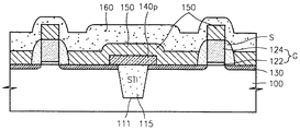
【解決手段】 局部配線が形成される半導体基板上の領域であって選択的エピタキシャル成長シード層(140)のない領域上に選択的エピタキシャル成長シード層パターン(140P)を形成した後、選択的エピタキシャル成長を実施し、形成された選択的エピタキシャル層(150)の抵抗を下げて局部配線を完成する。本発明により、単純かつ容易な工程で局部配線を形成できる。
【選択図】 図4
Description
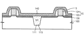
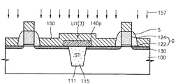
111 トレンチ
115 絶縁膜
122 ゲート酸化膜
124 ポリシリコン膜
G ゲート
130 LDD領域
140 選択的エピタキシャル成長シード層
150 選択的エピタキシャル層
155 イオン注入
S 絶縁スペーサ
STI トレンチ素子分離領域
Claims (8)
- 局部配線が形成される半導体基板上の領域であって選択的エピタキシャル成長シード層のない領域上に選択的エピタキシャル成長シード層パターンを形成する段階と、
前記結果物に対して選択的エピタキシャル成長を実施して選択的エピタキシャル層を形成する段階と、
前記選択的エピタキシャル層の抵抗を下げて前記局部配線として完成する段階と、を含むことを特徴とする局部配線を含む半導体素子の製造方法。 - 前記選択的エピタキシャル成長シード層パターンを形成する段階前に、
前記半導体基板に浅いトレンチ素子分離領域を形成して活性領域を定義する段階と、
前記活性領域上にそれぞれゲートを形成する段階と、
前記ゲート側壁にスペーサを形成する段階と、をさらに具備し、
前記選択的エピタキシャル成長シード層パターンを形成する段階は、
前記浅いトレンチ素子分離領域上に前記選択的エピタキシャル成長シード層パターンを形成する段階であり、
前記選択的エピタキシャル層を形成する段階は、
前記活性領域、前記選択的エピタキシャル成長シード層パターン、及び前記ゲート上に前記選択的エピタキシャル層を形成する段階であり、
前記局部配線はトランジスタのソース/ドレーンと隣接トランジスタのソース/ドレーンとを連結する局部配線であることを特徴とする請求項1に記載の局部配線を含む半導体素子の製造方法。 - 前記選択的エピタキシャル成長シード層パターンを形成する段階前に、
前記半導体基板に浅いトレンチ素子分離領域を形成して活性領域を定義する段階と、
前記活性領域上に相互隣接した第1及び第2ゲートを形成する段階と、
前記第1及び第2ゲート側壁にスペーサを形成する段階と、
前記第1ゲートが形成されている活性領域と前記第2ゲートとを露出させる絶縁膜パターンとを形成する段階と、をさらに具備し、
前記選択的エピタキシャル成長シード層パターンを形成する段階は、
前記絶縁膜パターン上に前記選択的エピタキシャル成長シード層パターンを形成する段階であり、
前記選択的エピタキシャル層を形成する段階は、
前記第1ゲートが形成されている活性領域、前記選択的エピタキシャル成長シード層パターン、及び前記第2ゲート上に前記選択的エピタキシャル層を形成する段階であり、
前記局部配線はトランジスタのソース/ドレーンと隣接トランジスタのゲートとを連結する局部配線であることを特徴とする請求項1に記載の局部配線を含む半導体素子の製造方法。 - 前記選択的エピタキシャル層の抵抗を下げて前記局部配線として完成する段階は、
前記選択的エピタキシャル層にイオンを注入して抵抗を下げる段階であることを特徴とする請求項1ないし請求項3のうち何れか1項に記載の局部配線を含む半導体素子の製造方法。 - 前記選択的エピタキシャル層の抵抗を下げて前記局部配線として完成する段階は、
前記選択的エピタキシャル層をシリサイド化して抵抗を下げる段階であることを特徴とする請求項1ないし請求項3のうち何れか1項に記載の局部配線を含む半導体素子の製造方法。 - 前記選択的エピタキシャル層の抵抗を下げて前記局部配線として完成する段階は、
前記選択的エピタキシャル層にイオンを注入する段階と、
前記選択的エピタキシャル層をシリサイド化する段階と、を含むことを特徴とする請求項1ないし請求項3のうち何れか1項に記載の局部配線を含む半導体素子の製造方法。 - 前記選択的エピタキシャル成長シード層パターンはSixOyNz層パターンであることを特徴とする請求項1ないし請求項3のうち何れか1項に記載の局部配線を含む半導体素子の製造方法。
- 前記選択的エピタキシャル成長シード層パターンはSixOyNz層パターンであり、xは55、yは15、zは30であることを特徴とする請求項7に記載の局部配線を含む半導体素子の製造方法。
Applications Claiming Priority (1)
| Application Number | Priority Date | Filing Date | Title |
|---|---|---|---|
| KR10-2003-0009139A KR100493047B1 (ko) | 2003-02-13 | 2003-02-13 | 선택적 에피택셜 성장을 이용한 반도체 소자의 국부 배선형성 방법 |
Publications (1)
| Publication Number | Publication Date |
|---|---|
| JP2004247735A true JP2004247735A (ja) | 2004-09-02 |
Family
ID=33028805
Family Applications (1)
| Application Number | Title | Priority Date | Filing Date |
|---|---|---|---|
| JP2004034272A Pending JP2004247735A (ja) | 2003-02-13 | 2004-02-10 | 選択的エピタキシャル成長を利用した半導体素子の局部配線形成方法 |
Country Status (3)
| Country | Link |
|---|---|
| US (1) | US7049218B2 (ja) |
| JP (1) | JP2004247735A (ja) |
| KR (1) | KR100493047B1 (ja) |
Cited By (3)
| Publication number | Priority date | Publication date | Assignee | Title |
|---|---|---|---|---|
| KR100653853B1 (ko) * | 2005-05-24 | 2006-12-05 | 네오폴리((주)) | 비금속 씨드 에피 성장을 이용한 비정질 반도체 박막의결정화 방법 및 이를 이용한 다결정 박막 트랜지스터의제조방법 |
| JP2013546158A (ja) * | 2010-09-06 | 2013-12-26 | ユ−ジーン テクノロジー カンパニー.リミテッド | 半導体素子の製造方法 |
| CN107017256A (zh) * | 2016-01-15 | 2017-08-04 | 台湾积体电路制造股份有限公司 | 半导体器件中的局部互连件及其制造方法 |
Families Citing this family (3)
| Publication number | Priority date | Publication date | Assignee | Title |
|---|---|---|---|---|
| CN102566090B (zh) | 2010-12-22 | 2014-12-10 | 李冰 | 一种光波导开关 |
| WO2012083862A1 (en) | 2010-12-22 | 2012-06-28 | Bing Li | Waveguide photodetector and forming method thereof |
| CN102565932B (zh) | 2011-01-14 | 2014-10-08 | 李冰 | 色散校正的阵列波导光栅 |
Citations (4)
| Publication number | Priority date | Publication date | Assignee | Title |
|---|---|---|---|---|
| JPH1187266A (ja) * | 1997-09-09 | 1999-03-30 | Oki Electric Ind Co Ltd | 半導体装置の製造方法 |
| JP2000114262A (ja) * | 1998-10-05 | 2000-04-21 | Toshiba Corp | 半導体装置及びその製造方法 |
| JP2001217319A (ja) * | 2000-02-04 | 2001-08-10 | Hitachi Ltd | 半導体集積回路装置およびその製造方法 |
| JP2003197768A (ja) * | 2001-12-25 | 2003-07-11 | Toshiba Corp | 半導体装置及びその製造方法 |
Family Cites Families (4)
| Publication number | Priority date | Publication date | Assignee | Title |
|---|---|---|---|---|
| US5166771A (en) * | 1990-01-12 | 1992-11-24 | Paradigm Technology, Inc. | Self-aligning contact and interconnect structure |
| US5118639A (en) * | 1990-05-29 | 1992-06-02 | Motorola, Inc. | Process for the formation of elevated source and drain structures in a semiconductor device |
| US5893741A (en) | 1997-02-07 | 1999-04-13 | National Science Council | Method for simultaneously forming local interconnect with silicided elevated source/drain MOSFET's |
| EP1280189A1 (en) * | 2001-07-16 | 2003-01-29 | Alcatel | Process for selective epitaxial growth and bipolar transistor made by using such process |
-
2003
- 2003-02-13 KR KR10-2003-0009139A patent/KR100493047B1/ko not_active Expired - Fee Related
-
2004
- 2004-01-28 US US10/766,645 patent/US7049218B2/en not_active Expired - Fee Related
- 2004-02-10 JP JP2004034272A patent/JP2004247735A/ja active Pending
Patent Citations (4)
| Publication number | Priority date | Publication date | Assignee | Title |
|---|---|---|---|---|
| JPH1187266A (ja) * | 1997-09-09 | 1999-03-30 | Oki Electric Ind Co Ltd | 半導体装置の製造方法 |
| JP2000114262A (ja) * | 1998-10-05 | 2000-04-21 | Toshiba Corp | 半導体装置及びその製造方法 |
| JP2001217319A (ja) * | 2000-02-04 | 2001-08-10 | Hitachi Ltd | 半導体集積回路装置およびその製造方法 |
| JP2003197768A (ja) * | 2001-12-25 | 2003-07-11 | Toshiba Corp | 半導体装置及びその製造方法 |
Cited By (6)
| Publication number | Priority date | Publication date | Assignee | Title |
|---|---|---|---|---|
| KR100653853B1 (ko) * | 2005-05-24 | 2006-12-05 | 네오폴리((주)) | 비금속 씨드 에피 성장을 이용한 비정질 반도체 박막의결정화 방법 및 이를 이용한 다결정 박막 트랜지스터의제조방법 |
| JP2013546158A (ja) * | 2010-09-06 | 2013-12-26 | ユ−ジーン テクノロジー カンパニー.リミテッド | 半導体素子の製造方法 |
| CN107017256A (zh) * | 2016-01-15 | 2017-08-04 | 台湾积体电路制造股份有限公司 | 半导体器件中的局部互连件及其制造方法 |
| KR101810319B1 (ko) * | 2016-01-15 | 2017-12-18 | 타이완 세미콘덕터 매뉴팩쳐링 컴퍼니 리미티드 | 반도체 디바이스 내에 국소 상호접속부를 제조하기 위한 방법 |
| US9881872B2 (en) | 2016-01-15 | 2018-01-30 | Taiwan Semiconductor Manufacturing Co., Ltd. | Method for fabricating a local interconnect in a semiconductor device |
| US10157845B2 (en) | 2016-01-15 | 2018-12-18 | Taiwan Semiconductor Manufacturing Co., Ltd. | Method for fabricating a local interconnect in a semiconductor device |
Also Published As
| Publication number | Publication date |
|---|---|
| US20040209454A1 (en) | 2004-10-21 |
| KR20040073154A (ko) | 2004-08-19 |
| KR100493047B1 (ko) | 2005-06-07 |
| US7049218B2 (en) | 2006-05-23 |
Similar Documents
| Publication | Publication Date | Title |
|---|---|---|
| US10840374B2 (en) | Semiconductor devices with shaped portions of elevated source/drain regions | |
| US20210313467A1 (en) | Semiconductor device including gate electrode for applying tensile stress to silicon substrate, and method of manufacturing the same | |
| US7666748B2 (en) | Method of forming amorphous source/drain extensions | |
| US5998849A (en) | Semiconductor device having highly-doped source/drain regions with interior edges in a dislocation-free state | |
| JP3731998B2 (ja) | 埋込型メモリ論理素子及びその製造方法 | |
| TW200939353A (en) | Method for fabricating super-steep retrograde well MOSFET on SOI or bulk silicon substrate, and device fabricated in accordance with the method | |
| JP2004214628A (ja) | Cmosデバイスおよびその製造方法 | |
| KR20100081667A (ko) | 스트레인드 채널을 갖는 반도체 장치 및 그 제조 방법 | |
| KR20060032662A (ko) | 집적형 금속 실리사이드 게이트 전극을 구비한트랜지스터의 형성 방법 | |
| JP2004527127A (ja) | Mosトランジスタ・ゲート・コーナの増速酸化を行う方法 | |
| CN101490836A (zh) | 用于数据存储电路的非对称性晶体管 | |
| KR100493047B1 (ko) | 선택적 에피택셜 성장을 이용한 반도체 소자의 국부 배선형성 방법 | |
| KR20050064011A (ko) | 반도체 소자의 제조방법 | |
| US6180474B1 (en) | Method for fabricating semiconductor device | |
| KR100549001B1 (ko) | 완전한 실리사이드 게이트를 갖는 모스 트랜지스터 제조방법 | |
| JP2003007878A (ja) | トランジスタ及びフラッシュメモリの製造方法 | |
| JPH07135313A (ja) | 電界効果トランジスタ及びその製造方法 | |
| EP0923114B1 (en) | Process for self-aligned implantation | |
| KR100608324B1 (ko) | 반도체 소자의 제조 방법 | |
| JP2004128182A (ja) | 半導体集積回路装置およびその製造方法 | |
| KR20080096076A (ko) | 반도체 소자 및 그 제조 방법 | |
| KR20030044144A (ko) | 반도체 소자의 제조 방법 | |
| JP2004022813A (ja) | 半導体装置及びその製造方法 | |
| JP2004281693A (ja) | 半導体装置及びその製造方法 | |
| JP2009141295A (ja) | 半導体装置の製造方法 |
Legal Events
| Date | Code | Title | Description |
|---|---|---|---|
| A621 | Written request for application examination |
Free format text: JAPANESE INTERMEDIATE CODE: A621 Effective date: 20070124 |
|
| A977 | Report on retrieval |
Free format text: JAPANESE INTERMEDIATE CODE: A971007 Effective date: 20091019 |
|
| A131 | Notification of reasons for refusal |
Free format text: JAPANESE INTERMEDIATE CODE: A131 Effective date: 20100914 |
|
| A521 | Request for written amendment filed |
Free format text: JAPANESE INTERMEDIATE CODE: A523 Effective date: 20101119 |
|
| A02 | Decision of refusal |
Free format text: JAPANESE INTERMEDIATE CODE: A02 Effective date: 20110118 |