JP2004336052A - 半導体素子及びその製造方法 - Google Patents
半導体素子及びその製造方法 Download PDFInfo
- Publication number
- JP2004336052A JP2004336052A JP2004136486A JP2004136486A JP2004336052A JP 2004336052 A JP2004336052 A JP 2004336052A JP 2004136486 A JP2004136486 A JP 2004136486A JP 2004136486 A JP2004136486 A JP 2004136486A JP 2004336052 A JP2004336052 A JP 2004336052A
- Authority
- JP
- Japan
- Prior art keywords
- epitaxial
- pattern
- substrate
- region
- film
- Prior art date
- Legal status (The legal status is an assumption and is not a legal conclusion. Google has not performed a legal analysis and makes no representation as to the accuracy of the status listed.)
- Granted
Links
Images













Classifications
-
- H—ELECTRICITY
- H10—SEMICONDUCTOR DEVICES; ELECTRIC SOLID-STATE DEVICES NOT OTHERWISE PROVIDED FOR
- H10D—INORGANIC ELECTRIC SEMICONDUCTOR DEVICES
- H10D30/00—Field-effect transistors [FET]
- H10D30/01—Manufacture or treatment
- H10D30/021—Manufacture or treatment of FETs having insulated gates [IGFET]
- H10D30/027—Manufacture or treatment of FETs having insulated gates [IGFET] of lateral single-gate IGFETs
- H10D30/0278—Manufacture or treatment of FETs having insulated gates [IGFET] of lateral single-gate IGFETs forming single crystalline channels on wafers after forming insulating device isolations
-
- H—ELECTRICITY
- H10—SEMICONDUCTOR DEVICES; ELECTRIC SOLID-STATE DEVICES NOT OTHERWISE PROVIDED FOR
- H10D—INORGANIC ELECTRIC SEMICONDUCTOR DEVICES
- H10D30/00—Field-effect transistors [FET]
- H10D30/60—Insulated-gate field-effect transistors [IGFET]
-
- H—ELECTRICITY
- H10—SEMICONDUCTOR DEVICES; ELECTRIC SOLID-STATE DEVICES NOT OTHERWISE PROVIDED FOR
- H10D—INORGANIC ELECTRIC SEMICONDUCTOR DEVICES
- H10D30/00—Field-effect transistors [FET]
- H10D30/01—Manufacture or treatment
- H10D30/021—Manufacture or treatment of FETs having insulated gates [IGFET]
- H10D30/024—Manufacture or treatment of FETs having insulated gates [IGFET] of fin field-effect transistors [FinFET]
-
- H—ELECTRICITY
- H10—SEMICONDUCTOR DEVICES; ELECTRIC SOLID-STATE DEVICES NOT OTHERWISE PROVIDED FOR
- H10D—INORGANIC ELECTRIC SEMICONDUCTOR DEVICES
- H10D30/00—Field-effect transistors [FET]
- H10D30/60—Insulated-gate field-effect transistors [IGFET]
- H10D30/62—Fin field-effect transistors [FinFET]
-
- H—ELECTRICITY
- H10—SEMICONDUCTOR DEVICES; ELECTRIC SOLID-STATE DEVICES NOT OTHERWISE PROVIDED FOR
- H10D—INORGANIC ELECTRIC SEMICONDUCTOR DEVICES
- H10D30/00—Field-effect transistors [FET]
- H10D30/60—Insulated-gate field-effect transistors [IGFET]
- H10D30/67—Thin-film transistors [TFT]
- H10D30/6758—Thin-film transistors [TFT] characterised by the insulating substrates
-
- H—ELECTRICITY
- H10—SEMICONDUCTOR DEVICES; ELECTRIC SOLID-STATE DEVICES NOT OTHERWISE PROVIDED FOR
- H10D—INORGANIC ELECTRIC SEMICONDUCTOR DEVICES
- H10D30/00—Field-effect transistors [FET]
- H10D30/80—FETs having rectifying junction gate electrodes
- H10D30/801—FETs having heterojunction gate electrodes
-
- H—ELECTRICITY
- H10—SEMICONDUCTOR DEVICES; ELECTRIC SOLID-STATE DEVICES NOT OTHERWISE PROVIDED FOR
- H10D—INORGANIC ELECTRIC SEMICONDUCTOR DEVICES
- H10D62/00—Semiconductor bodies, or regions thereof, of devices having potential barriers
- H10D62/10—Shapes, relative sizes or dispositions of the regions of the semiconductor bodies; Shapes of the semiconductor bodies
- H10D62/113—Isolations within a component, i.e. internal isolations
- H10D62/115—Dielectric isolations, e.g. air gaps
-
- H—ELECTRICITY
- H10—SEMICONDUCTOR DEVICES; ELECTRIC SOLID-STATE DEVICES NOT OTHERWISE PROVIDED FOR
- H10P—GENERIC PROCESSES OR APPARATUS FOR THE MANUFACTURE OR TREATMENT OF DEVICES COVERED BY CLASS H10
- H10P90/00—Preparation of wafers not covered by a single main group of this subclass, e.g. wafer reinforcement
- H10P90/19—Preparing inhomogeneous wafers
- H10P90/1904—Preparing vertically inhomogeneous wafers
- H10P90/1906—Preparing SOI wafers
-
- H—ELECTRICITY
- H10—SEMICONDUCTOR DEVICES; ELECTRIC SOLID-STATE DEVICES NOT OTHERWISE PROVIDED FOR
- H10W—GENERIC PACKAGES, INTERCONNECTIONS, CONNECTORS OR OTHER CONSTRUCTIONAL DETAILS OF DEVICES COVERED BY CLASS H10
- H10W10/00—Isolation regions in semiconductor bodies between components of integrated devices
- H10W10/01—Manufacture or treatment
- H10W10/011—Manufacture or treatment of isolation regions comprising dielectric materials
- H10W10/014—Manufacture or treatment of isolation regions comprising dielectric materials using trench refilling with dielectric materials, e.g. shallow trench isolations
-
- H—ELECTRICITY
- H10—SEMICONDUCTOR DEVICES; ELECTRIC SOLID-STATE DEVICES NOT OTHERWISE PROVIDED FOR
- H10W—GENERIC PACKAGES, INTERCONNECTIONS, CONNECTORS OR OTHER CONSTRUCTIONAL DETAILS OF DEVICES COVERED BY CLASS H10
- H10W10/00—Isolation regions in semiconductor bodies between components of integrated devices
- H10W10/01—Manufacture or treatment
- H10W10/021—Manufacture or treatment of air gaps
-
- H—ELECTRICITY
- H10—SEMICONDUCTOR DEVICES; ELECTRIC SOLID-STATE DEVICES NOT OTHERWISE PROVIDED FOR
- H10W—GENERIC PACKAGES, INTERCONNECTIONS, CONNECTORS OR OTHER CONSTRUCTIONAL DETAILS OF DEVICES COVERED BY CLASS H10
- H10W10/00—Isolation regions in semiconductor bodies between components of integrated devices
- H10W10/01—Manufacture or treatment
- H10W10/061—Manufacture or treatment using SOI processes together with lateral isolation, e.g. combinations of SOI and shallow trench isolations
-
- H—ELECTRICITY
- H10—SEMICONDUCTOR DEVICES; ELECTRIC SOLID-STATE DEVICES NOT OTHERWISE PROVIDED FOR
- H10W—GENERIC PACKAGES, INTERCONNECTIONS, CONNECTORS OR OTHER CONSTRUCTIONAL DETAILS OF DEVICES COVERED BY CLASS H10
- H10W10/00—Isolation regions in semiconductor bodies between components of integrated devices
- H10W10/10—Isolation regions comprising dielectric materials
- H10W10/17—Isolation regions comprising dielectric materials formed using trench refilling with dielectric materials, e.g. shallow trench isolations
-
- H—ELECTRICITY
- H10—SEMICONDUCTOR DEVICES; ELECTRIC SOLID-STATE DEVICES NOT OTHERWISE PROVIDED FOR
- H10W—GENERIC PACKAGES, INTERCONNECTIONS, CONNECTORS OR OTHER CONSTRUCTIONAL DETAILS OF DEVICES COVERED BY CLASS H10
- H10W10/00—Isolation regions in semiconductor bodies between components of integrated devices
- H10W10/10—Isolation regions comprising dielectric materials
- H10W10/181—Semiconductor-on-insulator [SOI] isolation regions, e.g. buried oxide regions of SOI wafers
-
- H—ELECTRICITY
- H10—SEMICONDUCTOR DEVICES; ELECTRIC SOLID-STATE DEVICES NOT OTHERWISE PROVIDED FOR
- H10W—GENERIC PACKAGES, INTERCONNECTIONS, CONNECTORS OR OTHER CONSTRUCTIONAL DETAILS OF DEVICES COVERED BY CLASS H10
- H10W10/00—Isolation regions in semiconductor bodies between components of integrated devices
- H10W10/20—Air gaps
Landscapes
- Element Separation (AREA)
- Insulated Gate Type Field-Effect Transistor (AREA)
- Electrodes Of Semiconductors (AREA)
- Thin Film Transistor (AREA)
Abstract
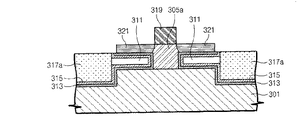
【解決手段】基板301上に形成された一対のボイド領域311と一対の不純物パターン321を有するエピタキシャルパターンと、一対の不純物パターン上のゲート電極319とを含み、前記一対のボイド領域の各々は基板と前記一対の不純物領域との間に位置し、前記一対の不純物領域の各々は少なくとも一対のボイド領域と一部重畳する。
【選択図】図1B
Description
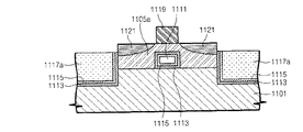
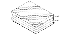
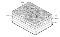
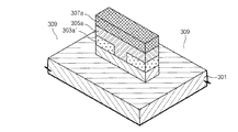
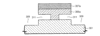
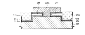
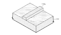
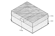
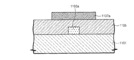
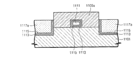
303,1103 エピタキシャル犠牲膜
303a,1103a エピタキシャル犠牲膜パターン
305,1105 エピタキシャル膜
305a,1105a エピタキシャル膜パターン
307a,1107a マスクパターン
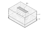
300,1109 トレンチ
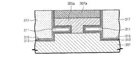
311,1111 空の空間領域
313,1113 熱酸化膜
315,1115 ライナ窒化膜
317,1117 素子分離領域
319,1119 ゲート電極
321,1121 不純物拡散領域
Claims (32)
- 基板と、
前記基板上に配置され、一対の不純物拡散領域及び一対のボイド領域を有するエピタキシャルパターンと、
前記一対の不純物拡散領域の間のエピタキシャルパターン上に位置するゲート電極と、を含み、
前記一対のボイド領域の各々は基板と前記一対の不純物拡散領域との間に位置し、
前記一対の不純物拡散領域の各々は少なくとも一対のボイド領域の各々と一部重畳することを特徴とする半導体素子。 - 前記エピタキシャルパターンは前記半導体パターンと直接接触することを特徴とする請求項1に記載の半導体素子。
- 前記エピタキシャルパターンはシリコンまたはシリコン−ゲルマニウムを含むことを特徴とする請求項1に記載の半導体素子。
- 前記ゲート電極はポリシリコンまたは金属シリサイドを含むことを特徴とする請求項1に記載の半導体素子。
- 前記一対のボイド領域は絶縁物質で満たされることを特徴とする請求項1に記載の半導体素子。
- 前記エピタキシャルパターンに隣接した素子分離膜をさらに含み、前記素子分離膜は前記エピタキシャルパターンの上部の表面よりも低い上部の表面を有することを特徴とする請求項1に記載の半導体素子。
- 基板と、
前記基板上に配置され、一対の不純物拡散領域及び前記一対の不純物拡散領域の間に形成されたボイド領域を有するエピタキシャルパターンと、
前記一対の不純物拡散領域の間のエピタキシャルパターン上に位置するゲート電極と、を含み、
前記ゲート電極は少なくとも前記ボイド領域と一部重畳することを特徴とする半導体素子。 - 前記エピタキシャルパターンは直接前記基板と接触することを特徴とする請求項7に記載の半導体素子。
- 前記エピタキシャルパターンはシリコンまたはシリコン−ゲルマニウムを含むことを特徴とする請求項7に記載の半導体素子。
- 前記ゲート電極はポリシリコンまたは金属シリサイドを含むことを特徴とする請求項7に記載の半導体素子。
- 前記ボイド領域は絶縁物質で満たされることを特徴とする請求項7に記載の半導体素子。
- 前記エピタキシャルパターンに隣接した素子分離膜をさらに含み、前記素子分離膜は前記エピタキシャルパターンの上部の表面よりも低い上部の表面を有することを特徴とする請求項7に記載の半導体素子。
- 素子分離領域を具備する半導体基板と、
前記素子分離領域により限定され、前記基板上に配置され、前記素子分離領域とともに空の空間領域を形成するエピタキシャルパターンと、
前記エピタキシャル膜パターン及び前記素子分離領域を横切るゲート電極と、
前記ゲート電極の両側のエピタキシャル膜パターンに形成された不純物拡散領域と、
を含むことを特徴とする半導体素子。 - 前記空の空間領域は前記ゲート電極の下部のエピタキシャル膜パターンと前記基板との間に位置することを特徴とする請求項13に記載の半導体素子。
- 前記空の空間領域は前記ゲート電極の両側のエピタキシャル膜パターンと前記基板との間に位置することを特徴とする請求項13に記載の半導体素子。
- 前記素子分離領域は前記空の空間領域に拡張され、それを満たすことを特徴とする請求項13に記載の半導体素子。
- 前記素子分離領域の上部の表面は前記エピタキシャル膜パターンの上部よりもさらに低いことを特徴とする請求項13に記載の半導体素子。
- 前記エピタキシャル膜パターンはシリコンまたはシリコン−ゲルマニウムからなることを特徴とする請求項13に記載の半導体素子。
- 半導体基板上にエピタキシャル犠牲膜パターンを形成する段階と、
前記エピタキシャル犠牲膜パターン及びそれにより露出した基板上にエピタキシャル膜を形成する段階と、
前記エピタキシャル膜、エピタキシャル犠牲膜パターン及び基板の一部の厚さをエッチングして、エピタキシャル膜パターン及び素子分離トレンチを形成する段階と、
前記トレンチにより露出したエッチングされたエピタキシャル犠牲膜パターンを除去する段階と、
前記トレンチを満たし、前記エピタキシャル膜パターンの上部の表面よりもさらに低い素子分離領域を形成する段階と、
前記エピタキシャル膜パターンを横切るゲート電極を形成する段階と、
前記ゲート電極の両側のエピタキシャル膜パターンに不純物拡散領域を形成する段階と、
を含むことを特徴とする半導体素子製造方法。 - 前記エピタキシャル膜パターン及び素子分離トレンチを形成する段階は、
前記エピタキシャル膜上にマスクパターンを形成する段階と、
前記マスクパターンをエッチングマスクとして使用して、前記エピタキシャル膜、エピタキシャル犠牲膜パターン及び基板の一部の厚さをエッチングする段階と、を含み、
前記素子分離領域を形成する段階は、
前記エッチングトレンチを満たすように、前記マスクパターン上に絶縁物質を形成する段階と、
前記マスクパターンが露出するまで前記絶縁物質を平坦化エッチングする段階と、
前記露出したマスクパターンを除去する段階と、
前記エピタキシャル膜パターンよりも低くなるように前記絶縁物質をエッチングする段階と、を含む
ことを特徴とする請求項19に記載の半導体素子製造方法。 - 前記絶縁物質を形成する段階の前に、
熱酸化工程を進行して、前記エッチングされたエピタキシャル犠牲膜パターン及び前記トレンチ上に熱酸化膜を形成する段階と、
前記熱酸化膜上にライナ窒化膜を形成する段階と、
をさらに含むことを特徴とする請求項20に記載の半導体素子製造方法。 - 前記絶縁物質は前記エッチングされたエピタキシャル犠牲膜パターンが除去された領域も満たすことを特徴とする請求項19に記載の半導体素子製造方法。
- 前記エッチングされたエピタキシャル犠牲膜パターンが除去された領域は前記ゲート電極の両側の前記エピタキシャル膜パターンと前記基板との間に位置することを特徴とする請求項19に記載の半導体素子製造方法。
- 前記エッチングされたエピタキシャル犠牲膜パターンが除去された領域は前記ゲート電極の下部の前記エピタキシャル膜パターンと前記基板との間に位置することを特徴とする請求項19に記載の半導体素子製造方法。
- 前記エピタキシャル膜はシリコン膜で形成されることを特徴とする請求項19に記載の半導体素子製造方法。
- 前記エピタキシャル犠牲膜はシリコンと結晶構造が同一であり、格子常数が類似な物質で形成されることを特徴とする請求項25に記載の半導体素子製造方法。
- 前記エピタキシャル犠牲膜はシリコン−ゲルマニウム、酸化セリウム、フッ化カルシウムのうちのいずれか一つ、またはこれらの組み合わせ膜で形成されることを特徴とする請求項26に記載の半導体素子製造方法。
- 前記エピタキシャル犠牲膜はシリコン−ゲルマニウム、酸化セリウム、フッ化カルシウムのうちのいずれか一つ、またはこれらの組み合わせ膜で形成されることを特徴とする請求項19に記載の半導体素子製造方法。
- 前記エピタキシャル犠牲膜はシリコンからなり、前記エピタキシャル膜はシリコン−ゲルマニウムからなることを特徴とする請求項19に記載の半導体素子製造方法。
- 半導体基板に電気的に接続され、前記半導体基板との間に絶縁領域を形成するように、前記半導体基板上に配置されたエピタキシャルシリコン膜と、
前記エピタキシャルシリコン膜を横切るゲート電極と、
前記ゲート電極の両側のエピタキシャルシリコン膜に形成された不純物拡散領域と、
を含むことを特徴とする半導体素子。 - 前記絶縁領域は前記不純物拡散領域と前記基板との間に位置することを特徴とする請求項30に記載の半導体素子。
- 前記絶縁領域は前記ゲート電極の下部のエピタキシャルシリコン膜と前記基板との間に位置することを特徴とする請求項30に記載の半導体素子。
Applications Claiming Priority (2)
| Application Number | Priority Date | Filing Date | Title |
|---|---|---|---|
| KR2003-028287 | 2003-05-02 | ||
| KR1020030028287A KR100553683B1 (ko) | 2003-05-02 | 2003-05-02 | 반도체 소자 및 그 제조 방법 |
Publications (2)
| Publication Number | Publication Date |
|---|---|
| JP2004336052A true JP2004336052A (ja) | 2004-11-25 |
| JP4981245B2 JP4981245B2 (ja) | 2012-07-18 |
Family
ID=33308396
Family Applications (1)
| Application Number | Title | Priority Date | Filing Date |
|---|---|---|---|
| JP2004136486A Expired - Fee Related JP4981245B2 (ja) | 2003-05-02 | 2004-04-30 | 半導体素子製造方法 |
Country Status (4)
| Country | Link |
|---|---|
| US (2) | US20040217434A1 (ja) |
| JP (1) | JP4981245B2 (ja) |
| KR (1) | KR100553683B1 (ja) |
| CN (1) | CN100479159C (ja) |
Cited By (13)
| Publication number | Priority date | Publication date | Assignee | Title |
|---|---|---|---|---|
| JP2006344943A (ja) * | 2005-06-09 | 2006-12-21 | Samsung Electronics Co Ltd | トレンチ分離領域を有するmos電界効果トランジスタ及びその製造方法 |
| JP2007005759A (ja) * | 2005-06-27 | 2007-01-11 | Hynix Semiconductor Inc | 半導体素子及びその製造方法 |
| JP2007027231A (ja) * | 2005-07-13 | 2007-02-01 | Seiko Epson Corp | 半導体装置の製造方法及び、半導体装置 |
| JP2007027232A (ja) * | 2005-07-13 | 2007-02-01 | Seiko Epson Corp | 半導体装置及びその製造方法 |
| JP2007300062A (ja) * | 2006-04-28 | 2007-11-15 | Hynix Semiconductor Inc | 半導体素子の製造方法 |
| JP2008010876A (ja) * | 2006-06-29 | 2008-01-17 | Internatl Business Mach Corp <Ibm> | フィンfetデバイスの構造およびその製造方法 |
| JP2008294408A (ja) * | 2007-04-27 | 2008-12-04 | Semiconductor Energy Lab Co Ltd | 半導体装置及びその作製方法 |
| JP2008294407A (ja) * | 2007-04-25 | 2008-12-04 | Semiconductor Energy Lab Co Ltd | 半導体装置及びその作製方法 |
| JP2010118539A (ja) * | 2008-11-13 | 2010-05-27 | Toshiba Corp | 不揮発性半導体記憶装置 |
| US7816725B2 (en) | 2005-12-06 | 2010-10-19 | Samsung Electronics Co., Ltd. | Semiconductor devices and methods of fabricating the same |
| JP2012227509A (ja) * | 2011-04-05 | 2012-11-15 | Fujitsu Semiconductor Ltd | 半導体装置およびその製造方法 |
| JP2014505995A (ja) * | 2010-12-01 | 2014-03-06 | インテル コーポレイション | シリコン及びシリコンゲルマニウムのナノワイヤ構造 |
| US8987794B2 (en) | 2011-12-23 | 2015-03-24 | Intel Coporation | Non-planar gate all-around device and method of fabrication thereof |
Families Citing this family (54)
| Publication number | Priority date | Publication date | Assignee | Title |
|---|---|---|---|---|
| CN100433257C (zh) * | 2004-01-15 | 2008-11-12 | 野田优 | 制造单晶薄膜的方法 |
| KR100598098B1 (ko) * | 2004-02-06 | 2006-07-07 | 삼성전자주식회사 | 매몰 절연 영역을 갖는 모오스 전계 효과 트랜지스터 및그 제조 방법 |
| FR2899017A1 (fr) * | 2006-03-21 | 2007-09-28 | St Microelectronics Sa | Procede de realisation d'un transistor a canal comprenant du germanium |
| JP4360413B2 (ja) * | 2007-03-28 | 2009-11-11 | セイコーエプソン株式会社 | 半導体装置の製造方法 |
| JP2009182114A (ja) * | 2008-01-30 | 2009-08-13 | Elpida Memory Inc | 半導体装置およびその製造方法 |
| KR101168468B1 (ko) | 2008-07-14 | 2012-07-26 | 에스케이하이닉스 주식회사 | 반도체 소자의 제조 방법 |
| CN102104069B (zh) | 2009-12-16 | 2012-11-21 | 中国科学院微电子研究所 | 鳍式晶体管结构及其制作方法 |
| CN102117829B (zh) | 2009-12-30 | 2012-11-21 | 中国科学院微电子研究所 | 鳍式晶体管结构及其制作方法 |
| CN102157554A (zh) * | 2010-02-12 | 2011-08-17 | 中国科学院微电子研究所 | 鳍式晶体管结构及其制作方法 |
| KR101674179B1 (ko) * | 2010-04-06 | 2016-11-10 | 삼성전자주식회사 | 전계 효과 트랜지스터를 포함하는 반도체 소자 및 그 형성 방법 |
| CN102222691A (zh) * | 2010-04-13 | 2011-10-19 | 联合大学 | 高驱动电流三维多重闸极晶体管及其制法 |
| US8610211B2 (en) * | 2010-07-23 | 2013-12-17 | International Business Machines Corporation | Semiconductor-on-insulator (SOI) structure with selectively placed sub-insulator layer void(s) and method of forming the SOI structure |
| US8492235B2 (en) * | 2010-12-29 | 2013-07-23 | Globalfoundries Singapore Pte. Ltd. | FinFET with stressors |
| FR2970812B1 (fr) * | 2011-01-24 | 2013-11-15 | Commissariat Energie Atomique | Dispositif a effet de champ avec une faible capacité de jonction |
| US8426289B2 (en) * | 2011-04-14 | 2013-04-23 | Robert Bosch Gmbh | Wafer with spacer including horizontal member |
| CN103515283B (zh) * | 2012-06-25 | 2016-03-30 | 中国科学院微电子研究所 | 半导体器件制造方法 |
| CN103811340B (zh) | 2012-11-09 | 2017-07-14 | 中国科学院微电子研究所 | 半导体器件及其制造方法 |
| CN103811345B (zh) * | 2012-11-09 | 2016-08-03 | 中国科学院微电子研究所 | 半导体器件及其制造方法 |
| US8759874B1 (en) * | 2012-11-30 | 2014-06-24 | Stmicroelectronics, Inc. | FinFET device with isolated channel |
| US8956942B2 (en) | 2012-12-21 | 2015-02-17 | Stmicroelectronics, Inc. | Method of forming a fully substrate-isolated FinFET transistor |
| CN103928333B (zh) * | 2013-01-15 | 2019-03-12 | 中国科学院微电子研究所 | 半导体器件及其制造方法 |
| KR102017625B1 (ko) | 2013-05-10 | 2019-10-22 | 삼성전자주식회사 | 반도체 장치 및 그 제조방법 |
| US9123585B1 (en) | 2014-02-11 | 2015-09-01 | International Business Machines Corporation | Method to form group III-V and Si/Ge FINFET on insulator |
| US9129863B2 (en) | 2014-02-11 | 2015-09-08 | International Business Machines Corporation | Method to form dual channel group III-V and Si/Ge FINFET CMOS |
| CN105261587A (zh) * | 2014-07-16 | 2016-01-20 | 中国科学院微电子研究所 | 半导体器件及其制造方法 |
| CN105322012B (zh) * | 2014-07-16 | 2018-12-04 | 中国科学院微电子研究所 | 半导体器件及其制造方法 |
| CN105322010B (zh) * | 2014-07-16 | 2019-05-28 | 中国科学院微电子研究所 | 半导体器件的制造方法 |
| CN105304629B (zh) * | 2014-07-16 | 2018-07-13 | 中国科学院微电子研究所 | 半导体器件及其制造方法 |
| US9536999B2 (en) | 2014-09-08 | 2017-01-03 | Infineon Technologies Ag | Semiconductor device with control structure including buried portions and method of manufacturing |
| US9935126B2 (en) | 2014-09-08 | 2018-04-03 | Infineon Technologies Ag | Method of forming a semiconductor substrate with buried cavities and dielectric support structures |
| JP6620318B2 (ja) | 2014-11-27 | 2019-12-18 | パナソニックIpマネジメント株式会社 | シート状伸縮性構造体 |
| KR102327974B1 (ko) * | 2014-12-22 | 2021-11-17 | 인텔 코포레이션 | 에어갭 통합 커패시턴스 이익을 갖는 비아 자체 정렬 및 단락 개선 |
| KR102315275B1 (ko) * | 2015-10-15 | 2021-10-20 | 삼성전자 주식회사 | 집적회로 소자 및 그 제조 방법 |
| CN105552126A (zh) * | 2015-12-15 | 2016-05-04 | 上海集成电路研发中心有限公司 | 鳍式场效应晶体管及其制备方法 |
| CN106328715B (zh) * | 2016-08-17 | 2019-02-01 | 深圳市华星光电技术有限公司 | 薄膜晶体管及其制作方法 |
| DE102016119799B4 (de) * | 2016-10-18 | 2020-08-06 | Infineon Technologies Ag | Integrierte schaltung, die einen vergrabenen hohlraum enthält, und herstellungsverfahren |
| US10461152B2 (en) | 2017-07-10 | 2019-10-29 | Globalfoundries Inc. | Radio frequency switches with air gap structures |
| US10833153B2 (en) | 2017-09-13 | 2020-11-10 | Globalfoundries Inc. | Switch with local silicon on insulator (SOI) and deep trench isolation |
| US10446643B2 (en) * | 2018-01-22 | 2019-10-15 | Globalfoundries Inc. | Sealed cavity structures with a planar surface |
| US10720494B2 (en) * | 2018-01-22 | 2020-07-21 | Globalfoundries Inc. | Field-effect transistors with airgaps |
| US11410872B2 (en) | 2018-11-30 | 2022-08-09 | Globalfoundries U.S. Inc. | Oxidized cavity structures within and under semiconductor devices |
| US10923577B2 (en) | 2019-01-07 | 2021-02-16 | Globalfoundries U.S. Inc. | Cavity structures under shallow trench isolation regions |
| KR102411803B1 (ko) * | 2019-04-23 | 2022-06-22 | 타이완 세미콘덕터 매뉴팩쳐링 컴퍼니 리미티드 | 반도체 디바이스 및 그 제조 방법 |
| US11233140B2 (en) | 2019-04-23 | 2022-01-25 | Taiwan Semiconductor Manufacturing Company, Ltd. | Semiconductor device and manufacturing method thereof |
| US11916107B2 (en) * | 2019-04-23 | 2024-02-27 | Taiwan Semiconductor Manufacturing Company, Ltd. | Semiconductor device and manufacturing method thereof |
| US11393713B2 (en) * | 2019-04-23 | 2022-07-19 | Taiwan Semiconductor Manufacturing Co., Ltd. | Semiconductor device and manufacturing method therefore |
| US11557650B2 (en) | 2019-04-23 | 2023-01-17 | Taiwan Semiconductor Manufacturing Co., Ltd. | Semiconductor device and manufacturing method thereof |
| KR102355231B1 (ko) * | 2019-04-23 | 2022-01-25 | 타이완 세미콘덕터 매뉴팩쳐링 컴퍼니 리미티드 | 반도체 디바이스 및 그 제조 방법 |
| DE102020103046B4 (de) * | 2019-04-23 | 2024-03-28 | Taiwan Semiconductor Manufacturing Co., Ltd. | Halbleitervorrichtung und herstellungsverfahren dafür |
| TWI805919B (zh) * | 2019-04-23 | 2023-06-21 | 台灣積體電路製造股份有限公司 | 半導體裝置及其製造方法 |
| US11127816B2 (en) | 2020-02-14 | 2021-09-21 | Globalfoundries U.S. Inc. | Heterojunction bipolar transistors with one or more sealed airgap |
| US11817479B2 (en) * | 2021-09-29 | 2023-11-14 | Globalfoundries U.S. Inc. | Transistor with air gap under raised source/drain region in bulk semiconductor substrate |
| US11677000B2 (en) | 2021-10-07 | 2023-06-13 | Globalfoundries U.S. Inc. | IC structure including porous semiconductor layer under trench isolations adjacent source/drain regions |
| JP7715996B2 (ja) * | 2021-12-14 | 2025-07-31 | ユナイテッド・セミコンダクター・ジャパン株式会社 | 半導体装置及び半導体装置の製造方法 |
Citations (6)
| Publication number | Priority date | Publication date | Assignee | Title |
|---|---|---|---|---|
| JPH01214064A (ja) * | 1988-02-22 | 1989-08-28 | Nec Corp | 絶縁ゲート電界効果トランジスタおよびその製造方法 |
| JPH05299647A (ja) * | 1992-04-24 | 1993-11-12 | Sanyo Electric Co Ltd | Mos電界効果トランジスタとその製造方法 |
| JPH06334178A (ja) * | 1993-05-27 | 1994-12-02 | Toshiba Corp | 半導体装置及びその製造方法 |
| JPH0851198A (ja) * | 1994-08-08 | 1996-02-20 | Matsushita Electron Corp | 半導体装置 |
| JP2000012858A (ja) * | 1998-04-24 | 2000-01-14 | Toshiba Corp | 半導体装置およびその製造方法 |
| JP2000294781A (ja) * | 1999-03-19 | 2000-10-20 | France Telecom | 漏れ電流の低い半導体素子及びその製造方法 |
Family Cites Families (10)
| Publication number | Priority date | Publication date | Assignee | Title |
|---|---|---|---|---|
| JP2886420B2 (ja) * | 1992-10-23 | 1999-04-26 | 三菱電機株式会社 | 半導体装置の製造方法 |
| US5891763A (en) * | 1997-10-22 | 1999-04-06 | Wanlass; Frank M. | Damascene pattering of SOI MOS transistors |
| JPH11145147A (ja) * | 1997-11-11 | 1999-05-28 | Nec Corp | 半導体装置および半導体装置の製造方法 |
| US5972758A (en) * | 1997-12-04 | 1999-10-26 | Intel Corporation | Pedestal isolated junction structure and method of manufacture |
| US6235560B1 (en) * | 1999-08-16 | 2001-05-22 | Agere Systems Guardian Corp. | Silicon-germanium transistor and associated methods |
| KR100304713B1 (ko) * | 1999-10-12 | 2001-11-02 | 윤종용 | 부분적인 soi 구조를 갖는 반도체소자 및 그 제조방법 |
| US6333235B1 (en) * | 2000-04-12 | 2001-12-25 | Industrial Technologyresearch Institute | Method for forming SiGe bipolar transistor |
| KR100340878B1 (ko) * | 2000-06-28 | 2002-06-20 | 박종섭 | 에스오아이 소자의 제조방법 |
| US6583025B2 (en) * | 2000-07-10 | 2003-06-24 | Samsung Electronics Co., Ltd. | Method of forming a trench isolation structure comprising annealing the oxidation barrier layer thereof in a furnace |
| US7122431B2 (en) * | 2003-01-16 | 2006-10-17 | Samsung Electronics Co., Ltd. | Methods of fabrication metal oxide semiconductor (MOS) transistors having buffer regions below source and drain regions |
-
2003
- 2003-05-02 KR KR1020030028287A patent/KR100553683B1/ko not_active Expired - Fee Related
-
2004
- 2004-04-30 JP JP2004136486A patent/JP4981245B2/ja not_active Expired - Fee Related
- 2004-04-30 US US10/835,760 patent/US20040217434A1/en not_active Abandoned
- 2004-05-08 CN CNB2004100385852A patent/CN100479159C/zh not_active Expired - Fee Related
-
2008
- 2008-04-22 US US12/107,468 patent/US20080194065A1/en not_active Abandoned
Patent Citations (6)
| Publication number | Priority date | Publication date | Assignee | Title |
|---|---|---|---|---|
| JPH01214064A (ja) * | 1988-02-22 | 1989-08-28 | Nec Corp | 絶縁ゲート電界効果トランジスタおよびその製造方法 |
| JPH05299647A (ja) * | 1992-04-24 | 1993-11-12 | Sanyo Electric Co Ltd | Mos電界効果トランジスタとその製造方法 |
| JPH06334178A (ja) * | 1993-05-27 | 1994-12-02 | Toshiba Corp | 半導体装置及びその製造方法 |
| JPH0851198A (ja) * | 1994-08-08 | 1996-02-20 | Matsushita Electron Corp | 半導体装置 |
| JP2000012858A (ja) * | 1998-04-24 | 2000-01-14 | Toshiba Corp | 半導体装置およびその製造方法 |
| JP2000294781A (ja) * | 1999-03-19 | 2000-10-20 | France Telecom | 漏れ電流の低い半導体素子及びその製造方法 |
Cited By (26)
| Publication number | Priority date | Publication date | Assignee | Title |
|---|---|---|---|---|
| JP2006344943A (ja) * | 2005-06-09 | 2006-12-21 | Samsung Electronics Co Ltd | トレンチ分離領域を有するmos電界効果トランジスタ及びその製造方法 |
| US8416599B2 (en) | 2005-06-09 | 2013-04-09 | Samsung Electronics Co., Ltd. | Metal oxide semiconductor (MOS) field effect transistor having trench isolation region and method of fabricating the same |
| JP2007005759A (ja) * | 2005-06-27 | 2007-01-11 | Hynix Semiconductor Inc | 半導体素子及びその製造方法 |
| JP2007027231A (ja) * | 2005-07-13 | 2007-02-01 | Seiko Epson Corp | 半導体装置の製造方法及び、半導体装置 |
| JP2007027232A (ja) * | 2005-07-13 | 2007-02-01 | Seiko Epson Corp | 半導体装置及びその製造方法 |
| US8298899B2 (en) | 2005-12-06 | 2012-10-30 | Samsung Electronics Co., Ltd. | Semiconductor devices and methods of fabricating the same |
| US7816725B2 (en) | 2005-12-06 | 2010-10-19 | Samsung Electronics Co., Ltd. | Semiconductor devices and methods of fabricating the same |
| JP2007300062A (ja) * | 2006-04-28 | 2007-11-15 | Hynix Semiconductor Inc | 半導体素子の製造方法 |
| JP2008010876A (ja) * | 2006-06-29 | 2008-01-17 | Internatl Business Mach Corp <Ibm> | フィンfetデバイスの構造およびその製造方法 |
| JP2008294407A (ja) * | 2007-04-25 | 2008-12-04 | Semiconductor Energy Lab Co Ltd | 半導体装置及びその作製方法 |
| JP2008294408A (ja) * | 2007-04-27 | 2008-12-04 | Semiconductor Energy Lab Co Ltd | 半導体装置及びその作製方法 |
| US8664078B2 (en) | 2007-04-27 | 2014-03-04 | Semiconductor Energy Laboratory Co., Ltd. | Manufacturing method of semiconductor device on cavities |
| US8928062B2 (en) | 2008-11-13 | 2015-01-06 | Kabushiki Kaisha Toshiba | Nonvolatile semiconductor memory device and manufacturing method thereof |
| JP2010118539A (ja) * | 2008-11-13 | 2010-05-27 | Toshiba Corp | 不揮発性半導体記憶装置 |
| US9129829B2 (en) | 2010-12-01 | 2015-09-08 | Intel Corporation | Silicon and silicon germanium nanowire structures |
| JP2014505995A (ja) * | 2010-12-01 | 2014-03-06 | インテル コーポレイション | シリコン及びシリコンゲルマニウムのナノワイヤ構造 |
| US9595581B2 (en) | 2010-12-01 | 2017-03-14 | Intel Corporation | Silicon and silicon germanium nanowire structures |
| KR20190022931A (ko) * | 2010-12-01 | 2019-03-06 | 인텔 코포레이션 | 실리콘 및 실리콘 게르마늄 나노와이어 구조물 |
| KR102013115B1 (ko) | 2010-12-01 | 2019-08-21 | 인텔 코포레이션 | 실리콘 및 실리콘 게르마늄 나노와이어 구조물 |
| US10636871B2 (en) | 2010-12-01 | 2020-04-28 | Intel Corporation | Silicon and silicon germanium nanowire structures |
| US10991799B2 (en) | 2010-12-01 | 2021-04-27 | Sony Corporation | Silicon and silicon germanium nanowire structures |
| US12142634B2 (en) | 2010-12-01 | 2024-11-12 | Sony Group Corporation | Silicon and silicon germanium nanowire structures |
| JP2012227509A (ja) * | 2011-04-05 | 2012-11-15 | Fujitsu Semiconductor Ltd | 半導体装置およびその製造方法 |
| US8987794B2 (en) | 2011-12-23 | 2015-03-24 | Intel Coporation | Non-planar gate all-around device and method of fabrication thereof |
| US10418487B2 (en) | 2011-12-23 | 2019-09-17 | Intel Corporation | Non-planar gate all-around device and method of fabrication thereof |
| USRE50222E1 (en) | 2011-12-23 | 2024-11-26 | Sony Group Corporation | Non-planar gate all-around device and method of fabrication thereof |
Also Published As
| Publication number | Publication date |
|---|---|
| US20080194065A1 (en) | 2008-08-14 |
| KR20040094498A (ko) | 2004-11-10 |
| KR100553683B1 (ko) | 2006-02-24 |
| CN100479159C (zh) | 2009-04-15 |
| US20040217434A1 (en) | 2004-11-04 |
| JP4981245B2 (ja) | 2012-07-18 |
| CN1542965A (zh) | 2004-11-03 |
Similar Documents
| Publication | Publication Date | Title |
|---|---|---|
| JP4981245B2 (ja) | 半導体素子製造方法 | |
| CN106340455B (zh) | 半导体元件及其制作方法 | |
| US11251184B2 (en) | Semiconductor arrangement having continuous spacers and method of manufacturing the same | |
| KR101835655B1 (ko) | 핀 전계 효과 트랜지스터 및 이의 제조 방법 | |
| US7265418B2 (en) | Semiconductor devices having field effect transistors | |
| JP5319046B2 (ja) | ベリード酸化膜を具備する半導体装置の製造方法及びこれを具備する半導体装置 | |
| US7972914B2 (en) | Semiconductor device with FinFET and method of fabricating the same | |
| JP5075320B2 (ja) | 三次元構造のチャンネルを備えるモストランジスタの製造方法 | |
| TWI404145B (zh) | 拉緊的絕緣層上覆矽層結構及其製備方法 | |
| US20070048947A1 (en) | Multi-structured Si-fin and method of manufacture | |
| JP2009267021A (ja) | 半導体装置及びその製造方法 | |
| WO2009141977A1 (ja) | 半導体装置およびその製造方法 | |
| US7166514B2 (en) | Semiconductor device and method of manufacturing the same | |
| CN100550418C (zh) | 在源和漏区下面具有缓冲区的金属氧化物半导体(mos)晶体管及其制造方法 | |
| JP2006049627A (ja) | 半導体装置及びその製造方法 | |
| US6998682B2 (en) | Method of forming a partially depleted silicon on insulator (PDSOI) transistor with a pad lock body extension | |
| JP2008028357A (ja) | 半導体素子及びその製造方法 | |
| JP4519442B2 (ja) | Mosトランジスター及びその製造方法 | |
| JP5547986B2 (ja) | 半導体装置およびその製造方法 | |
| KR100495668B1 (ko) | 반도체 소자 및 그 제조 방법 | |
| US20090321821A1 (en) | Semiconductor device having recess gate and method of fabricating the same | |
| JP4434832B2 (ja) | 半導体装置、及びその製造方法 | |
| WO2009147772A1 (ja) | 半導体装置及びその製造方法 | |
| KR20070095062A (ko) | 핀 전계 효과 트랜지스터 및 그 제조방법 | |
| KR100506455B1 (ko) | 반도체소자의 형성방법 |
Legal Events
| Date | Code | Title | Description |
|---|---|---|---|
| A621 | Written request for application examination |
Free format text: JAPANESE INTERMEDIATE CODE: A621 Effective date: 20061109 |
|
| A977 | Report on retrieval |
Free format text: JAPANESE INTERMEDIATE CODE: A971007 Effective date: 20100628 |
|
| A131 | Notification of reasons for refusal |
Free format text: JAPANESE INTERMEDIATE CODE: A131 Effective date: 20100831 |
|
| A521 | Request for written amendment filed |
Free format text: JAPANESE INTERMEDIATE CODE: A523 Effective date: 20101111 |
|
| A131 | Notification of reasons for refusal |
Free format text: JAPANESE INTERMEDIATE CODE: A131 Effective date: 20110329 |
|
| A521 | Request for written amendment filed |
Free format text: JAPANESE INTERMEDIATE CODE: A523 Effective date: 20110613 |
|
| A131 | Notification of reasons for refusal |
Free format text: JAPANESE INTERMEDIATE CODE: A131 Effective date: 20111018 |
|
| TRDD | Decision of grant or rejection written | ||
| A01 | Written decision to grant a patent or to grant a registration (utility model) |
Free format text: JAPANESE INTERMEDIATE CODE: A01 Effective date: 20120321 |
|
| A01 | Written decision to grant a patent or to grant a registration (utility model) |
Free format text: JAPANESE INTERMEDIATE CODE: A01 |
|
| A61 | First payment of annual fees (during grant procedure) |
Free format text: JAPANESE INTERMEDIATE CODE: A61 Effective date: 20120420 |
|
| FPAY | Renewal fee payment (event date is renewal date of database) |
Free format text: PAYMENT UNTIL: 20150427 Year of fee payment: 3 |
|
| R150 | Certificate of patent or registration of utility model |
Free format text: JAPANESE INTERMEDIATE CODE: R150 |
|
| LAPS | Cancellation because of no payment of annual fees |