JP2005225735A - Production method for dielectric porcelain composition - Google Patents
Production method for dielectric porcelain composition Download PDFInfo
- Publication number
- JP2005225735A JP2005225735A JP2004037581A JP2004037581A JP2005225735A JP 2005225735 A JP2005225735 A JP 2005225735A JP 2004037581 A JP2004037581 A JP 2004037581A JP 2004037581 A JP2004037581 A JP 2004037581A JP 2005225735 A JP2005225735 A JP 2005225735A
- Authority
- JP
- Japan
- Prior art keywords
- powder
- site
- dielectric
- raw material
- ceramic composition
- Prior art date
- Legal status (The legal status is an assumption and is not a legal conclusion. Google has not performed a legal analysis and makes no representation as to the accuracy of the status listed.)
- Withdrawn
Links
Images
Landscapes
- Compositions Of Oxide Ceramics (AREA)
- Inorganic Insulating Materials (AREA)
Abstract
Description
本発明は、誘電体磁器組成物の製造方法に関するものである。 The present invention relates to a method for producing a dielectric ceramic composition.
近年、通信機の小型化、軽量化、高速化が強く望まれている。その中で、デジタル携帯電話等の携帯移動体通信、衛星通信に使用される電波の周波数帯域はメガからギガHz帯(「GHz帯」という)の高周波帯域のものが使用されている。使用される通信機器の急速な発展の中で、匡体及び基板、電子素子の小型高密度実装化が図られているが、高周波帯域に対応した通信機器の小型化、軽量化をより一層推進するためには、通信機器に使用される基板等の材料はGHz帯において高周波伝送特性が優れた(誘電損失が小さい)ものでなければならない。ここで、誘電損失は周波数と基板の比誘電率εrと誘電正接(以下tanδと記載する)の積に比例する。よって、誘電損失を小さくするためには基板のtanδを小さくしなければならない。また、基板中では電磁波の波長が1/(εr)0.5に短縮されるため、比誘電率εrが大きい程基板の小型化が可能である。以上のことから高周波帯域で使用される小型の通信機器、電子機器、情報機器に用いる回路基板としては、比誘電率εrが高く、かつQf(品質係数Q=1/tanδ、f=共振周波数)が大きいことが要求されている。 In recent years, miniaturization, weight reduction, and speeding up of communication devices have been strongly desired. Among them, the frequency band of radio waves used for portable mobile communications such as digital cellular phones and satellite communications is in the high frequency band of mega to giga Hz band (referred to as “GHz band”). Amid the rapid development of used communication equipment, the housing, board, and electronic elements have been miniaturized and densely mounted. However, the communication equipment that supports the high frequency band has been further reduced in size and weight. In order to achieve this, materials such as substrates used in communication equipment must be excellent in high-frequency transmission characteristics (low dielectric loss) in the GHz band. Here, the dielectric loss is proportional to the product of the frequency, the relative dielectric constant εr of the substrate, and the dielectric loss tangent (hereinafter referred to as tan δ). Therefore, in order to reduce the dielectric loss, tan δ of the substrate must be reduced. Further, since the wavelength of the electromagnetic wave in the substrate is shortened to 1 / (εr) 0.5 , the substrate can be downsized as the relative dielectric constant εr increases. As described above, a circuit board used for a small communication device, electronic device, or information device used in a high frequency band has a high relative dielectric constant εr and Qf (quality factor Q = 1 / tan δ, f = resonance frequency). Is required to be large.
このような回路基板の材料としては、無機材料としての誘電体材料(焼成物)、有機材料としてのフッ素樹脂等が用いられている。ところが、誘電体材料からなる基板は、寸法精度、加工性に難点があり、脆いため欠けや割れが生じやすいという問題点があった。他方、樹脂等の有機材料からなる基板は、成形性及び加工性に優れるという利点はあるが、比誘電率εrが小さいという問題があった。このため、近年、両者の利点を有する基板として、例えば特許文献1(特開2003−128930号公報)、特許文献2(特開2003−151352号)において誘電体粉末と樹脂材料とからなる複合基板が開示されている。 As a material for such a circuit board, a dielectric material (baked product) as an inorganic material, a fluororesin as an organic material, or the like is used. However, a substrate made of a dielectric material has problems in dimensional accuracy and workability, and is fragile, so that there is a problem that chips and cracks are likely to occur. On the other hand, a substrate made of an organic material such as a resin has the advantage of being excellent in moldability and workability, but has a problem that the relative dielectric constant εr is small. Therefore, in recent years, as a substrate having both advantages, for example, a composite substrate made of a dielectric powder and a resin material in Patent Document 1 (Japanese Patent Laid-Open No. 2003-128930) and Patent Document 2 (Japanese Patent Laid-Open No. 2003-151352). Is disclosed.
誘電体材料としては、チタン酸バリウム、チタン酸ジルコン酸鉛等のABO3型の原子配列を持つペロブスカイト酸化物が通常用いられており、その粉末(誘電体粉末)の製造方法としては、液相法、気相法、フラックス法及び固相法が知られている。
液相法は、金属塩の水溶液あるいは有機溶媒溶液を出発原料として、水和物等の金属酸化物前駆体粉末を製造し、次いでこの前駆体粉末を焼成して2種類以上の金属元素を含む金属酸化物粉末を製造する方法である。液相法としては、沈殿法、共沈法、加水分解法等が知られている。
気相法は、金属蒸気あるいは金属化合物の気相状態での化学反応により金属酸化物粉末を製造する方法であり、粒度分布が狭く、凝集が少ない粉末が得られる利点がある。
フラックス法は、金属酸化物の混合粉末にフラックス成分を添加して焼成することにより金属酸化物粉末を製造する方法である。
As the dielectric material, a perovskite oxide having an ABO 3 type atomic arrangement such as barium titanate and lead zirconate titanate is usually used, and a method for producing the powder (dielectric powder) is a liquid phase. Methods, gas phase methods, flux methods and solid phase methods are known.
In the liquid phase method, a metal oxide precursor powder such as a hydrate is produced using a metal salt aqueous solution or an organic solvent solution as a starting material, and then the precursor powder is fired to contain two or more kinds of metal elements. This is a method for producing a metal oxide powder. As the liquid phase method, a precipitation method, a coprecipitation method, a hydrolysis method and the like are known.
The gas phase method is a method for producing a metal oxide powder by a chemical reaction of a metal vapor or a metal compound in a gas phase state, and has an advantage that a powder having a narrow particle size distribution and less aggregation is obtained.
The flux method is a method for producing a metal oxide powder by adding a flux component to a metal oxide mixed powder and firing it.
以上の液相法、気相法及びフラックス法により得られる誘電体粉末は、その粒径を微細とすることができるとともに粒度分布を狭くできるという利点がある。ここで、上述した複合基板を作製する場合、樹脂材料と混合される誘電体粉末は、複合基板が積層された際の層間を薄くする場合、その粒径が小さいことが望まれる。液相法、気相法及びフラックス法により得られる誘電体粉末は、その粒径が微細であるため、複合基板を作製する上で望ましい誘電体粉末の製造方法である。しかし、これらの方法により得られる誘電体粉末のコストが高いという問題がある。 The dielectric powder obtained by the above liquid phase method, gas phase method and flux method has the advantage that the particle size can be made fine and the particle size distribution can be narrowed. Here, when the composite substrate described above is manufactured, it is desirable that the dielectric powder mixed with the resin material has a small particle diameter when the interlayer when the composite substrate is laminated is thinned. Since the dielectric powder obtained by the liquid phase method, the gas phase method and the flux method has a fine particle size, it is a desirable method for producing a dielectric powder in producing a composite substrate. However, there is a problem that the cost of the dielectric powder obtained by these methods is high.
以上の方法に比べて低コストで誘電体粉末を得る方法として固相法が知られている。固相法は、金属酸化物、炭酸塩等の粉末を仮焼し、この仮焼物を粉砕した後に焼成し、得られた焼成物を粉砕するという工程を備えている。例えば、チタン酸バリウムを得ようという場合、TiO2粉末とBaCO3粉末を原料粉末として混合、仮焼、粉砕、焼成、焼成物の粉砕という工程を経て製造することができる。ところが、まず仮焼後の粉砕過程において、粉砕された粉末に歪が発生するため、その時点で誘電特性が劣化してしまう。ここで、焼成後の粉砕により粒径の小さな粉末を得るためには、仮焼後の粉砕においてもできる限り微細な粉砕を得る必要があるが、その場合粉砕時間を長くするあるいは粉砕条件を厳しくする必要があるため、得られた粉末の誘電特性は劣化してしまう。誘電特性を劣化させないために粉砕時間を短くすると、微細な誘電体粉末を得ることができない。したがって、これまでは、固相法による誘電体粉末を用いた複合基板は所望する特性を得がたいという問題があった。一方で、固相法によって、誘電特性の劣化が少ない粉末が得られれば、コスト的な点も含めて考えると、複合基板を得るために非常に望ましい誘電体粉末の製造方法になる。 A solid phase method is known as a method for obtaining dielectric powder at a lower cost than the above methods. The solid phase method includes a step of calcining a powder of metal oxide, carbonate, etc., crushing the calcined product, calcining it, and crushing the obtained calcined product. For example, when obtaining barium titanate, it can be manufactured through steps of mixing, calcining, pulverizing, baking, and pulverizing the baked product by mixing TiO 2 powder and BaCO 3 powder as raw material powders. However, first, distortion occurs in the pulverized powder in the pulverization process after calcination, and the dielectric characteristics deteriorate at that time. Here, in order to obtain a powder having a small particle size by pulverization after firing, it is necessary to obtain pulverization as fine as possible in pulverization after calcination. Therefore, the dielectric properties of the obtained powder are deteriorated. If the pulverization time is shortened in order not to deteriorate the dielectric characteristics, it is impossible to obtain a fine dielectric powder. Therefore, until now, there has been a problem that a composite substrate using a dielectric powder by a solid phase method cannot obtain desired characteristics. On the other hand, if a powder with little deterioration in dielectric properties can be obtained by the solid phase method, it becomes a very desirable method for producing a dielectric powder in order to obtain a composite substrate, considering the cost.
本発明は以上の背景に鑑み、固相法を用いながらも、誘電特性の劣化が抑制された微細な誘電体粉末を得ることのできる誘電体磁器組成物の製造方法を提供することを課題とする。 In view of the above background, the present invention has an object to provide a method for producing a dielectric ceramic composition capable of obtaining a fine dielectric powder in which deterioration of dielectric properties is suppressed while using a solid phase method. To do.
本発明が対象とするABO3型の原子配列を持つペロブスカイト酸化物を含む誘電体磁器組成物は、Aサイトを構成するためのAサイト原料粉末とBサイトを構成するためのBサイト原料粉末とを混合、焼成することにより得ることができる。例えば、(Sr,Ca)TiO3を得ようとする場合には、通常、Aサイト原料としてSrCO3粉末及びCaCO3粉末、Bサイト原料としてTiO2粉末を用意する。本発明者らの検討によれば、Bサイト原料の比表面積(BET法による値、本発明ではBET値という)を特定の値に制御することにより、焼成により得られる誘電体磁器組成物の粉砕を軽微にしても十分に微細な粉末が得られることが判明した。 A dielectric ceramic composition containing a perovskite oxide having an ABO 3 type atomic arrangement targeted by the present invention includes an A site raw material powder for constituting the A site and a B site raw material powder for constituting the B site. Can be obtained by mixing and baking. For example, in order to obtain (Sr, Ca) TiO 3 , SrCO 3 powder and CaCO 3 powder are usually prepared as the A site material, and TiO 2 powder is prepared as the B site material. According to the study by the present inventors, the dielectric ceramic composition obtained by firing is pulverized by controlling the specific surface area of the B-site raw material (value according to the BET method, referred to as BET value in the present invention) to a specific value. It has been found that a sufficiently fine powder can be obtained even if the amount is small.
本発明は以上の知見に基づくものであり、ABO3型の原子配列を持つペロブスカイト酸化物を含む誘電体磁器組成物の製造方法であって、Aサイトを構成するAサイト原料粉末とBサイトを構成するBET値が20〜40m2/gのBサイト原料粉末とを含む混合物を仮焼して仮焼物を得る仮焼工程と、仮焼物を粉砕して粉砕粉末を得る粉砕工程と、所定の処理が施された粉砕粉末を所定条件で加熱保持して焼成物を得る焼成工程と、を備えることを特徴としている。ここで、本発明は、前記粉砕粉末を所定形状に成形した後に焼成することができるし、前記粉砕粉末を所定形状に成形することなく焼成することもできる。
以上の本発明による粉砕粉末は、BET値が20m2/g以上であるBサイト原料粉末を用いているため、長時間の粉砕を経ることなく、微細、具体的には1μm以下、さらには0.8μm以下のD50(累積個数が50%となる粒子の粒径)とすることができる。この粉砕粉末は、長時間の粉砕を経なくてもよいから、粉砕による歪の発生が少なく、優れた誘電特性を発揮することができる。したがって、この粉砕粉末を用いて焼成された本発明の誘電体磁器組成物、さらにはこの誘電体磁器組成物を粉砕して得られた誘電体粉末もまた、優れた誘電特性を発揮することができる。この誘電体粉末も、仮焼後の粉砕粉末と同様に、長時間の粉砕を経ることなく、D50が1μm以下の微細なものとすることができる。しかし、Bサイト原料粉末のBET値が40m2/gを超えると誘電体磁器組成物のQfが低下するため、本発明ではBサイト原料粉末のBET値を20〜40m2/gとする。なお、所定の処理とは、種々の副成分を添加、混合することを含む概念である。ただし、この副成分は、仮焼前に添加することもできる。
The present invention is based on the above knowledge, and is a method for producing a dielectric ceramic composition containing a perovskite oxide having an ABO 3 type atomic arrangement, and comprising the A site raw material powder and the B site constituting the A site. A calcining step of calcining a mixture including a B-site raw material powder having a BET value of 20 to 40 m 2 / g to obtain a calcined product, a crushing step of crushing the calcined product to obtain a pulverized powder, And a calcination step of obtaining a baked product by heating and holding the treated pulverized powder under predetermined conditions. In the present invention, the pulverized powder can be fired after being formed into a predetermined shape, or the pulverized powder can be fired without being formed into a predetermined shape.
The pulverized powder according to the present invention uses a B-site raw material powder having a BET value of 20 m 2 / g or more, so it is fine, specifically 1 μm or less, and further 0 without being pulverized for a long time. D50 of 8 μm or less (particle size of particles with a cumulative number of 50%). Since this pulverized powder does not need to be pulverized for a long period of time, distortion caused by pulverization is small and excellent dielectric properties can be exhibited. Therefore, the dielectric ceramic composition of the present invention fired using this pulverized powder, and further, the dielectric powder obtained by pulverizing this dielectric ceramic composition can also exhibit excellent dielectric properties. it can. Similarly to the pulverized powder after calcination, this dielectric powder can be made fine with a D50 of 1 μm or less without being pulverized for a long time. However, when the BET value of the B-site raw material powder exceeds 40 m 2 / g, the Qf of the dielectric ceramic composition is lowered. Therefore, in the present invention, the BET value of the B-site raw material powder is set to 20 to 40 m 2 / g. The predetermined treatment is a concept including adding and mixing various subcomponents. However, this subcomponent can also be added before calcination.
本発明にかかる誘電体磁器組成物は、AサイトがBa、Ca及びSrから選択される1種又は2種以上の原子を含み、BサイトがTi、Zr及びNbから選択される1種又は2種以上の原子を含むことが誘電特性の点から望ましい。 In the dielectric ceramic composition according to the present invention, the A site contains one or more atoms selected from Ba, Ca and Sr, and the B site is selected from one or two selected from Ti, Zr and Nb. It is desirable from the viewpoint of dielectric properties to contain more than seed atoms.
以上説明したように、本発明の誘電体磁器組成物を用いることにより、長時間の粉砕を経ることなく、微細な誘電体粉末を得ることができる。この誘電体粉末を成形、焼成することにより、誘電特性の優れたバルク状の誘電体磁器組成物を作製できる。また、この誘電体粉末を用いることにより、低コストでかつ誘電特性の優れた複合誘電体材料を得ることができる。 As described above, by using the dielectric ceramic composition of the present invention, a fine dielectric powder can be obtained without being pulverized for a long time. By molding and firing this dielectric powder, a bulk dielectric ceramic composition having excellent dielectric characteristics can be produced. Further, by using this dielectric powder, a composite dielectric material having low cost and excellent dielectric characteristics can be obtained.
本発明が適用される誘電体磁器組成物は、ABO3型の原子配列を持つペロブスカイト酸化物を含む。ここで、AサイトがBa、Ca及びSrから選択される1種又は2種以上の原子を含み、さらにBサイトがTi、Zr及びNbから選択される1種又は2種以上の原子を含むことが望ましい。したがって、本発明は少なくとも以下のペロブスカイト酸化物に適用されることが望ましい。
SrTiO3、CaTiO3、(Sr,Ca)TiO3、(Sr,Ba)TiO3、(Ca,Ba)TiO3、(Ba,Sr,Ca)TiO3
SrZrO3、CaZrO3、(Sr,Ca)ZrO3、(Sr,Ba)ZrO3、(Ca,Ba)ZrO3、(Ba,Sr,Ca)ZrO3
SrNbO3、CaNbO3、(Sr,Ca)NbO3、(Sr,Ba)NbO3、(Ca,Ba)NbO3、(Ba,Sr,Ca)NbO3
Sr(Ti,Zr)O3、Ca(Ti,Nb)O3、(Sr,Ca)(Zr,Nb)O3、(Sr,Ba)(Ti,Zr,Nb)O3
The dielectric ceramic composition to which the present invention is applied includes a perovskite oxide having an ABO 3 type atomic arrangement. Here, the A site contains one or more atoms selected from Ba, Ca and Sr, and the B site contains one or more atoms selected from Ti, Zr and Nb. Is desirable. Therefore, the present invention is desirably applied to at least the following perovskite oxides.
SrTiO 3 , CaTiO 3 , (Sr, Ca) TiO 3 , (Sr, Ba) TiO 3 , (Ca, Ba) TiO 3 , (Ba, Sr, Ca) TiO 3
SrZrO 3 , CaZrO 3 , (Sr, Ca) ZrO 3 , (Sr, Ba) ZrO 3 , (Ca, Ba) ZrO 3 , (Ba, Sr, Ca) ZrO 3
SrNbO 3 , CaNbO 3 , (Sr, Ca) NbO 3 , (Sr, Ba) NbO 3 , (Ca, Ba) NbO 3 , (Ba, Sr, Ca) NbO 3
Sr (Ti, Zr) O 3 , Ca (Ti, Nb) O 3 , (Sr, Ca) (Zr, Nb) O 3 , (Sr, Ba) (Ti, Zr, Nb) O 3
本発明が適用される誘電体磁器組成物は、上述したペロブスカイト酸化物を主成分とし、さらに種々の副成分を含有することができる。本発明においては、A(ただし、AはNi、Mn及びCrから選択される1種又は2種の元素)の酸化物を副成分として添加することができる。また、X(ただし、XはV、Nb、W、Ta及びMoから選択される1種又は2種以上の元素)の酸化物を副成分として添加することができる。さらに、R(ただし、RはSc、Y、La、Ce、Pr、Nd、Pm、Sm、Eu、Gd、Tb、Dy、Ho、Er、Tm、Yb及びLuから選択される1種又は2種以上の元素)の酸化物を添加することができる。さらにまた、SiO2 、MO(ただし、MはBa、Ca、Sr及びMgから選択される1種又は2種以上の元素)、Li2O、B2O3及びMSiO3から選択される1種又は2種以上の化合物を添加することができる。 The dielectric ceramic composition to which the present invention is applied can contain the above-described perovskite oxide as a main component and can further contain various subcomponents. In the present invention, an oxide of A (where A is one or two elements selected from Ni, Mn and Cr) can be added as a subcomponent. In addition, an oxide of X (where X is one or more elements selected from V, Nb, W, Ta, and Mo) can be added as a subcomponent. Further, R (where R is Sc, Y, La, Ce, Pr, Nd, Pm, Sm, Eu, Gd, Tb, Dy, Ho, Er, Tm, Yb and Lu are selected from one or two kinds Oxides of the above elements) can be added. Furthermore, SiO 2 , MO (where M is one or more elements selected from Ba, Ca, Sr and Mg), Li 2 O, B 2 O 3 and one kind selected from MSiO 3. Alternatively, two or more compounds can be added.
本発明は、上述したABO3型の原子配列を持つペロブスカイト酸化物を含む誘電体磁器組成物を製造する方法である。焼成物からなる誘電体磁器組成物は、例えば最終組成になるように秤量された原料粉末を混合する工程、混合粉末を仮焼する工程、仮焼物を粉砕する工程、粉砕粉末を焼成する工程を経ることにより製造することができる。この製造方法を通じて、誘電体粉末は、上述の仮焼物を粉砕することにより得ることができるし、焼成工程を経て得られた焼成物を粉砕することにより得ることもできる。前者の態様を第1態様、後者の態様を第2態様とすると、本発明による誘電体磁器組成物を用いて誘電体粉末を製造する場合、第2態様が該当するが、第1態様による粉砕粉末を用いて誘電体複合材料を製造することもできる。そして、本発明におけるBサイト原料粉末の粒径制御の効果は、第1態様、つまり仮焼後の粉砕粉末において具現されるとともに、第2態様、つまり焼成物を粉砕して得られる粉末にも具現される。以下、第1態様及び第2態様について説明する。 The present invention is a method for producing a dielectric ceramic composition containing a perovskite oxide having the ABO 3 type atomic arrangement described above. A dielectric ceramic composition made of a fired product includes, for example, a step of mixing raw material powders weighed so as to have a final composition, a step of calcining the mixed powder, a step of grinding the calcined product, and a step of firing the ground powder. It can manufacture by passing. Through this manufacturing method, the dielectric powder can be obtained by pulverizing the above-mentioned calcined product, or can be obtained by pulverizing the fired product obtained through the firing step. Assuming that the former mode is the first mode and the latter mode is the second mode, when the dielectric powder is produced using the dielectric ceramic composition according to the present invention, the second mode falls under the pulverization according to the first mode. It is also possible to produce a dielectric composite material using powder. The effect of controlling the particle size of the B-site raw material powder in the present invention is embodied in the first aspect, that is, the pulverized powder after calcination, and also in the second aspect, that is, the powder obtained by pulverizing the fired product. Embodied. Hereinafter, the first aspect and the second aspect will be described.
はじめに第1態様について説明する。
本発明の誘電体磁器組成物を得るための原料には、主成分を構成する原料と、副成分を構成する原料とが用意される。ただし、副成分の添加は望ましいが、本発明において必須のものではない。
主成分を構成する原料としては、Aサイトを構成するためのAサイト原料粉末及びBサイトを構成するためのBサイト原料粉末が用意される。Aサイト原料粉末及びBサイト原料粉末としては、当該元素の酸化物及び/又は焼成により酸化物になる化合物が用いられる。焼成により酸化物になる化合物としては、例えば炭酸塩、硝酸塩、シュウ酸塩、有機金属化合物等が挙げられる。これらの化合物と酸化物とを併用してもよい。具体的には、Aサイト原料粉末としては、SrCo3粉末、CaCO3粉末及びBaCO3粉末から選択される1種又は2種以上を用いるのが望ましい。また、Bサイト原料粉末としては、TiO2粉末、ZrO2粉末及びNbO2粉末から選択される1種又は2種以上を用いるのが望ましい。
First, the first aspect will be described.
As the raw material for obtaining the dielectric ceramic composition of the present invention, a raw material constituting the main component and a raw material constituting the subcomponent are prepared. However, although the addition of subcomponents is desirable, it is not essential in the present invention.
As the raw material constituting the main component, an A site raw material powder for constituting the A site and a B site raw material powder for constituting the B site are prepared. As the A-site raw material powder and the B-site raw material powder, an oxide of the element and / or a compound that becomes an oxide by firing is used. Examples of the compounds that become oxides upon firing include carbonates, nitrates, oxalates, and organometallic compounds. These compounds and oxides may be used in combination. Specifically, as the A site raw material powder, it is desirable to use one or more selected from SrCo 3 powder, CaCO 3 powder and BaCO 3 powder. As the B-site material powder, TiO 2 powder, to use one or two or more kinds selected from ZrO 2 powder and NbO 2 powder desirable.
本発明は、BET値が20m2/g以上のBサイト原料粉末を用いる点に特徴がある。これは、後述する実施例で示しているように、Bサイト原料粉末のBET値が20m2/g以上になると、仮焼後に長時間の粉砕を行うことなくD50が1μm以下という微細な誘電体粉末を得ることができるからである。長時間の粉砕を行わずに済むため、本発明により得られる誘電体磁器組成物の誘電特性は良好である。結果として、この誘電体磁器組成物を粉砕して得られた誘電体粉末、さらにこの誘電体粉末を用いた複合誘電体材料の誘電体特性も良好である。ただし、後述する実施例に示すように、Bサイト原料粉末のBET値が40m2/gを超えるとQfが低下してしまうので、Bサイト原料粉末のBET値を20〜40m2/gとする。
一方、本発明において、Aサイト原料粉末は、Bサイト原料粉末のようにBET値を特定することを必要としない。本発明者の検討によると、Aサイト原料粉末のBET値は得られる誘電体粉末の粒径に影響を与えないからである。したがって、Aサイト原料粉末については、D50を0.01〜5.0μmの範囲で適宜選択すればよい。
The present invention is characterized in that a B-site raw material powder having a BET value of 20 m 2 / g or more is used. As shown in the examples to be described later, when the BET raw material powder has a BET value of 20 m 2 / g or more, a fine dielectric having a D50 of 1 μm or less without pulverization for a long time after calcination. This is because a powder can be obtained. The dielectric ceramic composition obtained according to the present invention has good dielectric properties because it does not require long-term pulverization. As a result, the dielectric characteristics of the dielectric powder obtained by pulverizing the dielectric ceramic composition and the composite dielectric material using the dielectric powder are also good. However, as shown in the examples below, BET value of B site raw material powder because Qf exceeds 40 m 2 / g decreases, the BET value of the B-site material powder and 20 to 40 m 2 / g .
On the other hand, in the present invention, the A-site raw material powder does not need to specify the BET value unlike the B-site raw material powder. According to the study by the present inventor, the BET value of the A-site raw material powder does not affect the particle size of the obtained dielectric powder. Therefore, for the A-site raw material powder, D50 may be appropriately selected within the range of 0.01 to 5.0 μm.
副成分を構成する副成分原料については以下の通りである。
Aの酸化物については、Aの酸化物及び/又は焼成によりAの酸化物になる化合物を原料として用いることができる。
Xの酸化物については、Xの酸化物及び/又は焼成によりXの酸化物になる化合物から選択される1種類以上の単一酸化物又は複合酸化物を原料として用いることができる。
Rの酸化物については、Rの酸化物及び/又は焼成により酸化物になる化合物から選択される1種類以上の単一酸化物又は複合酸化物を原料として用いることができる。
SiO2 、MO(ただし、MはBa、Ca、Sr及びMgから選択される1種又は2種以上の元素)、Li2O、B2O3及びMSiO3から選択される1種又は2種以上については、当該化合物を原料として用いることができる。
副成分原料粉末も、D50を0.01〜5.0μmの範囲で適宜選択すればよい。
The subcomponent raw materials constituting the subcomponent are as follows.
As for the oxide of A, the oxide of A and / or a compound that becomes an oxide of A upon firing can be used as a raw material.
As for the oxide of X, one or more single oxides or composite oxides selected from the oxide of X and / or the compound that becomes an oxide of X by firing can be used as a raw material.
As for the R oxide, one or more single oxides or composite oxides selected from R oxides and / or compounds that become oxides upon firing can be used as raw materials.
SiO 2 , MO (where M is one or more elements selected from Ba, Ca, Sr and Mg), one or two selected from Li 2 O, B 2 O 3 and MSiO 3 About the above, the said compound can be used as a raw material.
The auxiliary component raw material powder may also be appropriately selected within a range of D50 from 0.01 to 5.0 μm.
以上の主成分及び副成分の原料粉末を、所望する組成に応じて秤量し、例えばボールミルにより湿式混合する。このスラリーを乾燥後、例えば900〜1350℃の範囲で所定時間保持する仮焼を行う。このときの雰囲気はN2又はO2或いはこれらの混合ガスとすればよい。仮焼の保持時間は0.5〜5.0時間の範囲で適宜選択すればよい。 The raw material powders of the above main component and subcomponent are weighed according to a desired composition and wet-mixed by, for example, a ball mill. After the slurry is dried, calcination is performed, for example, in the range of 900 to 1350 ° C. for a predetermined time. The atmosphere at this time may be N 2 or O 2 or a mixed gas thereof. What is necessary is just to select suitably the holding time of calcination in the range of 0.5 to 5.0 hours.
仮焼により得られた仮焼物は粉砕される。粉砕にはボールミル、その他の粉砕手段を用いることができる。湿式で粉砕がなされた場合には粉砕後に乾燥を行う。本発明によれば、Bサイト原料粉末のBET値を20m2/g以上とすることにより、短い粉砕時間、換言すれば粉砕による歪を抑制しながら、D50が1μm以下、さらには0.8μm以下の微細な誘電体粉末を得ることが可能である。この粉砕は、主成分原料と副成分原料を混合する場合と同程度の条件で足りる。 The calcined product obtained by calcining is pulverized. A ball mill or other pulverizing means can be used for the pulverization. When wet pulverization is performed, drying is performed after pulverization. According to the present invention, by setting the BET value of the B-site raw material powder to 20 m 2 / g or more, D50 is 1 μm or less, further 0.8 μm or less while suppressing distortion due to short grinding time, in other words, distortion due to grinding. It is possible to obtain a fine dielectric powder. This pulverization may be performed under the same conditions as when the main component material and the subcomponent material are mixed.
次に、第2態様は、仮焼前に副成分を添加する態様と、仮焼後に副成分を添加する態様を含むが、ここでは仮焼後に副成分を添加する態様について説明する。
第2態様は、副成分を主成分とともに秤量、混合しない以外は、上述した第1態様と同様に仮焼、粉砕まで実施される。この粉砕後に、粉砕により得られた主成分からなる粉末に副成分原料が添加、混合される。この混合は、第1態様における主成分原料と副成分原料の混合と同様に行えばよい。
混合により得られた粉末は焼成に供される。焼成は、前述した仮焼と同様の条件で行えばよい。ただし、本発明は、焼成に先立って当該粉末を成形する場合と、成形しない場合を包含する。前者によれば、焼成後にバルク状の誘電体磁器組成物(焼成物)を得ることができる。また、後者によれば、焼成後に塊状又は粒状の誘電体磁器組成物(焼成物)を得ることができる。さらに、塊状又は粒状の誘電体磁器組成物を成形し、焼成することによりバルク状の誘電体磁器組成物(焼成物)を得ることもできる。
焼成で得られた焼成物を粉砕する。この粉砕も、第1態様で行う粉砕と同様の条件とすればよいが、バルク状の誘電体磁器組成物を粉砕するよりも塊状又は粒状の誘電体磁器組成物を粉砕する方が、所望粒度の粉末を得やすい。
以上の工程で得られる誘電体粉末も、第1態様で得られる粉末と同様に、比較的短時間の粉砕によって微細な粒径となる。
Next, although a 2nd aspect contains the aspect which adds a subcomponent before calcination, and the aspect which adds a subcomponent after calcination, the aspect which adds a subcomponent after calcination is demonstrated here.
The second aspect is carried out until calcination and pulverization in the same manner as the first aspect described above, except that the subcomponent is not weighed and mixed with the main component. After this pulverization, the auxiliary component raw material is added to and mixed with the powder composed of the main component obtained by pulverization. This mixing may be performed in the same manner as the mixing of the main component material and the subcomponent material in the first embodiment.
The powder obtained by mixing is subjected to firing. Firing may be performed under the same conditions as the calcination described above. However, the present invention includes a case where the powder is molded prior to firing and a case where the powder is not molded. According to the former, a bulk dielectric ceramic composition (fired product) can be obtained after firing. Further, according to the latter, a massive or granular dielectric ceramic composition (fired product) can be obtained after firing. Furthermore, a bulk dielectric ceramic composition can be formed and fired to obtain a bulk dielectric ceramic composition (fired product).
The fired product obtained by firing is pulverized. This pulverization may be performed under the same conditions as the pulverization performed in the first embodiment. However, it is preferable to pulverize the bulk or granular dielectric ceramic composition rather than pulverize the bulk dielectric ceramic composition. Easy to obtain powder.
Similarly to the powder obtained in the first aspect, the dielectric powder obtained by the above process also has a fine particle size by pulverization in a relatively short time.
以下本発明を具体的な実施例に基づいて説明する。
(Sr0.64Ca0.36)TiO3、A/B(Aサイト原子とBサイト原子のモル比)=0.994を狙い組成として以下の原料粉末を秤量し、ボールミルにより湿式混合した。なお、Bサイト原料としては、表1に示す、BET値及びD50(累積個数が50%となる粒子の粒径)の異なる9種類のTiO2粉末を用意した。
Aサイト原料
SrCO3粉末 (BET値=6.0m2/g、D50=0.50μm)
CaCO3粉末 (BET値=18.8m2/g、D50=0.30μm)
Bサイト原料
TiO2粉末 (BET値=2.9〜51.3m2/g、D50=1.75〜0.27μm)
Hereinafter, the present invention will be described based on specific examples.
The following raw material powders were weighed with a composition of (Sr 0.64 Ca 0.36 ) TiO 3 , A / B (molar ratio of A site atoms to B site atoms) = 0.994, and wet mixed by a ball mill. As the B site raw material, nine types of TiO 2 powders having different BET values and D50 (particle diameter of the cumulative number of 50%) shown in Table 1 were prepared.
A-site raw material SrCO 3 powder (BET value = 6.0 m 2 / g, D50 = 0.50 μm)
CaCO 3 powder (BET value = 18.8 m 2 / g, D50 = 0.30 μm)
B site raw material TiO 2 powder (BET value = 2.9 to 51.3 m 2 / g, D50 = 1.75 to 0.27 μm)
ボールミルとして6寸ポット及びメディアとしてZrO2ボール(φ10mm:1kg、φ3mm:2kg)を用い、120rpmで16時間処理した。また、ボールミルには混合粉末を800g投入し、スラリー濃度を33%とした。さらに、混合に先立ち、分散剤(東亞合成(株)製:A−30SL)を0.2wt%添加した。
ボールミルによる湿式混合が終了した後に、乾燥機を用いて120℃の温度下で24時間保持する乾燥を行った。
乾燥された混合粉末を355μmのメッシュを通した後、MgO製のコウバチ中において、1150℃で2時間保持することにより仮焼を行った。
Using a 6-inch pot as a ball mill and ZrO 2 balls (φ10 mm: 1 kg, φ3 mm: 2 kg) as media, the treatment was performed at 120 rpm for 16 hours. The ball mill was charged with 800 g of mixed powder, and the slurry concentration was 33%. Further, prior to mixing, 0.2 wt% of a dispersant (manufactured by Toagosei Co., Ltd .: A-30SL) was added.
After the wet mixing by the ball mill was completed, drying was carried out using a dryer at a temperature of 120 ° C. for 24 hours.
The dried mixed powder was passed through a 355 μm mesh, and then calcined by being held at 1150 ° C. for 2 hours in a MgO bee.
ボールミルを用いて得られた仮焼物を粉砕して粉砕粉末とした。ボールミルとして、4寸ポット及びメディアとしてZrO2ボール(φ10mm:200g、φ3mm:430g)を用い、120rpmで16時間処理した。また、ポットには焼成物を150g投入し、スラリー濃度を33%とした。
ボールミルによる粉砕が終了した後に、乾燥機を用いて120℃の温度下で24時間保持する乾燥を行った。この粉末の粒度分布を測定するとともに、D50を求めた。なお、粒度分布の測定は、マイクロトラック超微粒子粒度分布計(日機装(株)製:9340−UPA150)を用いて行った。
The calcined product obtained using a ball mill was pulverized into a pulverized powder. Using a 4-inch pot as a ball mill and ZrO 2 balls (φ10 mm: 200 g, φ3 mm: 430 g) as media, treatment was performed at 120 rpm for 16 hours. In addition, 150 g of the fired product was put in the pot, and the slurry concentration was 33%.
After pulverization by the ball mill was completed, drying was carried out using a dryer at a temperature of 120 ° C. for 24 hours. While measuring the particle size distribution of this powder, D50 was determined. The particle size distribution was measured using a Microtrac ultrafine particle size distribution meter (manufactured by Nikkiso Co., Ltd .: 9340-UPA150).
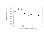
表1に粉砕粉末のD50の測定結果を示す。また、図1にBサイト原料粉末(TiO2粉末)のBET値と粉砕粉末のD50の関係を示している。表1及び図1より、BET値を20m2/g以上にすることにより、粉砕粉末のD50を1.0μm以下、さらには0.8μm以下にできることがわかる。このことは、同一の粉砕時間でより微細な誘電体粉末を得ることができることを示しており、本発明によれば、粉砕による歪が少なく誘電特性の高い微細な誘電体粉末を原料とする誘電体磁器組成物が得られることを示唆している。 Table 1 shows the measurement results of D50 of the pulverized powder. FIG. 1 shows the relationship between the BET value of the B-site raw material powder (TiO 2 powder) and D50 of the pulverized powder. It can be seen from Table 1 and FIG. 1 that by setting the BET value to 20 m 2 / g or more, the D50 of the pulverized powder can be 1.0 μm or less, and further 0.8 μm or less. This indicates that a finer dielectric powder can be obtained with the same pulverization time. According to the present invention, a dielectric powder made from a fine dielectric powder with less distortion caused by pulverization and high dielectric properties is used. This suggests that a body porcelain composition can be obtained.
次に、9種類の粉砕粉末100モルに対して以下の副成分の粉末を添加した後に、ボールミルにより湿式混合した。ボールミルとして、4寸ポット及びメディアとしてZrO2ボール(φ10mm:200g、φ3mm:430g)を用い、120rpmで16時間処理した。また、ポットには粉砕粉末を100g投入し、スラリー濃度を33%とした。さらに、混合に先立ち、分散剤(東亞合成(株)製:A−30SL)を0.2wt%添加した。
MnO(D50=0.55μm):0.365モル
V2O5(D50=0.52μm):0.1モル
Y2O3(D50=0.33μm):0.035モル
CaSiO3(D50=1.178μm):1.616モル
Next, after adding the powder of the following subcomponents to 100 mols of nine kinds of pulverized powders, wet mixing was performed by a ball mill. Using a 4-inch pot as a ball mill and ZrO 2 balls (φ10 mm: 200 g, φ3 mm: 430 g) as media, treatment was performed at 120 rpm for 16 hours. Further, 100 g of the pulverized powder was put into the pot, and the slurry concentration was set to 33%. Further, prior to mixing, 0.2 wt% of a dispersant (manufactured by Toagosei Co., Ltd .: A-30SL) was added.
MnO (D50 = 0.55 μm): 0.365 mol V 2 O 5 (D50 = 0.52 μm): 0.1 mol Y 2 O 3 (D50 = 0.33 μm): 0.035 mol CaSiO 3 (D50 = 1.178 μm): 1.616 mol
ボールミルによる湿式混合が終了した後に、乾燥機を用いて120℃の温度下で24時間保持して乾燥した。
乾燥された混合粉末30gに対して、バインダとして東レ(株)製のAQナイロンP−70の15%水溶液を固形分で2.5wt%(5g)を添加した後に、100℃で90分間乾燥して造粒した。
この造粒粉を、1ton/cm2の圧力で加圧成形してφ12mm×t6.2mmの成形体を得た。次いでこの成形体を、650℃で2時間保持する脱バインダを行った後に、1350℃まで昇温した後に4時間保持することにより焼成を行った。なお、脱バインダ及び焼成は大気フロー中で行った。また、脱バインダ、焼成における昇温速度は200℃/hr.である。
After the wet mixing by the ball mill was completed, it was dried using a drier at a temperature of 120 ° C. for 24 hours.
After adding 2.5 wt% (5 g) of 15% aqueous solution of AQ nylon P-70 manufactured by Toray Industries, Ltd. as a binder to 30 g of the dried mixed powder, it was dried at 100 ° C. for 90 minutes. And granulated.
This granulated powder was pressure-molded at a pressure of 1 ton / cm 2 to obtain a molded body of φ12 mm × t6.2 mm. Next, the molded body was debindered by holding at 650 ° C. for 2 hours, then heated to 1350 ° C. and then held for 4 hours to be fired. The binder removal and firing were performed in an atmospheric flow. Moreover, the temperature increase rate in binder removal and baking is 200 ° C./hr.
以上で得られた誘電体磁器組成物について、比誘電率(εr)とQfを誘電体共振器法(n=2)により測定した。その結果を表1に示す。なお、測定には、RFベクトルネットワークアナライザ(横川ヒューレットパッカード(株)製:HP8510)を用いた。また、測定に当たって、誘電体磁器組成物は厚さが5±0.5mmの試料に研磨加工された。 The dielectric ceramic composition obtained above was measured for dielectric constant (εr) and Qf by the dielectric resonator method (n = 2). The results are shown in Table 1. For the measurement, an RF vector network analyzer (manufactured by Yokogawa Hewlett-Packard Co., Ltd .: HP8510) was used. In measurement, the dielectric ceramic composition was polished into a sample having a thickness of 5 ± 0.5 mm.
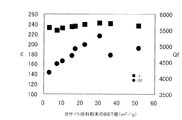
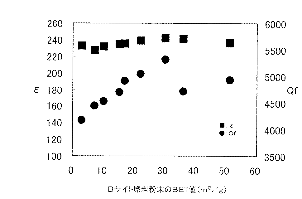
図2にBサイト原料粉末のBET値と、得られた誘電体磁器組成物の比誘電率(εr)及びQfとの関係を示す。図2に示すように、Bサイト原料粉末のBET値が大きくなるにつれて誘電体磁器組成物の比誘電率(εr)及びQfが大きくなる。しかし、BET値が30m2/gをピークに、誘電体磁器組成物の比誘電率(εr)及びQfが低下する傾向にある。この結果より、本発明では、Bサイト原料粉末のBET値を20〜40m2/g、望ましくは25〜35m2/gの範囲とする。 FIG. 2 shows the relationship between the BET value of the B-site raw material powder and the relative dielectric constant (εr) and Qf of the obtained dielectric ceramic composition. As shown in FIG. 2, the dielectric constant (εr) and Qf of the dielectric ceramic composition increase as the BET value of the B-site raw material powder increases. However, when the BET value peaks at 30 m 2 / g, the dielectric constant (εr) and Qf of the dielectric ceramic composition tend to decrease. From this result, in the present invention, the BET value of the B-site raw material powder is set to a range of 20 to 40 m 2 / g, desirably 25 to 35 m 2 / g.
Claims (3)
Aサイトを構成するAサイト原料粉末とBサイトを構成するBET値が20〜40m2/gのBサイト原料粉末とを含む混合物を仮焼して仮焼物を得る仮焼工程と、
前記仮焼物を粉砕して粉砕粉末を得る粉砕工程と、
所定の処理が施された前記粉砕粉末を所定条件で加熱保持して焼成物を得る焼成工程と、を備えることを特徴とする誘電体磁器組成物の製造方法。 A method for producing a dielectric ceramic composition comprising a perovskite oxide having an ABO 3 type atomic arrangement,
A calcining step of calcining a mixture containing the A site raw material powder constituting the A site and the B site raw material powder having a BET value of 20 to 40 m 2 / g constituting the B site;
A pulverization step of pulverizing the calcined product to obtain a pulverized powder;
And a firing step of obtaining a fired product by heating and holding the pulverized powder subjected to a predetermined treatment under a predetermined condition.
Priority Applications (1)
| Application Number | Priority Date | Filing Date | Title |
|---|---|---|---|
| JP2004037581A JP2005225735A (en) | 2004-02-16 | 2004-02-16 | Production method for dielectric porcelain composition |
Applications Claiming Priority (1)
| Application Number | Priority Date | Filing Date | Title |
|---|---|---|---|
| JP2004037581A JP2005225735A (en) | 2004-02-16 | 2004-02-16 | Production method for dielectric porcelain composition |
Publications (1)
| Publication Number | Publication Date |
|---|---|
| JP2005225735A true JP2005225735A (en) | 2005-08-25 |
Family
ID=35000742
Family Applications (1)
| Application Number | Title | Priority Date | Filing Date |
|---|---|---|---|
| JP2004037581A Withdrawn JP2005225735A (en) | 2004-02-16 | 2004-02-16 | Production method for dielectric porcelain composition |
Country Status (1)
| Country | Link |
|---|---|
| JP (1) | JP2005225735A (en) |
Cited By (8)
| Publication number | Priority date | Publication date | Assignee | Title |
|---|---|---|---|---|
| JP2007290944A (en) * | 2006-03-27 | 2007-11-08 | Kyocera Corp | Barium calcium titanate powder and production method thereof |
| WO2009001690A1 (en) * | 2007-06-27 | 2008-12-31 | Murata Manufacturing Co., Ltd. | Semiconductor ceramic powder, semiconductor ceramic, and laminated semiconductor capacitor |
| DE112008002498T5 (en) | 2007-09-26 | 2010-08-05 | Universal Entertainment Corporation | Process for the preparation of a complex metal oxide powder |
| DE112008002499T5 (en) | 2007-09-26 | 2010-09-02 | Universal Entertainment Corporation | Process for producing a sintered body of a complex metal oxide |
| US8232333B2 (en) * | 2005-11-04 | 2012-07-31 | Evonik Degussa Gmbh | Process for producing ultrafine powders based on polyamides, ultrafine polyamide powders and their use |
| KR101249000B1 (en) * | 2012-10-10 | 2013-04-02 | 한국지질자원연구원 | Production of mixed powder of carbide and carbonitride for cermet, and cermet therefrom |
| KR101248996B1 (en) * | 2012-10-10 | 2013-04-02 | 한국지질자원연구원 | Production of carbide and carbonitride powders containing binder, and cermet therefrom |
| CN120157471A (en) * | 2025-04-09 | 2025-06-17 | 清华大学 | A calcium titanate-based ceramic with high dielectric constant and low dielectric loss and its preparation method and application |
-
2004
- 2004-02-16 JP JP2004037581A patent/JP2005225735A/en not_active Withdrawn
Cited By (12)
| Publication number | Priority date | Publication date | Assignee | Title |
|---|---|---|---|---|
| US8232333B2 (en) * | 2005-11-04 | 2012-07-31 | Evonik Degussa Gmbh | Process for producing ultrafine powders based on polyamides, ultrafine polyamide powders and their use |
| JP2007290944A (en) * | 2006-03-27 | 2007-11-08 | Kyocera Corp | Barium calcium titanate powder and production method thereof |
| WO2009001690A1 (en) * | 2007-06-27 | 2008-12-31 | Murata Manufacturing Co., Ltd. | Semiconductor ceramic powder, semiconductor ceramic, and laminated semiconductor capacitor |
| US8040658B2 (en) | 2007-06-27 | 2011-10-18 | Murata Manufacturing Co., Ltd. | Semiconductor ceramic powder, semiconductor ceramic, and monolithic semiconductor ceramic capacitor |
| JP5347961B2 (en) * | 2007-06-27 | 2013-11-20 | 株式会社村田製作所 | Semiconductor ceramic powder, semiconductor ceramic, and multilayer semiconductor ceramic capacitor |
| DE112008002498T5 (en) | 2007-09-26 | 2010-08-05 | Universal Entertainment Corporation | Process for the preparation of a complex metal oxide powder |
| DE112008002499T5 (en) | 2007-09-26 | 2010-09-02 | Universal Entertainment Corporation | Process for producing a sintered body of a complex metal oxide |
| KR101249000B1 (en) * | 2012-10-10 | 2013-04-02 | 한국지질자원연구원 | Production of mixed powder of carbide and carbonitride for cermet, and cermet therefrom |
| KR101248996B1 (en) * | 2012-10-10 | 2013-04-02 | 한국지질자원연구원 | Production of carbide and carbonitride powders containing binder, and cermet therefrom |
| US9238854B2 (en) | 2012-10-10 | 2016-01-19 | Korea Institute Of Geoscience And Mineral Resources | Method of producing carbide and carbon nitride powders containing binder, and cermet obtained from the same |
| CN120157471A (en) * | 2025-04-09 | 2025-06-17 | 清华大学 | A calcium titanate-based ceramic with high dielectric constant and low dielectric loss and its preparation method and application |
| CN120157471B (en) * | 2025-04-09 | 2025-11-18 | 清华大学 | High-dielectric-constant low-dielectric-loss calcium titanate-based ceramic and preparation method and application thereof |
Similar Documents
| Publication | Publication Date | Title |
|---|---|---|
| US20180131065A1 (en) | Radiofrequency and other electronic devices formed from enhanced resonant frequency hexaferrite materials | |
| US11069983B2 (en) | Modified Z-type hexagonal ferrite materials with enhanced resonant frequency | |
| JP2005225735A (en) | Production method for dielectric porcelain composition | |
| CN102264668A (en) | Dielectric ceramic, dielectric resonator utilizing same, and method for manufacturing dielectric ceramic | |
| CN101186495A (en) | Microwave dielectric composition and microwave dielectric resonator | |
| JP3559434B2 (en) | Method for producing dielectric porcelain composition | |
| JP2005200232A (en) | Dielectric ceramic composition | |
| JP2010100511A (en) | Composite sintered compact of magnetic substance and dielectric substance, and lc composite electronic component | |
| JP2002167281A (en) | Dielectric powder, method for producing the same, sintered body and capacitor using the same | |
| WO1996008019A1 (en) | Dielectric procelain composition and its manufacture | |
| JP4465663B2 (en) | Dielectric porcelain composition | |
| JP2004091266A (en) | Gallium-added dielectric porcelain composition, dielectric resonator, and microwave communication apparatus | |
| JP2005225721A (en) | Production method for dielectric powder and production method for composite dielectric material | |
| JP4419889B2 (en) | Dielectric porcelain composition | |
| JP5566183B2 (en) | Dielectric powder and sintered body and capacitor using the same | |
| JP2003146752A (en) | Dielectric porcelain composition | |
| JPWO2006013981A1 (en) | Dielectric ceramic composition and dielectric ceramic | |
| JP6064315B2 (en) | Magnetic oxide sintered body, and antenna and wireless communication device using the same | |
| JP2007045690A (en) | Dielectric porcelain composition | |
| JP6064732B2 (en) | Magnetic oxide sintered body and high-frequency magnetic component using the same | |
| JP2007063076A (en) | Dielectric ceramic composition | |
| JP2008088004A (en) | Method of manufacturing dielectric porcelain composition | |
| JP2006256931A (en) | Dielectric porcelain composition | |
| JP4383951B2 (en) | High frequency dielectric ceramic composition and method for producing the same | |
| JP4505795B2 (en) | Method for producing dielectric ceramic composition for electronic device |
Legal Events
| Date | Code | Title | Description |
|---|---|---|---|
| A621 | Written request for application examination |
Free format text: JAPANESE INTERMEDIATE CODE: A621 Effective date: 20061205 |
|
| A761 | Written withdrawal of application |
Free format text: JAPANESE INTERMEDIATE CODE: A761 Effective date: 20090304 |