JP2005225721A - Production method for dielectric powder and production method for composite dielectric material - Google Patents
Production method for dielectric powder and production method for composite dielectric material Download PDFInfo
- Publication number
- JP2005225721A JP2005225721A JP2004036612A JP2004036612A JP2005225721A JP 2005225721 A JP2005225721 A JP 2005225721A JP 2004036612 A JP2004036612 A JP 2004036612A JP 2004036612 A JP2004036612 A JP 2004036612A JP 2005225721 A JP2005225721 A JP 2005225721A
- Authority
- JP
- Japan
- Prior art keywords
- powder
- dielectric
- site
- raw material
- producing
- Prior art date
- Legal status (The legal status is an assumption and is not a legal conclusion. Google has not performed a legal analysis and makes no representation as to the accuracy of the status listed.)
- Withdrawn
Links
Images
Landscapes
- Inorganic Compounds Of Heavy Metals (AREA)
- Compositions Of Macromolecular Compounds (AREA)
- Inorganic Insulating Materials (AREA)
- Compositions Of Oxide Ceramics (AREA)
Abstract
Description
本発明は、誘電体粉末に関し、特に樹脂とともに複合誘電体材料を形成して高い誘電特性を得ることのできる誘電体粉末の製造方法及び複合誘電体材料の製造方法に関するものである。 The present invention relates to a dielectric powder, and more particularly, to a dielectric powder manufacturing method and a composite dielectric material manufacturing method capable of obtaining a high dielectric property by forming a composite dielectric material together with a resin.
近年、通信機の小型化、軽量化、高速化が強く望まれている。その中で、デジタル携帯電話等の携帯移動体通信、衛星通信に使用される電波の周波数帯域はメガからギガHz帯(「GHz帯」という)の高周波帯域のものが使用されている。使用される通信機器の急速な発展の中で、匡体及び基板、電子素子の小型高密度実装化が図られているが、高周波帯域に対応した通信機器の小型化、軽量化をより一層推進するためには、通信機器に使用される基板等の材料はGHz帯において高周波伝送特性が優れた(誘電損失が小さい)ものでなければならない。ここで、誘電損失は周波数と基板の比誘電率εrと誘電正接(以下tanδと記載する)の積に比例する。よって、誘電損失を小さくするためには基板のtanδを小さくしなければならない。また、基板中では電磁波の波長が1/(εr)0.5に短縮されるため、比誘電率εrが大きい程基板の小型化が可能である。以上のことから高周波帯域で使用される小型の通信機器、電子機器、情報機器に用いる回路基板としては、比誘電率εrが高く、かつQf(品質係数Q=1/tanδ、f=共振周波数)が大きいことが要求されている。 In recent years, miniaturization, weight reduction, and speeding up of communication devices have been strongly desired. Among them, the frequency band of radio waves used for portable mobile communications such as digital cellular phones and satellite communications is in the high frequency band of mega to giga Hz band (referred to as “GHz band”). Amid the rapid development of used communication equipment, the housing, board, and electronic elements have been miniaturized and densely mounted. However, the communication equipment that supports the high frequency band has been further reduced in size and weight. In order to achieve this, materials such as substrates used in communication equipment must be excellent in high-frequency transmission characteristics (low dielectric loss) in the GHz band. Here, the dielectric loss is proportional to the product of the frequency, the relative dielectric constant εr of the substrate, and the dielectric loss tangent (hereinafter referred to as tan δ). Therefore, in order to reduce the dielectric loss, tan δ of the substrate must be reduced. Further, since the wavelength of the electromagnetic wave in the substrate is shortened to 1 / (εr) 0.5 , the substrate can be downsized as the relative dielectric constant εr increases. As described above, a circuit board used for a small communication device, electronic device, or information device used in a high frequency band has a high relative dielectric constant εr and Qf (quality factor Q = 1 / tan δ, f = resonance frequency). Is required to be large.
このような回路基板の材料としては、無機材料としての誘電体材料(焼成体)、有機材料としてのフッ素樹脂等が用いられている。ところが、誘電体材料からなる基板は、寸法精度、加工性に難点があり、脆いため欠けや割れが生じやすいという問題点があった。他方、樹脂等の有機材料からなる基板は、成形性及び加工性に優れるという利点はあるが、比誘電率εrが小さいという問題があった。このため、近年、両者の利点を有する基板として、例えば特許文献1(特開2003−128930号公報)、特許文献2(特開2003−151352号)において誘電体粉末と樹脂材料とからなる複合基板が開示されている。 As such a circuit board material, a dielectric material (fired body) as an inorganic material, a fluororesin as an organic material, or the like is used. However, a substrate made of a dielectric material has problems in dimensional accuracy and workability, and is fragile, so that there is a problem that chips and cracks are likely to occur. On the other hand, a substrate made of an organic material such as a resin has the advantage of being excellent in moldability and workability, but has a problem that the relative dielectric constant εr is small. Therefore, in recent years, as a substrate having both advantages, for example, a composite substrate made of a dielectric powder and a resin material in Patent Document 1 (Japanese Patent Laid-Open No. 2003-128930) and Patent Document 2 (Japanese Patent Laid-Open No. 2003-151352). Is disclosed.
誘電体材料としては、チタン酸バリウム、チタン酸ジルコン酸鉛等のABO3型の原子配列を持つペロブスカイト酸化物が通常用いられており、その粉末(誘電体粉末)の製造方法としては、液相法、気相法、フラックス法及び固相法が知られている。
液相法は、金属塩の水溶液あるいは有機溶媒溶液を出発原料として、水和物等の金属酸化物前駆体粉末を製造し、次いでこの前駆体粉末を焼成して2種類以上の金属元素を含む金属酸化物粉末を製造する方法である。液相法としては、沈殿法、共沈法、加水分解法等が知られている。
気相法は、金属蒸気あるいは金属化合物の気相状態での化学反応により金属酸化物粉末を製造する方法であり、粒度分布が狭く、凝集が少ない粉末が得られる利点がある。
フラックス法は、金属酸化物の混合粉末にフラックス成分を添加して焼成することにより金属酸化物粉末を製造する方法である。
As the dielectric material, a perovskite oxide having an ABO 3 type atomic arrangement such as barium titanate and lead zirconate titanate is usually used, and a method for producing the powder (dielectric powder) is a liquid phase. Methods, gas phase methods, flux methods and solid phase methods are known.
In the liquid phase method, a metal oxide precursor powder such as a hydrate is produced using a metal salt aqueous solution or an organic solvent solution as a starting material, and then the precursor powder is fired to contain two or more kinds of metal elements. This is a method for producing a metal oxide powder. As the liquid phase method, a precipitation method, a coprecipitation method, a hydrolysis method and the like are known.
The gas phase method is a method for producing a metal oxide powder by a chemical reaction of a metal vapor or a metal compound in a gas phase state, and has an advantage that a powder having a narrow particle size distribution and less aggregation is obtained.
The flux method is a method for producing a metal oxide powder by adding a flux component to a metal oxide mixed powder and firing it.
以上の液相法、気相法及びフラックス法により得られる誘電体粉末は、その粒径を微細とすることができるとともに粒度分布を狭くできるという利点がある。ここで、上述した複合基板を作製する場合、樹脂材料と混合される誘電体粉末は、複合基板が積層された際の層間を薄くする場合、その粒径が小さいことが望まれる。液相法、気相法及びフラックス法により得られる誘電体粉末は、その粒径が微細であるため、複合基板を作製する上で望ましい誘電体粉末の製造方法である。しかし、これらの方法により得られる誘電体粉末のコストが高いという問題がある。 The dielectric powder obtained by the above liquid phase method, gas phase method and flux method has the advantage that the particle size can be made fine and the particle size distribution can be narrowed. Here, when the composite substrate described above is manufactured, it is desirable that the dielectric powder mixed with the resin material has a small particle diameter when the interlayer when the composite substrate is laminated is thinned. Since the dielectric powder obtained by the liquid phase method, the gas phase method and the flux method has a fine particle size, it is a desirable method for producing a dielectric powder in producing a composite substrate. However, there is a problem that the cost of the dielectric powder obtained by these methods is high.
以上の方法に比べて低コストで誘電体粉末を得る方法として固相法が知られている。固相法は、金属酸化物、炭酸塩等の粉末を高温で焼成し、得られた焼成物を粉砕するという工程を備えている。例えば、チタン酸バリウムを得ようという場合、TiO2粉末とBaCO3粉末を原料粉末として混合、焼成し、得られた焼成物を粉砕する。この粉砕過程で、粉砕された粉末には歪が発生するため、誘電特性を劣化させてしまう。特に、粉砕により粒径の小さな粉末を得るためには、粉砕時間を長くするあるいは粉砕条件を厳しくする必要があり、微細な誘電体粉末は誘電特性が著しく劣化してしまう。誘電特性を劣化させないために粉砕時間を短くすると、微細な誘電体粉末を得ることができない。したがって、これまでは、固相法による誘電体粉末を用いた複合基板は所望する特性を得がたいという問題があった。一方で、固相法によって、誘電特性の劣化が少ない微細な粉末が得られれば、コスト的な点も含めて考えると、複合基板を得るために非常に望ましい誘電体粉末の製造方法になる。 A solid phase method is known as a method for obtaining dielectric powder at a lower cost than the above methods. The solid phase method includes a step of firing a powder such as a metal oxide or carbonate at a high temperature and pulverizing the obtained fired product. For example, when obtaining barium titanate, TiO 2 powder and BaCO 3 powder are mixed and fired as raw material powder, and the fired product obtained is pulverized. In this pulverization process, distortion occurs in the pulverized powder, which deteriorates the dielectric characteristics. In particular, in order to obtain a powder having a small particle diameter by pulverization, it is necessary to lengthen the pulverization time or to make the pulverization conditions strict, and the dielectric characteristics of the fine dielectric powder are significantly deteriorated. If the pulverization time is shortened in order not to deteriorate the dielectric characteristics, it is impossible to obtain a fine dielectric powder. Therefore, until now, there has been a problem that a composite substrate using a dielectric powder by a solid phase method cannot obtain desired characteristics. On the other hand, if a fine powder with little deterioration in dielectric properties can be obtained by the solid phase method, it becomes a very desirable method for producing a dielectric powder in order to obtain a composite substrate, considering the cost.
本発明は以上の背景に鑑み、固相法を用いながらも、誘電特性の劣化が抑制された微細な誘電体粉末を製造する方法を提供することを課題とする。また、本発明はそのような誘電体粉末を用いて、誘電特性の優れた、誘電体粉末と樹脂材料とからなる複合誘電体材料の製造方法の提供を課題とする。 In view of the above background, an object of the present invention is to provide a method for producing a fine dielectric powder in which deterioration of dielectric properties is suppressed while using a solid phase method. Another object of the present invention is to provide a method for producing a composite dielectric material composed of a dielectric powder and a resin material, using such a dielectric powder and having excellent dielectric characteristics.
本発明が対象とするABO3型の原子配列を持つペロブスカイト酸化物を含む誘電体材料は、Aサイトを構成するためのAサイト原料とBサイトを構成するためのBサイト原料とを混合、焼成することにより得ることができる。例えば、(Sr,Ca)TiO3を得ようとする場合には、通常、Aサイト原料としてSrCO3粉末及びCaCO3粉末、Bサイト原料としてTiO2粉末を用意する。本発明者らの検討によれば、Bサイト原料のBET値を特定の値に制御することにより、焼成後の粉砕を軽微にしても十分に微細な粉末が得られることが判明した。そして、この粉末を用いた複合誘電体材料として優れた誘電特性を備えることが確認された。 A dielectric material containing a perovskite oxide having an ABO 3 type atomic arrangement targeted by the present invention is obtained by mixing and firing an A site material for forming the A site and a B site material for forming the B site. Can be obtained. For example, in order to obtain (Sr, Ca) TiO 3 , SrCO 3 powder and CaCO 3 powder are usually prepared as the A site material, and TiO 2 powder is prepared as the B site material. According to the study by the present inventors, it has been found that by controlling the BET value of the B site raw material to a specific value, a sufficiently fine powder can be obtained even if the pulverization after firing is light. And it was confirmed that the composite dielectric material using this powder has excellent dielectric properties.
本発明は以上の知見に基づくものであり、ABO3型の原子配列を持つペロブスカイト酸化物を含む誘電体粉末の製造方法であって、Aサイトを構成するAサイト原料粉末とBサイトを構成する比表面積(BET法による値、本願発明において単にBET値と記す)が20m2/g以上のBサイト原料粉末とを含む混合物を得る工程と、混合物を焼成して第1焼成物を得る第1焼成工程と、第1焼成物を粉砕して第1粉末を得る第1粉砕工程と、を備えることを特徴としている。以上の本発明による第1粉末は、BET値が20m2/g以上であるBサイト原料粉末を用いているため、長時間の粉砕を経ることなく、微細、具体的には1μm以下、さらには0.8μm以下のD50(累積個数が50%となる粒子の粒径)とすることができる。この第1粉末は、長時間の粉砕を経なくてもよいから、粉砕による歪の発生が少なく、優れた誘電特性を発揮することができる。
本発明は、第1粉砕工程で得られた第1粉末に所定の処理を施した後に焼成して第2焼成物を得る第2焼成工程と、第2焼成物を粉砕して第2粉末を得る第2粉砕工程と、を備えることができる。この第2粉末もまた、第1粉末と同様に、長時間の粉砕を経ることなく、D50が1μm以下の微細なものとすることができる。なお、所定の処理とは、種々の副成分を添加、混合することを含む概念である。ただし、この副成分は、第1焼成工程前に添加することもできる。
The present invention is based on the above knowledge, and is a method for producing a dielectric powder containing a perovskite oxide having an ABO 3 type atomic arrangement, which comprises an A site raw material powder that constitutes the A site and a B site. A step of obtaining a mixture containing a B-site raw material powder having a specific surface area (value according to the BET method, simply referred to as BET value in the present invention) of 20 m 2 / g, and a first firing product obtained by firing the mixture And a first pulverizing step of pulverizing the first baked product to obtain a first powder. Since the first powder according to the present invention uses the B-site raw material powder having a BET value of 20 m 2 / g or more, it is fine, specifically, 1 μm or less, and without being pulverized for a long time. The D50 can be 0.8 μm or less (the particle diameter of the particles with a cumulative number of 50%). Since the first powder does not need to be pulverized for a long time, the distortion due to the pulverization is small and excellent dielectric properties can be exhibited.
The present invention includes a second firing step for obtaining a second fired product by subjecting the first powder obtained in the first grinding step to a predetermined treatment, and a second powder obtained by grinding the second fired product. Obtaining a second grinding step. Similarly to the first powder, this second powder can be made fine with a D50 of 1 μm or less without being pulverized for a long time. The predetermined treatment is a concept including adding and mixing various subcomponents. However, this subcomponent can also be added before the first firing step.
本発明にかかる誘電体粉末は、AサイトがBa、Ca及びSrから選択される1種又は2種以上の原子を含み、BサイトがTi、Zr及びNbから選択される1種又は2種以上の原子を含むことが誘電特性の点から望ましい。 In the dielectric powder according to the present invention, the A site contains one or more atoms selected from Ba, Ca and Sr, and the B site is selected from one or more selected from Ti, Zr and Nb. From the viewpoint of dielectric properties, it is desirable to contain the above atoms.
本発明による誘電体粉末は、ABO3型の原子配列を持つペロブスカイト酸化物からなる誘電体粉末と樹脂とを含む複合誘電体材料の製造に用いることができる。つまり本発明は、Aサイトを構成するAサイト原料粉末とBサイトを構成するBET値が20〜40m2/gのBサイト原料粉末とを原料とする焼成物を粉砕して誘電体粉末を得る工程と、この誘電体粉末と樹脂を複合化する工程と、を備えることを特徴とする複合誘電体材料の製造方法を提供する。
本発明の複合誘電体材料の製造方法は、BET値が20〜40m2/gであるBサイト原料粉末に基づく焼成物を粉砕して得た誘電体粉末を使用するため、得られる複合誘電体材料の誘電特性は良好である。
ここで、Aサイト原料粉末とBET値が20〜40m2/gのBサイト原料粉末とを原料とする焼成物とは、前述した第1焼成物及び第2焼成物の両者を包含している。また、上記誘電体粉末は、第1粉末及び第2粉末の両者を包含している。
The dielectric powder according to the present invention can be used for the production of a composite dielectric material including a dielectric powder made of a perovskite oxide having an ABO 3 type atomic arrangement and a resin. That is, according to the present invention, a dielectric powder is obtained by pulverizing a fired product made from A site raw material powder constituting A site and B site raw material powder having BET value of 20 to 40 m 2 / g constituting B site. There is provided a method for producing a composite dielectric material comprising a step and a step of combining the dielectric powder and a resin.
The method for producing a composite dielectric material of the present invention uses a dielectric powder obtained by pulverizing a fired product based on a B-site raw material powder having a BET value of 20 to 40 m 2 / g. The dielectric properties of the material are good.
Here, the fired product made from the A site raw material powder and the B site raw material powder having a BET value of 20 to 40 m 2 / g includes both the first fired product and the second fired product. . The dielectric powder includes both the first powder and the second powder.
本発明による複合誘電体材料の製造方法においても、AサイトがBa、Ca及びSrから選択される1種又は2種以上の原子を含み、BサイトがTi、Zr及びNbから選択される1種又は2種以上の原子を含むことが望ましい。 Also in the method for producing a composite dielectric material according to the present invention, the A site contains one or more atoms selected from Ba, Ca and Sr, and the B site is selected from Ti, Zr and Nb. Or it is desirable to contain 2 or more types of atoms.
以上説明したように、本発明によれば、長時間の粉砕を経ることなく、微細な誘電体粉末を得ることができる。したがって、低コストでかつ誘電特性の優れた複合誘電体材料を得ることができる。 As described above, according to the present invention, a fine dielectric powder can be obtained without pulverizing for a long time. Therefore, a composite dielectric material having low cost and excellent dielectric characteristics can be obtained.
本発明が適用される誘電体材料は、ABO3型の原子配列を持つペロブスカイト酸化物である。ここで、AサイトがBa、Ca及びSrから選択される1種又は2種以上の原子を含み、さらにBサイトがTi、Zr及びNbから選択される1種又は2種以上の原子を含むことが望ましい。したがって、本発明は少なくとも以下のペロブスカイト酸化物に適用されることが望ましい。
SrTiO3、CaTiO3、(Sr,Ca)TiO3、(Sr,Ba)TiO3、(Ca,Ba)TiO3、(Ba,Sr,Ca)TiO3
SrZrO3、CaZrO3、(Sr,Ca)ZrO3、(Sr,Ba)ZrO3、(Ca,Ba)ZrO3、(Ba,Sr,Ca)ZrO3
SrNbO3、CaNbO3、(Sr,Ca)NbO3、(Sr,Ba)NbO3、(Ca,Ba)NbO3、(Ba,Sr,Ca)NbO3
Sr(Ti,Zr)O3、Ca(Ti,Nb)O3、(Sr,Ca)(Zr,Nb)O3、(Sr,Ba)(Ti,Zr,Nb)O3
The dielectric material to which the present invention is applied is a perovskite oxide having an ABO 3 type atomic arrangement. Here, the A site contains one or more atoms selected from Ba, Ca and Sr, and the B site contains one or more atoms selected from Ti, Zr and Nb. Is desirable. Therefore, the present invention is desirably applied to at least the following perovskite oxides.
SrTiO 3 , CaTiO 3 , (Sr, Ca) TiO 3 , (Sr, Ba) TiO 3 , (Ca, Ba) TiO 3 , (Ba, Sr, Ca) TiO 3
SrZrO 3 , CaZrO 3 , (Sr, Ca) ZrO 3 , (Sr, Ba) ZrO 3 , (Ca, Ba) ZrO 3 , (Ba, Sr, Ca) ZrO 3
SrNbO 3 , CaNbO 3 , (Sr, Ca) NbO 3 , (Sr, Ba) NbO 3 , (Ca, Ba) NbO 3 , (Ba, Sr, Ca) NbO 3
Sr (Ti, Zr) O 3 , Ca (Ti, Nb) O 3 , (Sr, Ca) (Zr, Nb) O 3 , (Sr, Ba) (Ti, Zr, Nb) O 3
本発明が適用される誘電体材料は、上述したペロブスカイト酸化物を主成分とし、さらに種々の副成分を含有することができる。本発明においては、A(ただし、AはNi、Mn及びCrから選択される1種又は2種の元素)の酸化物を副成分として添加することができる。また、X(ただし、XはV、Nb、W、Ta及びMoから選択される1種又は2種以上の元素)の酸化物を副成分として添加することができる。さらに、R(ただし、RはSc、Y、La、Ce、Pr、Nd、Pm、Sm、Eu、Gd、Tb、 Dy、Ho、Er、Tm、Yb及びLuから選択される1種又は2種以上の元素)の酸化物を添加することができる。さらにまた、SiO2 、MO(ただし、MはBa、Ca、Sr及びMgから選択される1種又は2種以上の元素)、Li2O、B2O3及びMSiO3から選択される1種又は2種以上の化合物を添加することができる。 The dielectric material to which the present invention is applied is based on the perovskite oxide described above, and can further contain various subcomponents. In the present invention, an oxide of A (where A is one or two elements selected from Ni, Mn and Cr) can be added as a subcomponent. In addition, an oxide of X (where X is one or more elements selected from V, Nb, W, Ta, and Mo) can be added as a subcomponent. Further, R (where R is Sc, Y, La, Ce, Pr, Nd, Pm, Sm, Eu, Gd, Tb, Dy, Ho, Er, Tm, Yb and Lu are selected from one or two kinds Oxides of the above elements) can be added. Furthermore, SiO 2 , MO (where M is one or more elements selected from Ba, Ca, Sr and Mg), Li 2 O, B 2 O 3 and one kind selected from MSiO 3. Alternatively, two or more compounds can be added.
本発明は、上述したABO3型の原子配列を持つペロブスカイト酸化物からなる誘電体粉末を製造する方法である。ところで、焼成体からなる誘電体材料は、例えば最終組成になるように秤量された原料粉末を混合する工程、混合粉末を仮焼する工程、仮焼物を粉砕する工程、粉砕粉末を焼成する工程を経ることにより製造することができる。この製造方法において、誘電体粉末は、上述の仮焼物を粉砕することにより得ることができるし、焼成工程を経て得られた焼成体を粉砕することにより得ることもできる。前者の態様を第1態様、後者の態様を第2態様とすると、本発明における誘電体粉末の製造方法は、第1態様又は第2態様のいずれについても適用することができる。そして、本発明における粉末の粒径制御の効果は、第1態様、つまり仮焼後の粉砕粉末において具現されるとともに、第2態様、つまり焼成体を粉砕して得られる粉末にも具現される。なお、第1態様の場合、通常仮焼と称されている工程の後に焼成が行われないため、本発明においては、これを仮焼と呼ばずに第1焼成と呼び、第2態様において、第1焼成の後に行われる焼成を第2焼成ということにする。 The present invention is a method for producing a dielectric powder made of the perovskite oxide having the ABO 3 type atomic arrangement described above. By the way, the dielectric material made of a fired body includes, for example, a step of mixing raw material powders weighed so as to have a final composition, a step of calcining the mixed powder, a step of grinding the calcined product, and a step of firing the ground powder. It can manufacture by passing. In this manufacturing method, the dielectric powder can be obtained by pulverizing the above-mentioned calcined product, and can also be obtained by pulverizing the fired body obtained through the firing step. When the former mode is the first mode and the latter mode is the second mode, the method for producing a dielectric powder in the present invention can be applied to either the first mode or the second mode. The effect of controlling the particle size of the powder in the present invention is embodied in the first aspect, that is, the pulverized powder after calcining, and also in the second aspect, that is, the powder obtained by pulverizing the fired body. . In the case of the first aspect, since the baking is not performed after the step usually referred to as calcination, in the present invention, this is referred to as the first calcination instead of calcination, and in the second aspect, The firing performed after the first firing is referred to as the second firing.
はじめに第1態様について説明する。
本発明の誘電体粉末を得るための原料には、主成分を構成する原料と、副成分を構成する原料とが用意される。ただし、副成分の添加は望ましいが、本発明において必須のものではない。
主成分を構成する原料としては、Aサイトを構成するためのAサイト原料粉末及びBサイトを構成するためのBサイト原料粉末が用意される。Aサイト原料粉末及びBサイト原料粉末としては、当該元素の酸化物及び/又は焼成により酸化物になる化合物が用いられる。焼成により酸化物になる化合物としては、例えば炭酸塩、硝酸塩、シュウ酸塩、有機金属化合物等が挙げられる。これらの化合物と酸化物とを併用してもよい。具体的には、Aサイト原料粉末としては、SrCO3粉末、CaCO3粉末及びBaCO3粉末から選択される1種又は2種以上を用いるのが望ましい。また、Bサイト原料粉末としては、TiO2粉末、ZrO2粉末及びNbO2粉末から選択される1種又は2種以上を用いるのが望ましい。
First, the first aspect will be described.
As the raw material for obtaining the dielectric powder of the present invention, a raw material constituting the main component and a raw material constituting the subcomponent are prepared. However, although the addition of subcomponents is desirable, it is not essential in the present invention.
As the raw material constituting the main component, an A site raw material powder for constituting the A site and a B site raw material powder for constituting the B site are prepared. As the A-site raw material powder and the B-site raw material powder, an oxide of the element and / or a compound that becomes an oxide by firing is used. Examples of the compounds that become oxides upon firing include carbonates, nitrates, oxalates, and organometallic compounds. These compounds and oxides may be used in combination. Specifically, as the A-site raw material powder, it is desirable to use one or more selected from SrCO 3 powder, CaCO 3 powder and BaCO 3 powder. As the B-site material powder, TiO 2 powder, to use one or two or more kinds selected from ZrO 2 powder and NbO 2 powder desirable.
本発明は、比表面積(BET法による値、以下単にBET値と記す)が20m2/g以上のBサイト原料粉末を用いる点に特徴がある。これは、後述する実施例で示しているように、Bサイト原料粉末のBET値が20m2/g以上になると、第1焼成後に長時間の粉砕を行うことなくD50が1μm以下という微細な誘電体粉末を得ることができるからである。長時間の粉砕を行わずに済むため、本発明により得られる誘電体粉末の誘電特性は良好である。結果として、この誘電体粉末を用いた複合誘電体材料の誘電特性も良好である。
一方、本発明において、Aサイト原料粉末は、Bサイト原料粉末のようにBET値を特定することを必要としない。本発明者の検討によると、Aサイト原料粉末のBET値は得られる誘電体粉末の粒径に影響を与えないからである。したがって、Aサイト原料については、D50を0.01〜5.0μmの範囲で適宜選択すればよい。
The present invention is characterized in that a B-site raw material powder having a specific surface area (value according to BET method, hereinafter simply referred to as BET value) of 20 m 2 / g or more is used. As shown in the examples described later, when the BET raw material powder has a BET value of 20 m 2 / g or more, a fine dielectric having a D50 of 1 μm or less without pulverization for a long time after the first firing. This is because body powder can be obtained. Since it is not necessary to grind for a long time, the dielectric characteristics of the dielectric powder obtained by the present invention are good. As a result, the dielectric characteristics of the composite dielectric material using this dielectric powder are also good.
On the other hand, in the present invention, the A-site raw material powder does not need to specify the BET value unlike the B-site raw material powder. According to the study by the present inventor, the BET value of the A-site raw material powder does not affect the particle size of the obtained dielectric powder. Therefore, for the A-site raw material, D50 may be appropriately selected within the range of 0.01 to 5.0 μm.
副成分を構成する副成分原料については以下の通りである。
Aの酸化物については、Aの酸化物及び/又は焼成によりAの酸化物になる化合物を原料として用いることができる。
Xの酸化物については、Xの酸化物及び/又は焼成によりXの酸化物になる化合物から選択される1種類以上の単一酸化物又は複合酸化物を原料として用いることができる。
Rの酸化物については、Rの酸化物及び/又は焼成により酸化物になる化合物から選択される1種類以上の単一酸化物又は複合酸化物を原料として用いることができる。
SiO2 、MO(ただし、Mは、Ba、Ca、Sr及びMgから選択される1種又は2種以上の元素)、Li2O、B2O3及びMSiO3から選択される1種又は2種以上については、当該化合物を原料として用いることができる。
副成分原料粉末も、D50を0.01〜5.0μmの範囲で適宜選択すればよい。
The subcomponent raw materials constituting the subcomponent are as follows.
As for the oxide of A, the oxide of A and / or a compound that becomes an oxide of A upon firing can be used as a raw material.
As for the oxide of X, one or more single oxides or composite oxides selected from the oxide of X and / or the compound that becomes an oxide of X by firing can be used as a raw material.
As for the R oxide, one or more single oxides or composite oxides selected from R oxides and / or compounds that become oxides upon firing can be used as raw materials.
SiO 2 , MO (where M is one or more elements selected from Ba, Ca, Sr and Mg), one or two selected from Li 2 O, B 2 O 3 and MSiO 3 About the seeds or more, the compound can be used as a raw material.
The auxiliary component raw material powder may also be appropriately selected within a range of D50 from 0.01 to 5.0 μm.
以上の主成分及び副成分の原料粉末を、所望する組成に応じて秤量し、例えばボールミルにより湿式混合する。このスラリーを乾燥後、例えば900〜1350℃の範囲で所定時間保持する第1焼成を行う。このときの雰囲気はN2又はO2或いはこれらの混合ガスとすればよい。第1焼成の保持時間は0.5〜5.0時間の範囲で適宜選択すればよい。 The raw material powders of the above main component and subcomponent are weighed according to a desired composition and wet-mixed by, for example, a ball mill. After this slurry is dried, first baking is performed, for example, in the range of 900 to 1350 ° C. for a predetermined time. The atmosphere at this time may be N 2 or O 2 or a mixed gas thereof. What is necessary is just to select the holding time of 1st baking suitably in the range of 0.5 to 5.0 hours.
第1焼成により得られた第1焼成物は粉砕される。粉砕にはボールミル、その他の粉砕手段を用いることができる。湿式で粉砕がなされた場合には粉砕後に乾燥を行う。本発明によれば、Bサイト原料粉末のBET値を20m2/g以上とすることにより、短い粉砕時間、換言すれば粉砕による歪を抑制しながら、D50が1μm以下、さらには0.8μm以下の微細な誘電体粉末を得ることが可能である。この粉砕は、主成分原料と副成分原料を混合する場合と同程度の条件で足りる。 The first fired product obtained by the first firing is pulverized. A ball mill or other pulverizing means can be used for the pulverization. When wet pulverization is performed, drying is performed after pulverization. According to the present invention, by setting the BET value of the B-site raw material powder to 20 m 2 / g or more, D50 is 1 μm or less, further 0.8 μm or less while suppressing distortion due to short grinding time, in other words, distortion due to grinding. It is possible to obtain a fine dielectric powder. This pulverization may be performed under the same conditions as when the main component material and the subcomponent material are mixed.
次に、第2態様は、第1焼成前に副成分を添加する態様と、第1焼成後に副成分を添加する態様を含むが、ここでは第1焼成後に副成分を添加する態様について説明する。
第2態様は、副成分を主成分とともに秤量、混合しない以外は、上述した第1態様と同様に第1焼成、粉砕まで実施される。この粉砕後に、粉砕により得られた主成分からなる粉末に副成分原料が添加、混合される。この混合は、第1態様における主成分原料と副成分原料の混合と同様に行えばよい。
混合により得られた粉末は第2焼成に供される。第2焼成は、前述した第1焼成と同様の条件で行えばよい。
第2焼成で得られた焼成物を粉砕する。この粉砕も、第1態様で行う粉砕と同様の条件とすればよい。
以上の工程で得られる粉末も、第1態様で得られる粉末と同様に、比較的短時間の粉砕によって微細な粒径となる。
Next, the second aspect includes an aspect in which the auxiliary component is added before the first baking and an aspect in which the auxiliary component is added after the first baking. Here, an aspect in which the auxiliary component is added after the first baking will be described. .
The second aspect is carried out until the first firing and pulverization in the same manner as the first aspect described above, except that the subcomponent is not weighed and mixed with the main component. After this pulverization, the auxiliary component raw material is added to and mixed with the powder composed of the main component obtained by pulverization. This mixing may be performed in the same manner as the mixing of the main component material and the subcomponent material in the first embodiment.
The powder obtained by mixing is subjected to second firing. The second baking may be performed under the same conditions as the first baking described above.
The fired product obtained by the second firing is pulverized. This pulverization may be performed under the same conditions as the pulverization performed in the first aspect.
Similarly to the powder obtained in the first aspect, the powder obtained by the above steps also has a fine particle size by relatively short pulverization.
本発明の複合誘電体材料は以下のような製造方法に従うことが好ましい。まず、誘電体粉末と有機高分子樹脂を所定量ずつ調合して混合する。なお、 混合は、例えば、乾式混合によっても行えるが、ボールミル、攪拌機等でトルエン、キシレン等の有機溶剤中で十分に混合するのが望ましい。このスラリーを90〜120℃で乾燥し、誘電体粉末と有機高分子樹脂との固まりを得る。この固まりを粉砕して誘電体粉末と有機高分子樹脂の混合粉末を得る。スラリーから混合粉末にする方法は、スプレードライヤー等の顆粒製造装置を用いてもよい。混合粉末の平均粒径は50〜1000μm程度とすればよい。 次に、この混合粉末を100〜200℃で所望の形状にプレス成形し、この成形物を100〜200℃の温度で硬化処理する。この硬化に際しては、後述する補強材を存在させてもよい。 The composite dielectric material of the present invention preferably conforms to the following manufacturing method. First, a predetermined amount of dielectric powder and organic polymer resin are prepared and mixed. In addition, although mixing can also be performed by dry mixing, for example, it is desirable to sufficiently mix in an organic solvent such as toluene and xylene with a ball mill, a stirrer, or the like. This slurry is dried at 90 to 120 ° C. to obtain a mass of dielectric powder and organic polymer resin. This lump is pulverized to obtain a mixed powder of dielectric powder and organic polymer resin. A granule manufacturing apparatus such as a spray dryer may be used as a method of making a mixed powder from the slurry. The average particle size of the mixed powder may be about 50 to 1000 μm. Next, this mixed powder is press-molded into a desired shape at 100 to 200 ° C., and the molded product is cured at a temperature of 100 to 200 ° C. In this curing, a reinforcing material described later may be present.
本発明による複合誘電体材料において、誘電体粉末と樹脂との合計を100vol%としたとき、誘電体粉末の含有量は30〜70vol%とする。誘電体粉末の量が30vol%未満になる(樹脂の量が70vol%を超える)、基板としての寸法安定性を欠くとともに、誘電率εが低下してしまう。つまり、誘電体粉末を含有する効果があまりみられない。一方、誘電体粉末の量が70vol%を超える(樹脂の量が30vol%未満になる)と、プレス成形の際、流動性が非常に悪くなり、緻密な成形物が得られなくなる。その結果、水等の侵入が容易になり電気特性の劣化につながる。また、誘電体粉末を添加しない場合に比べて、Q値が大きく低下することもある。よって、誘電体粉末の含有量は30〜70vol%とする。望ましい誘電体粉末の含有量は40〜65vol%、さらに望ましい誘電体粉末の含有量は45〜60vol%である。但し、誘電体粉末の最適含有量は基板パターンの形状に応じて変動するものであり、基板パターンの形状が比較的微細なものである場合には、望ましい誘電体粉末の含有量は35〜50vol%程度である。 In the composite dielectric material according to the present invention, when the total of the dielectric powder and the resin is 100 vol%, the content of the dielectric powder is 30 to 70 vol%. When the amount of the dielectric powder is less than 30 vol% (the amount of resin exceeds 70 vol%), the dimensional stability as a substrate is lacking and the dielectric constant ε is lowered. That is, the effect of containing dielectric powder is not so much seen. On the other hand, when the amount of the dielectric powder exceeds 70 vol% (the amount of the resin is less than 30 vol%), the fluidity becomes very poor during press molding, and a dense molded product cannot be obtained. As a result, water or the like can easily enter, leading to deterioration of electrical characteristics. Further, the Q value may be greatly reduced as compared with the case where no dielectric powder is added. Therefore, the content of the dielectric powder is set to 30 to 70 vol%. A desirable dielectric powder content is 40 to 65 vol%, and a more desirable dielectric powder content is 45 to 60 vol%. However, the optimum content of the dielectric powder varies depending on the shape of the substrate pattern. When the shape of the substrate pattern is relatively fine, the desirable content of the dielectric powder is 35 to 50 vol. %.
また、本発明の複合誘電体材料に用いる樹脂としては、不飽和ポリエステル樹脂、ビニルエステル樹脂、ポリイミド樹脂、ビスマレイミドトリアジン(シアネートエステル)樹脂、ポリフェニレンエーテル(オキサイド)樹脂、フマレート樹脂、ポリブタジエン樹脂、ビニルベンジル樹脂、のうちいずれか1種以上の熱硬化性樹脂を用いることができる。または、芳香族ポリエステル樹脂、ポリフェニレンサルファイド樹脂、ポリエチレンテレフタレート樹脂、ポリエチレンサルファイド樹脂、ポリエチルエーテルケトン樹脂、ポリテトラフルオロエチレン樹脂、ポリアリレート樹脂、グラフト樹脂のうち少なくとも1種以上の熱可塑性樹脂を用いることができる。さらに前記熱硬化性樹脂のうちの少なくとも1種以上と前記熱可塑性樹脂の少なくとも1種以上とを複合させた樹脂を用いることもできる。 Resins used for the composite dielectric material of the present invention include unsaturated polyester resins, vinyl ester resins, polyimide resins, bismaleimide triazine (cyanate ester) resins, polyphenylene ether (oxide) resins, fumarate resins, polybutadiene resins, vinyls. Any one or more thermosetting resins among benzyl resins can be used. Alternatively, it is possible to use at least one thermoplastic resin among aromatic polyester resin, polyphenylene sulfide resin, polyethylene terephthalate resin, polyethylene sulfide resin, polyethyl ether ketone resin, polytetrafluoroethylene resin, polyarylate resin, and graft resin. it can. Furthermore, a resin in which at least one of the thermosetting resins and at least one of the thermoplastic resins are combined can also be used.
本発明における樹脂には、補強材を添加することができる。補強材は機械的強度や寸法安定性を向上させる上で有効であり、回路用基板を作製するにあたっては、通常、所定量の補強材が樹脂に添加される。補強材としては、繊維状または板状あるいは粒状などの非繊維状の補強材を挙げることができる。繊維状の補強材としては、ガラス繊維、アルミナ繊維、硼酸アルミニウム繊維、セラミック繊維、炭化珪素繊維、アスベスト繊維、石膏繊維、黄銅繊維、ステンレス繊維、スチール繊維、金属繊維、ホウ酸マグネシウムウィスカまたはその繊維、チタン酸カリウムウィスカまたはその繊維、酸化亜鉛ウィスカ、ボロンウィスカ繊維等の無機繊維および炭素繊維、芳香族ポリアミド繊維、アラミド繊維、ポリイミド繊維などが挙げられる。繊維状の補強材を用いる場合には、特開2001−187831号公報等に記載の、いわゆる含浸方法を採用することができる。要するに、誘電体粉末と樹脂とがスラリー状に調整された塗工槽に、シート状に成形した繊維状の補強材を浸漬すればよい。 A reinforcing material can be added to the resin in the present invention. The reinforcing material is effective in improving the mechanical strength and dimensional stability, and a predetermined amount of reinforcing material is usually added to the resin when the circuit board is manufactured. Examples of the reinforcing material include non-fibrous reinforcing materials such as a fibrous shape, a plate shape, and a granular shape. Examples of fibrous reinforcing materials include glass fiber, alumina fiber, aluminum borate fiber, ceramic fiber, silicon carbide fiber, asbestos fiber, gypsum fiber, brass fiber, stainless steel fiber, steel fiber, metal fiber, magnesium borate whisker or its fiber And inorganic fibers such as potassium titanate whisker or its fiber, zinc oxide whisker and boron whisker fiber, carbon fiber, aromatic polyamide fiber, aramid fiber, polyimide fiber and the like. In the case where a fibrous reinforcing material is used, a so-called impregnation method described in JP 2001-187831 A can be employed. In short, a fibrous reinforcing material formed into a sheet may be immersed in a coating tank in which the dielectric powder and the resin are adjusted in a slurry.
また、非繊維状の補強材としては、ワラステナイト、セリサイト、カオリン、マイカ、クレー、ベントナイト、アスベスト、タルク、アルミナシリケート、パイロフィライト、モンモリロナイト等の珪酸塩、二硫化モリブデン、アルミナ、塩化珪素、酸化ジルコニウム、酸化鉄、炭酸カルシウム、炭酸マグネシウム、ドロマイトなどの炭酸塩、硫酸カルシウム、硫酸バリウムなどの硫酸塩、ポリリン酸カルシウム、グラファイト、ガラスビーズ、ガラスマイクロバルーン、ガラスフレーク、窒化ホウ素、炭化珪素およびシリカなどの針状、板状、あるいは粒状の補強材などが挙げられ、これらは中空であってもよい。非繊維状の補強材を用いる場合には、樹脂に添加すればよい。 Non-fibrous reinforcing materials include silicates such as wollastonite, sericite, kaolin, mica, clay, bentonite, asbestos, talc, alumina silicate, pyrophyllite, montmorillonite, molybdenum disulfide, alumina, silicon chloride , Zirconium oxide, iron oxide, calcium carbonate, magnesium carbonate, sulfate such as dolomite, sulfate such as calcium sulfate, barium sulfate, calcium polyphosphate, graphite, glass beads, glass microballoon, glass flake, boron nitride, silicon carbide and Examples thereof include needle-like, plate-like, or granular reinforcing materials such as silica, and these may be hollow. What is necessary is just to add to resin, when using a non-fibrous reinforcement.
これらの補強材は、1種だけ用いてもよく、2種類以上併用することが可能であり、必要によりシラン系ならびにチタン系カップリング剤で予備処理して使用することができる。特に好ましい補強材は、ガラス繊維である。ガラス繊維の種類は、一般に樹脂の強化用に用いられるものなら特に限定はなく、例えば長繊維タイプや短繊維タイプのチョップドストランド、チョップドストランドマット、連続長繊維マット、織物、編物等の布帛状ガラス、ミルドファイバーなどから選択して用いることができる。
複合誘電体材料中の補強材の含有量は、10〜30wt%の範囲であることが好ましい。より好ましくは15〜25wt%である。
These reinforcing materials may be used alone or in combination of two or more, and may be used after pretreatment with a silane-based or titanium-based coupling agent if necessary. A particularly preferred reinforcing material is glass fiber. The type of glass fiber is not particularly limited as long as it is generally used for resin reinforcement. For example, glass fibers such as long fiber type and short fiber type chopped strands, chopped strand mats, continuous long fiber mats, woven fabrics and knitted fabrics. , Milled fiber and the like can be used.
The content of the reinforcing material in the composite dielectric material is preferably in the range of 10 to 30 wt%. More preferably, it is 15-25 wt%.
本発明の複合誘電体材料は、フィルムとして、あるいはバルク状や所定形状の成形体で、そしてフィルム状のラミネーションとして、など種々の形態で用いることができる。したがって高周波用の電子機器や電子部品(共振器、フィルタ、コンデンサ、インダクタ、アンテナ等)の各種基板、チップ部品としてのフィルタ(例えば多層基板であるCフィルタ)や共振器(例えばトリプレート型共振器)、あるいは誘電体共振器等の支持台、さらには各種基板ないし電子部品のハウジング(例えばアンテナ棒ハウジング)、ケーシング、あるいは電子部品やそのハウジングやケーシング等に用いることができる。 The composite dielectric material of the present invention can be used in various forms such as a film, a molded body of a bulk shape or a predetermined shape, and a lamination of a film shape. Accordingly, various substrates for high-frequency electronic devices and electronic components (resonators, filters, capacitors, inductors, antennas, etc.), filters as chip components (for example, C filters that are multilayer substrates) and resonators (for example, triplate resonators) ), Or a support such as a dielectric resonator, and further, a housing for various substrates or electronic components (for example, an antenna rod housing), a casing, an electronic component, its housing or casing, and the like.
以下本発明を具体的な実施例に基づいて説明する。
(Sr0.64Ca0.36)TiO3、A/B(Aサイト原子とBサイト原子のモル比)=0.994を狙い組成として以下の原料粉末を秤量し、ボールミルにより湿式混合した。なお、Bサイト原料としては、表1に示す、BET値及びD50(累積個数が50%となる粒子の粒径)の異なる9種類のTiO2粉末を用意した。
Aサイト原料
SrCO3粉末 (BET値=6.0m2/g、D50=0.50μm)
CaCO3粉末 (BET値=18.8m2/g、D50=0.30μm)
Bサイト原料
TiO2粉末 (BET値=2.9〜51.3m2/g、D50=1.75〜0.27μm)
Hereinafter, the present invention will be described based on specific examples.
The following raw material powders were weighed with a composition of (Sr 0.64 Ca 0.36 ) TiO 3 , A / B (molar ratio of A site atoms to B site atoms) = 0.994, and wet mixed by a ball mill. As the B site raw material, nine types of TiO 2 powders having different BET values and D50 (particle diameter of the cumulative number of 50%) shown in Table 1 were prepared.
A-site raw material SrCO 3 powder (BET value = 6.0 m 2 / g, D50 = 0.50 μm)
CaCO 3 powder (BET value = 18.8 m 2 / g, D50 = 0.30 μm)
B site raw material TiO 2 powder (BET value = 2.9 to 51.3 m 2 / g, D50 = 1.75 to 0.27 μm)
ボールミルとして6寸ポット及びメディアとしてZrO2ボール(φ10mm:1kg、φ3mm:2kg)を用い、120rpmで16時間処理した。また、ボールミルには混合粉末を800g投入し、スラリー濃度を33%とした。さらに、混合に先立ち、分散剤(東亞合成(株)製:A−30SL)を0.2wt%添加した。
ボールミルによる湿式混合が終了した後に、乾燥機を用いて120℃の温度下で24時間保持する乾燥を行った。
乾燥された混合粉末を355μmのメッシュを通した後、MgO製のコウバチ中において、1150℃で2時間保持することにより焼成(第1焼成)を行った。
Using a 6-inch pot as a ball mill and ZrO 2 balls (φ10 mm: 1 kg, φ3 mm: 2 kg) as media, the treatment was performed at 120 rpm for 16 hours. The ball mill was charged with 800 g of mixed powder, and the slurry concentration was 33%. Further, prior to mixing, 0.2 wt% of a dispersant (manufactured by Toagosei Co., Ltd .: A-30SL) was added.
After the wet mixing by the ball mill was completed, drying was carried out using a dryer at a temperature of 120 ° C. for 24 hours.
The dried mixed powder was passed through a 355 μm mesh, and then fired (first firing) by being held at 1150 ° C. for 2 hours in a MgO bee.
ボールミルを用いて得られた焼成物(第1焼成物)を粉砕した。ボールミルとして、4寸ポット及びメディアとしてZrO2ボール(φ10mm:200g、φ3mm:430g)を用い、120rpmで16時間処理した。また、ポットには焼成物を150g投入し、スラリー濃度を33%とした。
ボールミルによる粉砕が終了した後に、乾燥機を用いて120℃の温度下で24時間保持する乾燥を行った。この粉末を、以下第1粉末と言うことにする。
第1粉末の粒度分布を測定するとともに、D50を求めた。なお、粒度分布の測定は、マイクロトラック超微粒子粒度分布計(日機装(株)製:9340−UPA150)を用いて行った。
The fired product (first fired product) obtained using a ball mill was pulverized. Using a 4-inch pot as a ball mill and ZrO 2 balls (φ10 mm: 200 g, φ3 mm: 430 g) as media, treatment was performed at 120 rpm for 16 hours. In addition, 150 g of the fired product was put in the pot, and the slurry concentration was 33%.
After pulverization by the ball mill was completed, drying was carried out using a dryer at a temperature of 120 ° C. for 24 hours. This powder is hereinafter referred to as a first powder.
While measuring the particle size distribution of 1st powder, D50 was calculated | required. The particle size distribution was measured using a Microtrac ultrafine particle size distribution meter (manufactured by Nikkiso Co., Ltd .: 9340-UPA150).
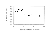
表1に第1粉末のD50の測定結果を示す。また、図1にBサイト原料粉末(TiO2粉末)のBET値と第1粉末のD50の関係を示している。表1及び図1より、BET値を20m2/g以上にすることにより、第1粉末のD50を1.0μm以下、さらには0.8μm以下にできることがわかる。このことは、同一の粉砕時間でより微細な誘電体粉末を得ることができることを示しており、本発明によれば、粉砕による歪が少なく誘電特性の高い微細な誘電体粉末が得られることを示唆している。 Table 1 shows the measurement results of D50 of the first powder. FIG. 1 shows the relationship between the BET value of the B-site raw material powder (TiO 2 powder) and D50 of the first powder. From Table 1 and FIG. 1, it can be seen that by setting the BET value to 20 m 2 / g or more, the D50 of the first powder can be 1.0 μm or less, and further 0.8 μm or less. This indicates that a finer dielectric powder can be obtained with the same pulverization time. According to the present invention, it is possible to obtain a fine dielectric powder with less dielectric distortion and high dielectric properties. Suggests.
次に、9種類の第1粉末100モルに対して以下の副成分の粉末を添加した後に、ボールミルにより湿式混合した。ボールミルとして、4寸ポット及びメディアとしてZrO2ボール(φ10mm:200g、φ3mm:430g)を用い、120rpmで16時間処理した。また、ポットには第1粉末を100g投入し、スラリー濃度を33%とした。さらに、混合に先立ち、分散剤(東亞合成(株)製:A−30SL)を0.2wt%添加した。
MnO(D50=0.55μm):0.365モル
V2O5(D50=0.52μm):0.1モル
Y2O3(D50=0.33μm):0.035モル
CaSiO3(D50=1.178μm):1.616モル
Next, after adding the powder of the following subcomponents with respect to 100 mols of nine kinds of first powders, wet mixing was performed by a ball mill. Using a 4-inch pot as a ball mill and ZrO 2 balls (φ10 mm: 200 g, φ3 mm: 430 g) as media, treatment was performed at 120 rpm for 16 hours. In addition, 100 g of the first powder was introduced into the pot, and the slurry concentration was 33%. Further, prior to mixing, 0.2 wt% of a dispersant (manufactured by Toagosei Co., Ltd .: A-30SL) was added.
MnO (D50 = 0.55 μm): 0.365 mol V 2 O 5 (D50 = 0.52 μm): 0.1 mol Y 2 O 3 (D50 = 0.33 μm): 0.035 mol CaSiO 3 (D50 = 1.178 μm): 1.616 mol
ボールミルによる湿式混合が終了した後に、乾燥機を用いて120℃の温度下で24時間保持して乾燥した。
乾燥された混合粉末を355μmのメッシュを通した後、MgO製のコウバチ中において、1150℃で2時間保持することにより焼成(第2焼成)を行った。
After the wet mixing by the ball mill was completed, it was dried using a drier at a temperature of 120 ° C. for 24 hours.
The dried mixed powder was passed through a 355 μm mesh, and then fired (second firing) by being held at 1150 ° C. for 2 hours in a MgO bee.
ボールミルを用いて得られた焼成物(第2焼成物)を粉砕した。ボールミルとして、4寸ポット及びメディアとしてZrO2ボール(φ10mm:200g、φ3mm:430g)を用い、120rpmで16時間処理した。また、ボールミルには焼成物を100g投入し、スラリー濃度を33%とした。
ボールミルによる湿式混合が終了した後に、乾燥機を用いて120℃の温度下で24時間保持して乾燥した。この粉末を、以下第2粉末と言うことにする。
The fired product (second fired product) obtained using a ball mill was pulverized. Using a 4-inch pot as a ball mill and ZrO 2 balls (φ10 mm: 200 g, φ3 mm: 430 g) as media, treatment was performed at 120 rpm for 16 hours. The ball mill was charged with 100 g of the fired product and the slurry concentration was 33%.
After the wet mixing by the ball mill was completed, it was dried using a drier at a temperature of 120 ° C. for 24 hours. This powder is hereinafter referred to as a second powder.
以上で得られた第2粉末と有機高分子樹脂とをポットミルを用いて混練した。有機高分子樹脂としては、ベンジル系樹脂(εr =2.5、tanδ=1×10⁻⁴)を用いた。混練は、100mlのポット中にφ10mmのZrO2ボールを60g投入し、120rpmで3時間処理した。また、ポット中に、第2粉末を15g、ベンジル系樹脂を第2粉末の含有率が40vol%になるように投入した。
混練終了後、混練物をシート状に成形した後に、乾燥機にて110℃で2時間保持する乾燥を行った。その後、150℃の温度でプレス成形後、180℃に昇温して樹脂を完全に硬化させた。樹脂の硬化後に、シートから1mm角、長さ80mm以上の寸法の試料(複合誘電体材料)を切出した。
The second powder obtained above and the organic polymer resin were kneaded using a pot mill. As the organic polymer resin, a benzyl resin (εr = 2.5, tan δ = 1 × 10 −4 ) was used. For kneading, 60 g of φ10 mm ZrO 2 balls were put into a 100 ml pot and treated at 120 rpm for 3 hours. Also, 15 g of the second powder and benzyl resin were added into the pot so that the content of the second powder was 40 vol%.
After completion of the kneading, the kneaded product was formed into a sheet and then dried by holding at 110 ° C. for 2 hours in a dryer. Then, after press molding at a temperature of 150 ° C., the temperature was raised to 180 ° C. to completely cure the resin. After the resin was cured, a sample (composite dielectric material) having a size of 1 mm square and a length of 80 mm or more was cut out from the sheet.
以上の複合誘電体材料について比誘電率(εr)とQ値を摂動法(n=3)により測定した。その結果を表1に示す。なお、測定にはヒューレットパッカード社製のRFベクトルネットワークアナライザであるHP8510を用いて行った。
図2にBサイト原料粉末のBET値と、複合誘電体材料の比誘電率(εr)及びQ値との関係を示す。図2に示すように、Bサイト原料粉末のBET値が大きくなるにつれて複合誘電体材料の比誘電率(εr)及びQ値が大きくなる。しかし、BET値が30m2/gをピークに、複合誘電体材料の比誘電率(εr)及びQ値が低下する傾向にある。この結果より、本発明では、複合誘電体材料を得る場合、Bサイト原料粉末のBET値を20〜40m2/g、望ましくは25〜35m2/gの範囲とする。
The dielectric constant (εr) and Q value of the above composite dielectric material were measured by the perturbation method (n = 3). The results are shown in Table 1. The measurement was performed using an HP 8510, an RF vector network analyzer manufactured by Hewlett-Packard Company.
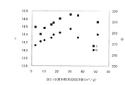
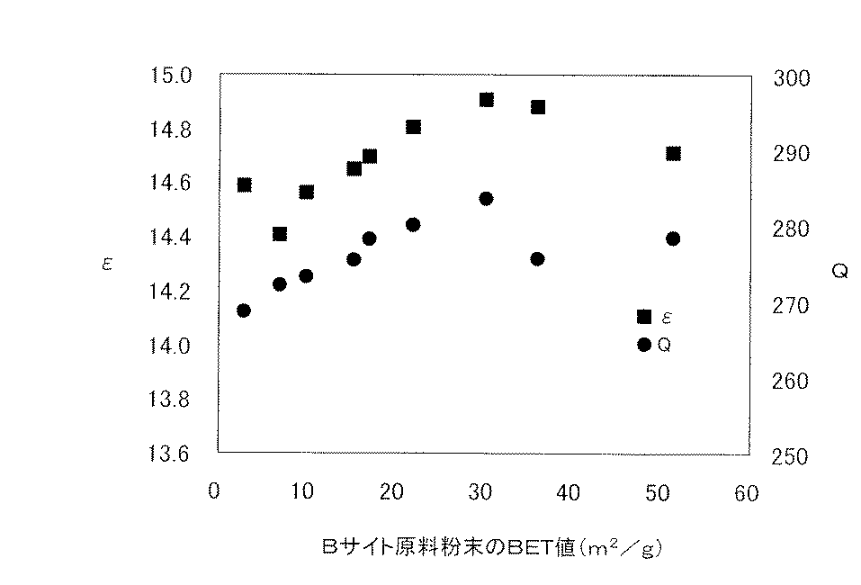
FIG. 2 shows the relationship between the BET value of the B site raw material powder, the relative dielectric constant (εr) and the Q value of the composite dielectric material. As shown in FIG. 2, as the BET value of the B-site raw material powder increases, the relative dielectric constant (εr) and Q value of the composite dielectric material increase. However, the relative dielectric constant (εr) and the Q value of the composite dielectric material tend to decrease with the BET value peaking at 30 m 2 / g. From this result, in the present invention, when obtaining a composite dielectric material, the B-site raw material powder has a BET value of 20 to 40 m 2 / g, preferably 25 to 35 m 2 / g.
Claims (7)
Aサイトを構成するAサイト原料粉末とBサイトを構成するBET値が20m2/g以上のBサイト原料粉末とを含む混合物を焼成して第1焼成物を得る第1焼成工程と、
前記第1焼成物を粉砕して第1粉末を得る第1粉砕工程と、を備えることを特徴とする誘電体粉末の製造方法。 A method for producing a dielectric powder containing a perovskite oxide having an ABO 3 type atomic arrangement,
A first firing step of firing a mixture containing the A site raw material powder constituting the A site and the B site raw material powder having a BET value of 20 m 2 / g or more constituting the B site to obtain a first fired product;
And a first pulverization step of pulverizing the first fired product to obtain a first powder.
前記第2焼成物を粉砕して第2粉末を得る第2粉砕工程と、を備えることを特徴とする請求項1に記載の誘電体粉末の製造方法。 A second firing step of obtaining a second fired product by firing after applying a predetermined treatment to the first powder obtained in the first grinding step;
The method for producing a dielectric powder according to claim 1, further comprising: a second pulverization step of pulverizing the second fired product to obtain a second powder.
Aサイトを構成するAサイト原料粉末とBサイトを構成するBET値が20〜40m2/gのBサイト原料粉末とを原料とする焼成物を粉砕して誘電体粉末を得る工程と、
前記誘電体粉末と樹脂を複合化する工程と、を備えることを特徴とする複合誘電体材料の製造方法。 A method for producing a composite dielectric material comprising a dielectric powder comprising a perovskite oxide having an ABO 3 type atomic arrangement and a resin,
A step of obtaining a dielectric powder by pulverizing a fired product made from an A site raw material powder constituting the A site and a B site raw material powder having a BET value of 20 to 40 m 2 / g constituting the B site;
And a step of compositing the dielectric powder and a resin.
Priority Applications (1)
| Application Number | Priority Date | Filing Date | Title |
|---|---|---|---|
| JP2004036612A JP2005225721A (en) | 2004-02-13 | 2004-02-13 | Production method for dielectric powder and production method for composite dielectric material |
Applications Claiming Priority (1)
| Application Number | Priority Date | Filing Date | Title |
|---|---|---|---|
| JP2004036612A JP2005225721A (en) | 2004-02-13 | 2004-02-13 | Production method for dielectric powder and production method for composite dielectric material |
Publications (1)
| Publication Number | Publication Date |
|---|---|
| JP2005225721A true JP2005225721A (en) | 2005-08-25 |
Family
ID=35000728
Family Applications (1)
| Application Number | Title | Priority Date | Filing Date |
|---|---|---|---|
| JP2004036612A Withdrawn JP2005225721A (en) | 2004-02-13 | 2004-02-13 | Production method for dielectric powder and production method for composite dielectric material |
Country Status (1)
| Country | Link |
|---|---|
| JP (1) | JP2005225721A (en) |
Cited By (4)
| Publication number | Priority date | Publication date | Assignee | Title |
|---|---|---|---|---|
| JP2007126661A (en) * | 2005-11-02 | 2007-05-24 | Samsung Electro Mech Co Ltd | Dielectric polymer ceramic composition and built-in capacitor and print circuit substrate board using the same |
| JP2007290944A (en) * | 2006-03-27 | 2007-11-08 | Kyocera Corp | Barium calcium titanate powder and production method thereof |
| WO2008087986A1 (en) * | 2007-01-18 | 2008-07-24 | Nippon Chemical Industrial Co., Ltd. | Inorganic filler and composite dielectric material using the same |
| WO2013115045A1 (en) * | 2012-01-30 | 2013-08-08 | モメンティブ・パフォーマンス・マテリアルズ・ジャパン合同会社 | Resin composition with high dielectric insulation properties |
-
2004
- 2004-02-13 JP JP2004036612A patent/JP2005225721A/en not_active Withdrawn
Cited By (11)
| Publication number | Priority date | Publication date | Assignee | Title |
|---|---|---|---|---|
| JP2007126661A (en) * | 2005-11-02 | 2007-05-24 | Samsung Electro Mech Co Ltd | Dielectric polymer ceramic composition and built-in capacitor and print circuit substrate board using the same |
| JP2007290944A (en) * | 2006-03-27 | 2007-11-08 | Kyocera Corp | Barium calcium titanate powder and production method thereof |
| WO2008087986A1 (en) * | 2007-01-18 | 2008-07-24 | Nippon Chemical Industrial Co., Ltd. | Inorganic filler and composite dielectric material using the same |
| JPWO2008087986A1 (en) * | 2007-01-18 | 2010-05-06 | 日本化学工業株式会社 | Inorganic filler and composite dielectric material using the same |
| WO2013115045A1 (en) * | 2012-01-30 | 2013-08-08 | モメンティブ・パフォーマンス・マテリアルズ・ジャパン合同会社 | Resin composition with high dielectric insulation properties |
| JP2013177558A (en) * | 2012-01-30 | 2013-09-09 | Momentive Performance Materials Inc | Resin composition with high dielectric insulation property |
| CN103717679A (en) * | 2012-01-30 | 2014-04-09 | 迈图高新材料日本合同公司 | Resin composition with high dielectric insulation properties |
| KR20140117255A (en) * | 2012-01-30 | 2014-10-07 | 모멘티브 파포만스 마테리아루즈 쟈판 고도가이샤 | Resin composition with high dielectric insulation properties |
| US9343196B2 (en) | 2012-01-30 | 2016-05-17 | Momentive Performance Materials Japan Llc | Resin composition with high dielectric insulation properties |
| CN103717679B (en) * | 2012-01-30 | 2017-05-10 | 迈图高新材料日本合同公司 | Resin composition with high dielectric insulation properties |
| KR101967695B1 (en) | 2012-01-30 | 2019-04-11 | 모멘티브 파포만스 마테리아루즈 쟈판 고도가이샤 | Resin composition with high dielectric insulation properties |
Similar Documents
| Publication | Publication Date | Title |
|---|---|---|
| KR100687178B1 (en) | Manufacturing method of spherical oxide powder and apparatus for producing spherical powder | |
| CN103864406B (en) | A kind of dielectric constant microwave ceramic medium and preparation method thereof | |
| KR100627112B1 (en) | Dielectric Ceramics Powder, Method of Preparing Dielectric Ceramics Powder and Complex Dielectric Material | |
| CN1319909C (en) | Microwave dielectric composition and method for producing same | |
| JP3930814B2 (en) | Composite dielectric material and substrate | |
| KR100642148B1 (en) | Method for producing dielectric ceramic powder | |
| JP2005225721A (en) | Production method for dielectric powder and production method for composite dielectric material | |
| JP2005225735A (en) | Production method for dielectric porcelain composition | |
| JP2005302435A (en) | Composite dielectric material | |
| WO1996008019A1 (en) | Dielectric procelain composition and its manufacture | |
| KR20120045712A (en) | Co2z type ferrite for rf application, method of preparing the same and antenna employing the same | |
| CN115246736A (en) | Nickel Zinc Copper Ferrites for VUHF Antenna Applications | |
| JP4465663B2 (en) | Dielectric porcelain composition | |
| JP2005259357A (en) | Dielectric powder, composite dielectric material, manufacturing method of dielectric powder and manufacturing method of composite dielectric material | |
| JP2007048703A (en) | Composite dielectric material and prepreg using this, metal foil coated object, molding body, composite dielectric substrate, and multilayer substrate | |
| JP2004168579A (en) | Dielectric porcelain composition and dielectric resonator | |
| JP2006344407A (en) | Composite dielectric material, prepreg using the same, metal foil painted object, molded compact, composite dielectric base board, multi-layered base board, and manufacturing method of composite dielectric material | |
| JP2007045690A (en) | Dielectric porcelain composition | |
| JP2008088004A (en) | Method of manufacturing dielectric porcelain composition | |
| JP6064732B2 (en) | Magnetic oxide sintered body and high-frequency magnetic component using the same | |
| JP2006265062A (en) | Dielectric ceramic composition | |
| JP2005225719A (en) | Dielectric ceramic composition | |
| Bisht et al. | Microwave dielectrics: solid solution, ordering and microwave dielectric properties of $$(1 {-} x)\hbox {Ba}(\hbox {Mg} _ {1/3}\hbox {Nb} _ {2/3})\hbox {O} _ {3}{-} x\hbox {Ba (Mg} _ {1/8}\hbox {Nb} _ {3/4})\hbox {O} _ {3} $$ ceramics. | |
| JP2006256931A (en) | Dielectric porcelain composition | |
| JP2006265078A (en) | Dielectric ceramic composition and composite dielectric material using it |
Legal Events
| Date | Code | Title | Description |
|---|---|---|---|
| A621 | Written request for application examination |
Free format text: JAPANESE INTERMEDIATE CODE: A621 Effective date: 20061204 |
|
| A761 | Written withdrawal of application |
Free format text: JAPANESE INTERMEDIATE CODE: A761 Effective date: 20090217 |