JP2006270060A - 受光素子と受光素子を用いた光通信用受信モジュールおよび受光素子を用いた計測器 - Google Patents
受光素子と受光素子を用いた光通信用受信モジュールおよび受光素子を用いた計測器 Download PDFInfo
- Publication number
- JP2006270060A JP2006270060A JP2006035880A JP2006035880A JP2006270060A JP 2006270060 A JP2006270060 A JP 2006270060A JP 2006035880 A JP2006035880 A JP 2006035880A JP 2006035880 A JP2006035880 A JP 2006035880A JP 2006270060 A JP2006270060 A JP 2006270060A
- Authority
- JP
- Japan
- Prior art keywords
- light receiving
- inp
- layer
- light
- receiving element
- Prior art date
- Legal status (The legal status is an assumption and is not a legal conclusion. Google has not performed a legal analysis and makes no representation as to the accuracy of the status listed.)
- Granted
Links
Images




Landscapes
- Light Receiving Elements (AREA)
Abstract
【課題】 InP基板の上に結晶性の良い欠陥の少ない受光層を形成することによって1.65μm〜3.0μmの中赤外光を受光できる製造容易で暗電流の小さい受光素子を与えること。
【解決手段】 InP基板の上に直接にあるいはInPバッファ層を介して1.65μm〜3.0μmの範囲にバンドギャップを持つGaInNAsP受光層又はGaInNAsSb受光層或いはGaInNAsPSb受光層を設け、InP窓層或いはInAlAs窓層をその上に設けるかあるいは設けず、マスクして亜鉛を選択拡散してp領域を形成しp電極をつける。GaInNAsP、GaInNAsSb或いはGaInNAsPSbはInP基板と格子整合(不整合度±0.2%以下)するので格子定数を徐々に変化させるグレーディッド層が不要である。InP基板はn−InPでもSI−InPでもよい。
1.65μm〜3.0μmの中赤外光の受光素子を製造することができる。
【選択図】 図2
Description
本発明のInP基板はn−InP基板とは限らない。半絶縁性基板SI−InPを用いることもできる。
具体的な組成はGa0.47In0.53N0.018As0.982(従来例)とGa0.47In0.53N0.018As0.932Sb0.05(本発明)である。これは従来例のAs原子の一部をSbによって置き換えたものである。原子間力顕微鏡(AFM)によって両方のサンプルの表面の凹凸を観察した。
図18はGa0.47In0.53N0.018As0.982(従来例)の表面を示す。顕微鏡写真によっても表面の荒さがよく分る。一本の直線にそった面の凹凸をグラフで示した。横軸は線分に沿った寸法であり5μmの長さを示す。縦軸は表面の微小な凹凸でありフルスケールは±25nmである。10nm〜5nm程度の凹凸が多数見られる。±15nmもの凹凸がある。表面の荒れが甚だしく面粗度は大きい。
図19はGa0.47In0.53N0.018As0.932Sb0.05(本発明)の表面をしめす。顕微鏡写真によっても表面の平坦度の優れていることがよく分る。一本の直線にそった面の凹凸をグラフで示した。横軸は線分に沿った寸法であり0.7μmの長さを示す。縦軸は表面の微小な凹凸でありフルスケールは±2.5nmである。図18のスケールの1/10であることに注意すべきである。0.3nm〜0.1nm程度の凹凸はあるが極めて滑らかで平坦であることが分る。面粗度は図18の従来例のものの大体1/30以下になっている。図19の試料はSbを5at%添加しただけで他の条件は同じである。だから表面状態が改善されたのはSb添加の効果である。
電極・層構造は上から順に、
p電極8/SiN膜7
ノンドープInP窓層5(d=1.5μm)/Zn拡散領域6
n−GaInNAsP4(Siドープ;n=3×1015cm−3、d=1μm)
ノンドープInPバッファ層3(d=2μm)
n−InP基板2(Sドープ)
n電極10
というようになっている。
図2に示すような構造の受光素子を製作した。電極・層構造は上から順に、
ノンドープInP窓層5(d=1.5μm)/Zn拡散領域6
n−GaInNAsSb24(Siドープ;n=3×1015cm−3、d=1μm)
ノンドープInPバッファ層3(d=1μm)
n−InP基板2(Sドープ)
n電極10
というようになっている。
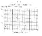
(100)ジャストでフォトルミネッセンス(PL)が0.1、オフ角が2度でフォトルミネッセンスが0.25である。オフ角が5度でフォトルミネッセンスは1.0に上がる。オフ角が10度で最大値1.2を取る。オフ角が13度でPLは1.0である。オフ角が15度でPLは0.9に低下する。オフ角が20度でPLは1.15となる。20度を越えるとPLは低下し始める。オフ角が25度でPLは0.3に落ちる。オフ角が33度でPLは0.05に低下する。
この測定からSb濃度が1at%の場合、望ましいInP基板のオフアングルは5度〜20度であることがわかる。この結果はGaInNAsSb受光層のものであるが、GaInNAsP受光層でも同様な結果が得られた。
(100)ジャストでフォトルミネッセンス(PL)が0.1である。これはSb=1at%の場合と同じである。オフ角が0.2度でフォトルミネセンスが0.9に強くなる。オフ角が2度でフォトルミネッセンスは1.3に上がる。オフ角が5度でフォトルミネッセンスは1.0になる。オフ角が10度でフォトルミネセンスは0.9を取る。オフ角が13度でPLは1.0である。オフ角が15度でPLは0.9に低下する。オフ角が20度でPLは0.85に落ちる。20度を越えるとPLは低下し始める。オフ角が25度でPLは0.25に落ちる。オフ角が33度でPLは0.05に低下する。
この測定からSb濃度が5at%の場合、望ましいInP基板のオフアングルは0.2度〜20度であることがわかる。この結果はGaInNAsSb受光層(Sb=5at%)のものであるが、Sb濃度が20at%以下であれば同様の結果が得られた。GaInNAsP受光層(P濃度0.01at%〜10at%)でもPの濃度を2at%に増やすことによって同様な結果が得られた。
さらにGaInNAsPSb(Pの濃度0.01at%〜10at%、Sbの濃度0.1at%〜20at%)の場合でも同様の結果が得られた。
[Sb濃度およびP濃度の上限について]
Sbの濃度が20at%を越えるとフォトルミネセンスがほとんど得られなくなる。またノンドープでのキャリヤ濃度が1×1017cm−3を越えるというように結晶純度が低下して、受光素子には使えないレベルの結晶純度しか得られなかった。
Pの濃度についても10at%を越えるとエピ表面に曇りが生じ、フォトルミネセンスが殆ど得られなくなり、受光素子に用いることができない。
実施例2で作製したGaInNAsSb/InP受光素子を用いて光通信用受信モジュールを作製した。受光径200μmである。暗電流は3nA@5Vを得た。さらに感度の波長依存性を調べた。その結果を図10に示す。横軸は波長(Wavelength:nm)である。縦軸は相対感度(Relative Sensitivity:dB)である。光通信で使われる通常のInGaAs/InP受光素子の感度の波長依存性も調べた。
実施例2で作製したGaInNAsSb/InP受光素子を用いて土壌の水分量を測定した。図6に示すように水は1450nmと1950nmに吸収のピークを持つ。2900nm〜3100nmも吸収が大きい。土壌水分はこれまで静電容量の変化などで測定する技術があったが、光学的に測定する技術は未だない。優れたセンサがないからである。水分を測定するためには上のような水に特有の吸収スペクトルピークの光をあて吸収光を計測すればよい。
実施例2で作製したGaInNAsSb/InP受光素子を用いてプラスチックの分別システムを作製した。ポリエチレンテレフタレート(PET)の吸収スペクトルは図7のようである。横軸は波長(nm)縦軸はスペクトル強度である。
さまざまのプラスチックからPETを選別する必要がある。一つの波長の光を測定していたのではPETと他の材料の区別がつかない。幾つかの選ばれた波長を使ってその波長の光の吸収あるいは透過を幾つかのフォトダイオードで測定する。それを、ニューラルネットワークを応用してスペクトル強度比を認識してPETを他の物質から選別できた。
実施例2で作製したGaInNAsSb/InP受光素子を用いてりんごの糖度を測定した。1〜2μmまでに見られるりんごの糖分による吸収から推定した糖度と従来の破壊検査法で測定した糖度の相関を調べた結果、糖度(10〜20%)において、±1%の精度で測定できる結果を得た。
(1)図16に示すような構造の受光素子を製作した。
電極・層構造は上から順に、
p電極8/SiN膜7
In0.53Ga0.47Asキャップ層26(n=5×1015cm−3、d=0.02μm)
SiドープIn0.52Al0.48As窓層25(n=5×1015cm−3、d=0.6μm)/Zn拡散領域6
n−Ga0.47In0.53N0.018As0.9315P0.0005Sb0.05層14(ノンドープ;n=8×1015cm−3、d=2μm)
ノンドープInPバッファ層13(d=1μm)
n−InP基板2(Sドープ)
n電極10
というようになっている。この受光層はPが0.05at%、Sbが5at%のGaInNAsPSbである。
受光径200μmφのpin型PDを作製した。逆バイアス電圧1Vでの暗電流は1nAであり十分小さい。良好なPDであった。
3 InPバッファ層
4 GaInNAsP受光層(光吸収層)
5 n−InP窓層
6 Zn拡散領域
7 保護膜 (SiN、SiO2)
8 p電極
9 pn接合
10 n電極
13 ノンドープInP層
14 GaInNAsPSb受光層(光吸収層)
24 GaInNAsSb受光層 (光吸収層)
25 InAlAs窓層
26 InGaAsキャップ層
30 SI−InP基板
32 n−InP
33 n−InP
34 GaInNAsP
35 InP
36 Zn拡散領域
37 保護膜
38 p電極
39 pn接合
40 n電極
Claims (16)
- InP基板と、その上に設けられバンドギャップ波長が1.65μm〜3.0μmであるGaInNAsP受光層(光吸収層)とを有する事を特徴とする受光素子。
- GaInNAsP受光層におけるPの濃度は0.01at%〜10at%であることを特徴とする請求項1に記載の受光素子。
- InP基板の格子定数をaとし、GaInNAsPとInPの格子定数の差をΔaとして、GaInNAsPはInP基板に対して|Δa/a|≦0.2%となるような格子整合度を有することを特徴とする請求項1に記載の受光素子。
- InP基板と、その上に設けられバンドギャップ波長が1.65μm〜3.0μmであるGaInNAsSb受光層(光吸収層)とを有する事を特徴とする受光素子。
- GaInNAsSb受光層においてSbの濃度が0.1at%〜20at%である事を特徴とする請求項4に記載の受光素子。
- InP基板の格子定数をaとし、GaInNAsSbとInPの格子定数の差をΔaとして、GaInNAsSbはInP基板に対して|Δa/a|≦0.2%となるような格子整合度を有することを特徴とする請求項4に記載の受光素子。
- InP基板と、その上に設けられバンドギャップ波長が1.65μm〜3.0μmであるGaInNAsPSb受光層(光吸収層)とを有することを特徴とする受光素子
- GaInNAsPSb受光層においてPの濃度は0.01at%〜10at%、Sbの濃度は0.1at%〜20at%であることを特徴とする請求項7に記載の受光素子。
- InP基板の格子定数をaとし、GaInNAsPSbの格子定数とInPの格子定数の差をΔaとして、GaInNAsPSbはInP基板に対して|Δa/a|≦0.2%となるような格子定数を有することを特徴とする請求項7に記載の受光素子。
- InP基板は(100)から[111]方向または[11−1]方向に0.2度〜20度傾斜したオフアングル基板であることを特徴とする請求項1〜9の何れかに記載の受光素子。
- InP基板はFeドープした半絶縁性であることを特徴とする請求項1〜10の何れかに記載の受光素子。
- 受光層の上にInP窓層あるいはInAlAs窓層を備えることを特徴とする請求項1〜11の何れかに記載の受光素子。
- 請求項1から12の何れかに記載の受光素子を含む事を特徴とする光通信用受光モジュール。
- 請求項1から12の何れかに記載の受光素子を用いた事を特徴とする水分濃度計測器。
- 請求項1から12の何れかに記載の受光素子を用いた事を特徴とする糖度計測器。
- 請求項1から12の何れかに記載の受光素子を用いた事を特徴とするプラスチック選別用計測器。
Priority Applications (1)
| Application Number | Priority Date | Filing Date | Title |
|---|---|---|---|
| JP2006035880A JP5008874B2 (ja) | 2005-02-23 | 2006-02-14 | 受光素子と受光素子を用いた光通信用受信モジュールおよび受光素子を用いた計測器 |
Applications Claiming Priority (3)
| Application Number | Priority Date | Filing Date | Title |
|---|---|---|---|
| JP2005046465 | 2005-02-23 | ||
| JP2005046465 | 2005-02-23 | ||
| JP2006035880A JP5008874B2 (ja) | 2005-02-23 | 2006-02-14 | 受光素子と受光素子を用いた光通信用受信モジュールおよび受光素子を用いた計測器 |
Publications (2)
| Publication Number | Publication Date |
|---|---|
| JP2006270060A true JP2006270060A (ja) | 2006-10-05 |
| JP5008874B2 JP5008874B2 (ja) | 2012-08-22 |
Family
ID=37205622
Family Applications (1)
| Application Number | Title | Priority Date | Filing Date |
|---|---|---|---|
| JP2006035880A Expired - Fee Related JP5008874B2 (ja) | 2005-02-23 | 2006-02-14 | 受光素子と受光素子を用いた光通信用受信モジュールおよび受光素子を用いた計測器 |
Country Status (1)
| Country | Link |
|---|---|
| JP (1) | JP5008874B2 (ja) |
Cited By (25)
| Publication number | Priority date | Publication date | Assignee | Title |
|---|---|---|---|---|
| WO2008084772A1 (ja) * | 2007-01-10 | 2008-07-17 | Sumitomo Electric Industries, Ltd. | 受光素子 |
| JP2008270760A (ja) * | 2007-03-23 | 2008-11-06 | Sumitomo Electric Ind Ltd | 半導体ウエハ、その製造方法および半導体素子 |
| WO2009014076A1 (ja) * | 2007-07-23 | 2009-01-29 | Sumitomo Electric Industries, Ltd. | 受光デバイス |
| WO2010073770A1 (ja) * | 2008-12-25 | 2010-07-01 | 住友電気工業株式会社 | 気体モニタリング装置、燃焼状態モニタリング装置、経年変化モニタリング装置、および不純物濃度モニタリング装置 |
| WO2011027624A1 (ja) * | 2009-09-07 | 2011-03-10 | 住友電気工業株式会社 | Iii-v族化合物半導体受光素子、iii-v族化合物半導体受光素子を作製する方法、受光素子、及び、エピタキシャルウェハ |
| JP2011060853A (ja) * | 2009-09-07 | 2011-03-24 | Sumitomo Electric Ind Ltd | Iii−v族化合物半導体受光素子、及びiii−v族化合物半導体受光素子を作製する方法 |
| JP2011060855A (ja) * | 2009-09-07 | 2011-03-24 | Sumitomo Electric Ind Ltd | 受光素子及びエピタキシャルウェハ |
| JP2011100770A (ja) * | 2009-11-04 | 2011-05-19 | Sumitomo Electric Ind Ltd | 受光素子アレイの製造方法及び受光素子アレイ、並びにエピタキシャルウェハの製造方法及びエピタキシャルウェハ |
| JP2011109146A (ja) * | 2011-03-01 | 2011-06-02 | Sumitomo Electric Ind Ltd | Iii−v族化合物半導体受光素子 |
| US7999231B2 (en) | 2008-08-29 | 2011-08-16 | Sumitomo Electric Inductries, Ltd. | Moisture detector, biological body moisture detector, natural product moisture detector, and product/material moisture detector |
| US8188559B2 (en) | 2008-02-01 | 2012-05-29 | Sumitomo Electric Industries, Ltd. | Light-receiving element and light-receiving element array |
| US8243139B2 (en) | 2008-09-11 | 2012-08-14 | Sumitomo Electric Industries, Ltd. | Image pickup device, visibility support apparatus, night vision device, navigation support apparatus, and monitoring device |
| US8373156B2 (en) | 2008-12-22 | 2013-02-12 | Sumitomo Electric Industries, Ltd. | Biological component detection device |
| WO2013065639A1 (ja) * | 2011-11-01 | 2013-05-10 | 住友電気工業株式会社 | 受光素子、エピタキシャルウエハおよびその製造方法 |
| US8546758B2 (en) | 2008-09-22 | 2013-10-01 | Sumitomo Electric Industries, Ltd. | Food quality examination device, food component examination device, foreign matter component examination device, taste examination device, and changed state examination device |
| JP2014064009A (ja) * | 2013-10-15 | 2014-04-10 | Sumitomo Electric Ind Ltd | 受光素子及びエピタキシャルウェハ |
| JP2015043466A (ja) * | 2014-12-01 | 2015-03-05 | 住友電気工業株式会社 | Iii−v族化合物半導体受光素子 |
| JP2017181705A (ja) * | 2016-03-30 | 2017-10-05 | 富士フイルム株式会社 | 組成物、膜、光学フィルタ、積層体、固体撮像素子、画像表示装置および赤外線センサ |
| US9985152B2 (en) | 2010-03-29 | 2018-05-29 | Solar Junction Corporation | Lattice matchable alloy for solar cells |
| US10355159B2 (en) | 2010-10-28 | 2019-07-16 | Solar Junction Corporation | Multi-junction solar cell with dilute nitride sub-cell having graded doping |
| US10916675B2 (en) | 2015-10-19 | 2021-02-09 | Array Photonics, Inc. | High efficiency multijunction photovoltaic cells |
| US10930808B2 (en) | 2017-07-06 | 2021-02-23 | Array Photonics, Inc. | Hybrid MOCVD/MBE epitaxial growth of high-efficiency lattice-matched multijunction solar cells |
| US11211514B2 (en) | 2019-03-11 | 2021-12-28 | Array Photonics, Inc. | Short wavelength infrared optoelectronic devices having graded or stepped dilute nitride active regions |
| US11233166B2 (en) | 2014-02-05 | 2022-01-25 | Array Photonics, Inc. | Monolithic multijunction power converter |
| US11271122B2 (en) | 2017-09-27 | 2022-03-08 | Array Photonics, Inc. | Short wavelength infrared optoelectronic devices having a dilute nitride layer |
Citations (5)
| Publication number | Priority date | Publication date | Assignee | Title |
|---|---|---|---|---|
| JPH05218591A (ja) * | 1992-01-31 | 1993-08-27 | Furukawa Electric Co Ltd:The | 半導体レーザ素子および半導体受光素子 |
| JPH10126005A (ja) * | 1996-08-28 | 1998-05-15 | Ricoh Co Ltd | 半導体発光素子及び半導体発光素子の製造方法 |
| JP2000332229A (ja) * | 1999-05-18 | 2000-11-30 | Canon Inc | Si基板上の光電融合デバイス構造及びその製造方法 |
| JP2003051644A (ja) * | 2001-08-02 | 2003-02-21 | Furukawa Electric Co Ltd:The | 半導体装置、半導体受光装置、半導体発光装置、半導体レーザ装置および面発光型半導体レーザ装置 |
| WO2005078512A1 (ja) * | 2004-02-17 | 2005-08-25 | The Furukawa Electric Co., Ltd. | フォトニック結晶半導体デバイスおよびその製造方法 |
-
2006
- 2006-02-14 JP JP2006035880A patent/JP5008874B2/ja not_active Expired - Fee Related
Patent Citations (5)
| Publication number | Priority date | Publication date | Assignee | Title |
|---|---|---|---|---|
| JPH05218591A (ja) * | 1992-01-31 | 1993-08-27 | Furukawa Electric Co Ltd:The | 半導体レーザ素子および半導体受光素子 |
| JPH10126005A (ja) * | 1996-08-28 | 1998-05-15 | Ricoh Co Ltd | 半導体発光素子及び半導体発光素子の製造方法 |
| JP2000332229A (ja) * | 1999-05-18 | 2000-11-30 | Canon Inc | Si基板上の光電融合デバイス構造及びその製造方法 |
| JP2003051644A (ja) * | 2001-08-02 | 2003-02-21 | Furukawa Electric Co Ltd:The | 半導体装置、半導体受光装置、半導体発光装置、半導体レーザ装置および面発光型半導体レーザ装置 |
| WO2005078512A1 (ja) * | 2004-02-17 | 2005-08-25 | The Furukawa Electric Co., Ltd. | フォトニック結晶半導体デバイスおよびその製造方法 |
Cited By (36)
| Publication number | Priority date | Publication date | Assignee | Title |
|---|---|---|---|---|
| WO2008084772A1 (ja) * | 2007-01-10 | 2008-07-17 | Sumitomo Electric Industries, Ltd. | 受光素子 |
| JP2008171912A (ja) * | 2007-01-10 | 2008-07-24 | Sumitomo Electric Ind Ltd | 受光素子 |
| US8120061B2 (en) | 2007-01-10 | 2012-02-21 | Sumitomo Electric Industries, Ltd. | Light receiving device |
| JP2008270760A (ja) * | 2007-03-23 | 2008-11-06 | Sumitomo Electric Ind Ltd | 半導体ウエハ、その製造方法および半導体素子 |
| WO2009014076A1 (ja) * | 2007-07-23 | 2009-01-29 | Sumitomo Electric Industries, Ltd. | 受光デバイス |
| JP2009027049A (ja) * | 2007-07-23 | 2009-02-05 | Sumitomo Electric Ind Ltd | 受光デバイス |
| US8058642B2 (en) | 2007-07-23 | 2011-11-15 | Sumitomo Electric Industries, Ltd. | Light-receiving device |
| US8729527B2 (en) | 2008-02-01 | 2014-05-20 | Sumitomo Electric Industries, Ltd. | Light-receiving element, light-receiving element array, method for manufacturing light-receiving element and method for manufacturing light-receiving element array |
| US8188559B2 (en) | 2008-02-01 | 2012-05-29 | Sumitomo Electric Industries, Ltd. | Light-receiving element and light-receiving element array |
| US7999231B2 (en) | 2008-08-29 | 2011-08-16 | Sumitomo Electric Inductries, Ltd. | Moisture detector, biological body moisture detector, natural product moisture detector, and product/material moisture detector |
| US8564666B2 (en) | 2008-09-11 | 2013-10-22 | Sumitomo Electric Industries, Ltd. | Image pickup device, visibility support apparatus, night vision device, navigation support apparatus, and monitoring device |
| EP2328187A4 (en) * | 2008-09-11 | 2014-08-06 | Sumitomo Electric Industries | PICTURE RECEIVER, VISIBILITY SUPPORT DEVICE, NIGHT VISOR, NAVIGATION SUPPORT DEVICE AND MONITORING DEVICE |
| US8243139B2 (en) | 2008-09-11 | 2012-08-14 | Sumitomo Electric Industries, Ltd. | Image pickup device, visibility support apparatus, night vision device, navigation support apparatus, and monitoring device |
| US8546758B2 (en) | 2008-09-22 | 2013-10-01 | Sumitomo Electric Industries, Ltd. | Food quality examination device, food component examination device, foreign matter component examination device, taste examination device, and changed state examination device |
| US8373156B2 (en) | 2008-12-22 | 2013-02-12 | Sumitomo Electric Industries, Ltd. | Biological component detection device |
| WO2010073770A1 (ja) * | 2008-12-25 | 2010-07-01 | 住友電気工業株式会社 | 気体モニタリング装置、燃焼状態モニタリング装置、経年変化モニタリング装置、および不純物濃度モニタリング装置 |
| US8624189B2 (en) | 2008-12-25 | 2014-01-07 | Sumitomo Electric Industries, Ltd. | Gas monitoring device, combustion state monitoring device, secular change monitoring device, and impurity concentration monitoring device |
| US9159853B2 (en) | 2009-09-07 | 2015-10-13 | Sumitomo Electric Industries, Ltd. | Group III-V compound semiconductor photo detector, method of fabricating group III-V compound semiconductor photo detector, photo detector, and epitaxial wafer |
| US8866199B2 (en) | 2009-09-07 | 2014-10-21 | Sumitomo Electric Industries, Ltd. | Group III-V compound semiconductor photo detector, method of fabricating group III-V compound semiconductor photo detector, photo detector, and epitaxial wafer |
| JP2011060855A (ja) * | 2009-09-07 | 2011-03-24 | Sumitomo Electric Ind Ltd | 受光素子及びエピタキシャルウェハ |
| JP2011060853A (ja) * | 2009-09-07 | 2011-03-24 | Sumitomo Electric Ind Ltd | Iii−v族化合物半導体受光素子、及びiii−v族化合物半導体受光素子を作製する方法 |
| WO2011027624A1 (ja) * | 2009-09-07 | 2011-03-10 | 住友電気工業株式会社 | Iii-v族化合物半導体受光素子、iii-v族化合物半導体受光素子を作製する方法、受光素子、及び、エピタキシャルウェハ |
| JP2011100770A (ja) * | 2009-11-04 | 2011-05-19 | Sumitomo Electric Ind Ltd | 受光素子アレイの製造方法及び受光素子アレイ、並びにエピタキシャルウェハの製造方法及びエピタキシャルウェハ |
| US9985152B2 (en) | 2010-03-29 | 2018-05-29 | Solar Junction Corporation | Lattice matchable alloy for solar cells |
| US10355159B2 (en) | 2010-10-28 | 2019-07-16 | Solar Junction Corporation | Multi-junction solar cell with dilute nitride sub-cell having graded doping |
| JP2011109146A (ja) * | 2011-03-01 | 2011-06-02 | Sumitomo Electric Ind Ltd | Iii−v族化合物半導体受光素子 |
| JP2013098385A (ja) * | 2011-11-01 | 2013-05-20 | Sumitomo Electric Ind Ltd | 受光素子、エピタキシャルウエハおよびその製造方法 |
| WO2013065639A1 (ja) * | 2011-11-01 | 2013-05-10 | 住友電気工業株式会社 | 受光素子、エピタキシャルウエハおよびその製造方法 |
| JP2014064009A (ja) * | 2013-10-15 | 2014-04-10 | Sumitomo Electric Ind Ltd | 受光素子及びエピタキシャルウェハ |
| US11233166B2 (en) | 2014-02-05 | 2022-01-25 | Array Photonics, Inc. | Monolithic multijunction power converter |
| JP2015043466A (ja) * | 2014-12-01 | 2015-03-05 | 住友電気工業株式会社 | Iii−v族化合物半導体受光素子 |
| US10916675B2 (en) | 2015-10-19 | 2021-02-09 | Array Photonics, Inc. | High efficiency multijunction photovoltaic cells |
| JP2017181705A (ja) * | 2016-03-30 | 2017-10-05 | 富士フイルム株式会社 | 組成物、膜、光学フィルタ、積層体、固体撮像素子、画像表示装置および赤外線センサ |
| US10930808B2 (en) | 2017-07-06 | 2021-02-23 | Array Photonics, Inc. | Hybrid MOCVD/MBE epitaxial growth of high-efficiency lattice-matched multijunction solar cells |
| US11271122B2 (en) | 2017-09-27 | 2022-03-08 | Array Photonics, Inc. | Short wavelength infrared optoelectronic devices having a dilute nitride layer |
| US11211514B2 (en) | 2019-03-11 | 2021-12-28 | Array Photonics, Inc. | Short wavelength infrared optoelectronic devices having graded or stepped dilute nitride active regions |
Also Published As
| Publication number | Publication date |
|---|---|
| JP5008874B2 (ja) | 2012-08-22 |
Similar Documents
| Publication | Publication Date | Title |
|---|---|---|
| JP5008874B2 (ja) | 受光素子と受光素子を用いた光通信用受信モジュールおよび受光素子を用いた計測器 | |
| US9391229B2 (en) | Light receiving element, semiconductor epitaxial wafer, detecting device, and method for manufacturing light receiving element | |
| US7875906B2 (en) | Photodetector and production method thereof | |
| Campbell et al. | Quantum-dot infrared photodetectors | |
| US9312422B2 (en) | Light receiving element, semiconductor epitaxial wafer, method for manufacturing the light receiving element, method for manufacturing the semiconductor epitaxial wafer, and detecting device | |
| JP5975417B2 (ja) | 受光素子の製造方法 | |
| Boras et al. | III–V ternary nanowires on Si substrates: growth, characterization and device applications | |
| Park et al. | Monolithic two-color short-wavelength InGaAs infrared photodetectors using InAsP metamorphic buffers | |
| US7915639B2 (en) | InGaAsSbN photodiode arrays | |
| US9608148B2 (en) | Semiconductor element and method for producing the same | |
| JP2008288293A (ja) | 半導体受光素子 | |
| US20130043459A1 (en) | Long Wavelength Infrared Superlattice | |
| JP2012009777A (ja) | 半導体ウエハおよび半導体装置 | |
| Ren et al. | Epitaxially grown III-arsenide-antimonide nanowires for optoelectronic applications | |
| US9276159B2 (en) | Superlattice structure | |
| US8426845B2 (en) | Long wavelength infrared superlattice | |
| US20130043458A1 (en) | Long Wavelength Infrared Superlattice | |
| JP2009027046A (ja) | 受光素子 | |
| JP2010225820A (ja) | 半導体受光素子 | |
| Ahmad | A Study of GaAs1-xSbx Axial Nanowires and PIN Junctions by Self Catalyzed Molecular Beam Epitaxy | |
| Fraser et al. | Status of multi-wafer production MBE capabilities for extended SWIR III-V epi materials for IR detection | |
| Tan et al. | GaInNAsSb/GaAs Photodiodes for Long-Wavelength Applications | |
| Hsieh et al. | Strain relaxation properties of InAs y P 1− y metamorphic buffer layers for SWIR InGaAs photodetector | |
| Yu et al. | Bias-tunable broadband light-emitting/detecting devices based on the III-V nanowires on Si-substrate | |
| Bin et al. | Metamorphic InGaAs pin photodetectors with 1.75 μm cut-off wavelength grown on GaAs |
Legal Events
| Date | Code | Title | Description |
|---|---|---|---|
| A621 | Written request for application examination |
Free format text: JAPANESE INTERMEDIATE CODE: A621 Effective date: 20090206 |
|
| A977 | Report on retrieval |
Free format text: JAPANESE INTERMEDIATE CODE: A971007 Effective date: 20101007 |
|
| TRDD | Decision of grant or rejection written | ||
| A01 | Written decision to grant a patent or to grant a registration (utility model) |
Free format text: JAPANESE INTERMEDIATE CODE: A01 Effective date: 20120509 |
|
| A01 | Written decision to grant a patent or to grant a registration (utility model) |
Free format text: JAPANESE INTERMEDIATE CODE: A01 |
|
| A61 | First payment of annual fees (during grant procedure) |
Free format text: JAPANESE INTERMEDIATE CODE: A61 Effective date: 20120530 |
|
| R150 | Certificate of patent or registration of utility model |
Ref document number: 5008874 Country of ref document: JP Free format text: JAPANESE INTERMEDIATE CODE: R150 Free format text: JAPANESE INTERMEDIATE CODE: R150 |
|
| FPAY | Renewal fee payment (event date is renewal date of database) |
Free format text: PAYMENT UNTIL: 20150608 Year of fee payment: 3 |
|
| R250 | Receipt of annual fees |
Free format text: JAPANESE INTERMEDIATE CODE: R250 |
|
| S111 | Request for change of ownership or part of ownership |
Free format text: JAPANESE INTERMEDIATE CODE: R313117 |
|
| R350 | Written notification of registration of transfer |
Free format text: JAPANESE INTERMEDIATE CODE: R350 |
|
| R250 | Receipt of annual fees |
Free format text: JAPANESE INTERMEDIATE CODE: R250 |
|
| R250 | Receipt of annual fees |
Free format text: JAPANESE INTERMEDIATE CODE: R250 |
|
| R250 | Receipt of annual fees |
Free format text: JAPANESE INTERMEDIATE CODE: R250 |
|
| R250 | Receipt of annual fees |
Free format text: JAPANESE INTERMEDIATE CODE: R250 |
|
| LAPS | Cancellation because of no payment of annual fees |