JP2006287226A - はんだ結合を形成するために規定された層列を有する半導体チップ及び支持体と半導体チップとの間にはんだ結合を形成するための方法 - Google Patents
はんだ結合を形成するために規定された層列を有する半導体チップ及び支持体と半導体チップとの間にはんだ結合を形成するための方法 Download PDFInfo
- Publication number
- JP2006287226A JP2006287226A JP2006094778A JP2006094778A JP2006287226A JP 2006287226 A JP2006287226 A JP 2006287226A JP 2006094778 A JP2006094778 A JP 2006094778A JP 2006094778 A JP2006094778 A JP 2006094778A JP 2006287226 A JP2006287226 A JP 2006287226A
- Authority
- JP
- Japan
- Prior art keywords
- layer
- semiconductor chip
- solder
- barrier layer
- oxidation protection
- Prior art date
- Legal status (The legal status is an assumption and is not a legal conclusion. Google has not performed a legal analysis and makes no representation as to the accuracy of the status listed.)
- Pending
Links
Images
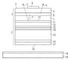

Classifications
-
- H—ELECTRICITY
- H10—SEMICONDUCTOR DEVICES; ELECTRIC SOLID-STATE DEVICES NOT OTHERWISE PROVIDED FOR
- H10W—GENERIC PACKAGES, INTERCONNECTIONS, CONNECTORS OR OTHER CONSTRUCTIONAL DETAILS OF DEVICES COVERED BY CLASS H10
- H10W72/00—Interconnections or connectors in packages
- H10W72/30—Die-attach connectors
-
- H—ELECTRICITY
- H10—SEMICONDUCTOR DEVICES; ELECTRIC SOLID-STATE DEVICES NOT OTHERWISE PROVIDED FOR
- H10H—INORGANIC LIGHT-EMITTING SEMICONDUCTOR DEVICES HAVING POTENTIAL BARRIERS
- H10H20/00—Individual inorganic light-emitting semiconductor devices having potential barriers, e.g. light-emitting diodes [LED]
- H10H20/80—Constructional details
- H10H20/85—Packages
- H10H20/857—Interconnections, e.g. lead-frames, bond wires or solder balls
-
- H—ELECTRICITY
- H10—SEMICONDUCTOR DEVICES; ELECTRIC SOLID-STATE DEVICES NOT OTHERWISE PROVIDED FOR
- H10W—GENERIC PACKAGES, INTERCONNECTIONS, CONNECTORS OR OTHER CONSTRUCTIONAL DETAILS OF DEVICES COVERED BY CLASS H10
- H10W72/00—Interconnections or connectors in packages
- H10W72/071—Connecting or disconnecting
- H10W72/073—Connecting or disconnecting of die-attach connectors
-
- H—ELECTRICITY
- H10—SEMICONDUCTOR DEVICES; ELECTRIC SOLID-STATE DEVICES NOT OTHERWISE PROVIDED FOR
- H10W—GENERIC PACKAGES, INTERCONNECTIONS, CONNECTORS OR OTHER CONSTRUCTIONAL DETAILS OF DEVICES COVERED BY CLASS H10
- H10W72/00—Interconnections or connectors in packages
- H10W72/071—Connecting or disconnecting
- H10W72/073—Connecting or disconnecting of die-attach connectors
- H10W72/07331—Connecting techniques
- H10W72/07336—Soldering or alloying
-
- H—ELECTRICITY
- H10—SEMICONDUCTOR DEVICES; ELECTRIC SOLID-STATE DEVICES NOT OTHERWISE PROVIDED FOR
- H10W—GENERIC PACKAGES, INTERCONNECTIONS, CONNECTORS OR OTHER CONSTRUCTIONAL DETAILS OF DEVICES COVERED BY CLASS H10
- H10W72/00—Interconnections or connectors in packages
- H10W72/30—Die-attach connectors
- H10W72/351—Materials of die-attach connectors
- H10W72/352—Materials of die-attach connectors comprising metals or metalloids, e.g. solders
Landscapes
- Die Bonding (AREA)
- Led Device Packages (AREA)
- Led Devices (AREA)
Applications Claiming Priority (2)
| Application Number | Priority Date | Filing Date | Title |
|---|---|---|---|
| DE102005015147 | 2005-03-31 | ||
| DE102005029246.1A DE102005029246B4 (de) | 2005-03-31 | 2005-06-23 | Halbleiterchip mit einer Lötschichtenfolge und Verfahren zum Löten eines Halbleiterchips |
Publications (1)
| Publication Number | Publication Date |
|---|---|
| JP2006287226A true JP2006287226A (ja) | 2006-10-19 |
Family
ID=36869981
Family Applications (1)
| Application Number | Title | Priority Date | Filing Date |
|---|---|---|---|
| JP2006094778A Pending JP2006287226A (ja) | 2005-03-31 | 2006-03-30 | はんだ結合を形成するために規定された層列を有する半導体チップ及び支持体と半導体チップとの間にはんだ結合を形成するための方法 |
Country Status (4)
| Country | Link |
|---|---|
| US (1) | US7598529B2 (fr) |
| EP (1) | EP1717854B1 (fr) |
| JP (1) | JP2006287226A (fr) |
| DE (1) | DE102005029246B4 (fr) |
Cited By (5)
| Publication number | Priority date | Publication date | Assignee | Title |
|---|---|---|---|---|
| JP2015095607A (ja) * | 2013-11-14 | 2015-05-18 | 日亜化学工業株式会社 | 発光装置の製造方法 |
| JP2016515763A (ja) * | 2013-03-26 | 2016-05-30 | オスラム オプト セミコンダクターズ ゲゼルシャフト ミット ベシュレンクテル ハフツングOsram Opto Semiconductors GmbH | In−bi−ag接合層を形成するための等温凝固反応を用いた接合パートナーの接合方法及び対応する複数の接合パートナーの配置構成 |
| KR20180015651A (ko) * | 2015-06-02 | 2018-02-13 | 로저스 저매니 게엠베하 | 복합 재료를 제조하기 위한 방법 |
| WO2018105327A1 (fr) * | 2016-12-07 | 2018-06-14 | 日機装株式会社 | Procédé de production de dispositif à semiconducteur optique |
| JP2020523800A (ja) * | 2017-06-12 | 2020-08-06 | オスラム オーエルイーディー ゲゼルシャフト ミット ベシュレンクテル ハフツングOSRAM OLED GmbH | 半導体チップを基板の上に固定する方法および電子構成素子 |
Families Citing this family (17)
| Publication number | Priority date | Publication date | Assignee | Title |
|---|---|---|---|---|
| DE102005029246B4 (de) | 2005-03-31 | 2023-06-22 | OSRAM Opto Semiconductors Gesellschaft mit beschränkter Haftung | Halbleiterchip mit einer Lötschichtenfolge und Verfahren zum Löten eines Halbleiterchips |
| DE102007029391A1 (de) * | 2007-06-26 | 2009-01-02 | Osram Opto Semiconductors Gmbh | Optoelektronischer Halbleiterchip |
| US8293587B2 (en) * | 2007-10-11 | 2012-10-23 | International Business Machines Corporation | Multilayer pillar for reduced stress interconnect and method of making same |
| DE102008026839A1 (de) | 2007-12-20 | 2009-07-02 | Osram Opto Semiconductors Gmbh | Verfahren zum Herstellen eines optoelektronischen Bauelements in Dünnschichttechnik |
| DE102008050573A1 (de) | 2008-10-06 | 2010-04-08 | Osram Opto Semiconductors Gmbh | Verfahren zur Herstellung eines optoelektronischen Halbleiterbauelements und optoelektronisches Halbleiterbauelement |
| US20100101639A1 (en) * | 2008-10-24 | 2010-04-29 | Epistar Corporation | Optoelectronic device having a multi-layer solder and manufacturing method thereof |
| KR100974776B1 (ko) * | 2009-02-10 | 2010-08-06 | 엘지이노텍 주식회사 | 발광 소자 |
| TWI401825B (zh) | 2009-11-27 | 2013-07-11 | 財團法人工業技術研究院 | 發光二極體晶片的固晶方法及固晶完成之發光二極體 |
| CN102104090B (zh) * | 2009-12-22 | 2014-03-19 | 财团法人工业技术研究院 | 发光二极管芯片固晶方法、固晶的发光二极管及芯片结构 |
| TWI446577B (zh) * | 2010-12-23 | 2014-07-21 | 財團法人工業技術研究院 | Led晶圓之接合方法、led晶粒之製造方法及led晶圓與基體之接合結構 |
| US9490193B2 (en) | 2011-12-01 | 2016-11-08 | Infineon Technologies Ag | Electronic device with multi-layer contact |
| DE102012216546B4 (de) * | 2012-09-17 | 2023-01-19 | Infineon Technologies Ag | Verfahren zum verlöten eines halbleiterchips mit einem träger |
| DE102013206260B3 (de) * | 2013-04-10 | 2014-09-11 | Schott Ag | Verfahren zum Herstellen eines Bauelements mit einer Lötverbindung, Bauelement mit Lötverbindung und Verwendung des Bauelements |
| DE102013109316A1 (de) | 2013-05-29 | 2014-12-04 | Osram Opto Semiconductors Gmbh | Verfahren zur Herstellung einer Mehrzahl von optoelektronischen Halbleiterchips und optoelektronischer Halbleiterchip |
| DE102015108545A1 (de) | 2015-05-29 | 2016-12-01 | Osram Opto Semiconductors Gmbh | Optoelektronisches Bauelement und Verfahren zur Herstellung eines optoelektronischen Bauelements |
| CN111699430B (zh) | 2018-01-29 | 2022-07-22 | 应用材料公司 | 用于光学器件增强的润湿层 |
| CN113601063A (zh) * | 2021-08-16 | 2021-11-05 | 苏州三利特新能源科技有限公司 | 一种基于纳米改性的高润湿无铅光伏焊带及其制备方法 |
Citations (4)
| Publication number | Priority date | Publication date | Assignee | Title |
|---|---|---|---|---|
| JPH10190130A (ja) * | 1996-12-27 | 1998-07-21 | Shimadzu Corp | 半導体レーザ装置 |
| JP2001057468A (ja) * | 1999-08-18 | 2001-02-27 | Hitachi Ltd | はんだ接続構造を有する回路装置およびその製造方法 |
| JP2004141937A (ja) * | 2002-10-25 | 2004-05-20 | Mitsubishi Materials Corp | はんだペースト用表面被覆Au−Sn合金粉末 |
| JP2004260178A (ja) * | 2003-02-26 | 2004-09-16 | Osram Opto Semiconductors Gmbh | 光電子半導体チップに用いられる電気的なコンタクトならびに該電気的なコンタクトを製造するための方法 |
Family Cites Families (14)
| Publication number | Priority date | Publication date | Assignee | Title |
|---|---|---|---|---|
| DE1614668B2 (de) | 1967-12-01 | 1974-08-29 | Semikron Gesellschaft Fuer Gleichrichterbau Und Elektronik Mbh, 8500 Nuernberg | Halbleiter-Anordnung mit Großflächigen, gut lötbaren Kontaktelektroden und Verfahren zu ihrer Herstellung |
| US4817854A (en) * | 1985-03-11 | 1989-04-04 | The United States Of America As Represented By The Secretary Of The Air Force | LED soldering method utilizing a PT migration barrier |
| US5197654A (en) | 1991-11-15 | 1993-03-30 | Avishay Katz | Bonding method using solder composed of multiple alternating gold and tin layers |
| US5234153A (en) * | 1992-08-28 | 1993-08-10 | At&T Bell Laboratories | Permanent metallic bonding method |
| JPH1064902A (ja) * | 1996-07-12 | 1998-03-06 | Applied Materials Inc | アルミニウム材料の成膜方法及び成膜装置 |
| US5990560A (en) | 1997-10-22 | 1999-11-23 | Lucent Technologies Inc. | Method and compositions for achieving a kinetically controlled solder bond |
| EP1179836A3 (fr) | 2000-08-11 | 2003-05-28 | Agere Systems Optoelectronics Guardian Corporation | Contact pour dispositifs semiconducteurs d'indium comprenant des soudures d'or |
| US6661098B2 (en) * | 2002-01-18 | 2003-12-09 | International Business Machines Corporation | High density area array solder microjoining interconnect structure and fabrication method |
| DE10221857A1 (de) * | 2002-05-16 | 2003-11-27 | Osram Opto Semiconductors Gmbh | Verfahren zum Befestigen eines Halbleiterchips in einem Kunststoffgehäusekörper, optoelektronisches Halbleiterbauelement und Verfahren zu dessen Herstellung |
| US6929966B2 (en) * | 2002-11-29 | 2005-08-16 | Osram Opto Semiconductors Gmbh | Method for producing a light-emitting semiconductor component |
| JP2004235649A (ja) * | 2003-01-31 | 2004-08-19 | Osram Opto Semiconductors Gmbh | 電気コンタクト領域を備えたモジュールの製造方法および半導体層列および活性ゾーンを有するモジュール |
| DE10350707B4 (de) | 2003-02-26 | 2014-02-13 | Osram Opto Semiconductors Gmbh | Elektrischer Kontakt für optoelektronischen Halbleiterchip und Verfahren zu dessen Herstellung |
| DE10329364B4 (de) * | 2003-06-30 | 2007-10-11 | Osram Opto Semiconductors Gmbh | Elektrischer Kontakt für ein optoelekronisches Bauelement und Verfahren zu dessen Herstellung |
| DE102005029246B4 (de) | 2005-03-31 | 2023-06-22 | OSRAM Opto Semiconductors Gesellschaft mit beschränkter Haftung | Halbleiterchip mit einer Lötschichtenfolge und Verfahren zum Löten eines Halbleiterchips |
-
2005
- 2005-06-23 DE DE102005029246.1A patent/DE102005029246B4/de not_active Expired - Lifetime
-
2006
- 2006-03-03 EP EP06004421.1A patent/EP1717854B1/fr not_active Expired - Lifetime
- 2006-03-30 US US11/393,533 patent/US7598529B2/en active Active
- 2006-03-30 JP JP2006094778A patent/JP2006287226A/ja active Pending
Patent Citations (4)
| Publication number | Priority date | Publication date | Assignee | Title |
|---|---|---|---|---|
| JPH10190130A (ja) * | 1996-12-27 | 1998-07-21 | Shimadzu Corp | 半導体レーザ装置 |
| JP2001057468A (ja) * | 1999-08-18 | 2001-02-27 | Hitachi Ltd | はんだ接続構造を有する回路装置およびその製造方法 |
| JP2004141937A (ja) * | 2002-10-25 | 2004-05-20 | Mitsubishi Materials Corp | はんだペースト用表面被覆Au−Sn合金粉末 |
| JP2004260178A (ja) * | 2003-02-26 | 2004-09-16 | Osram Opto Semiconductors Gmbh | 光電子半導体チップに用いられる電気的なコンタクトならびに該電気的なコンタクトを製造するための方法 |
Cited By (14)
| Publication number | Priority date | Publication date | Assignee | Title |
|---|---|---|---|---|
| JP2016515763A (ja) * | 2013-03-26 | 2016-05-30 | オスラム オプト セミコンダクターズ ゲゼルシャフト ミット ベシュレンクテル ハフツングOsram Opto Semiconductors GmbH | In−bi−ag接合層を形成するための等温凝固反応を用いた接合パートナーの接合方法及び対応する複数の接合パートナーの配置構成 |
| JP2015095607A (ja) * | 2013-11-14 | 2015-05-18 | 日亜化学工業株式会社 | 発光装置の製造方法 |
| JP2018524250A (ja) * | 2015-06-02 | 2018-08-30 | ロジャーズ ジャーマニー ゲーエムベーハーRogers Germany GmbH | 複合材料を製作するための方法 |
| KR20180015651A (ko) * | 2015-06-02 | 2018-02-13 | 로저스 저매니 게엠베하 | 복합 재료를 제조하기 위한 방법 |
| KR102571961B1 (ko) | 2015-06-02 | 2023-08-28 | 로저스 저매니 게엠베하 | 복합 재료를 제조하기 위한 방법 |
| US10439100B2 (en) | 2016-12-07 | 2019-10-08 | Nikkiso Co., Ltd. | Method of manufacturing optical semiconductor apparatus |
| JP2018093137A (ja) * | 2016-12-07 | 2018-06-14 | 日機装株式会社 | 光半導体装置の製造方法 |
| WO2018105327A1 (fr) * | 2016-12-07 | 2018-06-14 | 日機装株式会社 | Procédé de production de dispositif à semiconducteur optique |
| JP2020523800A (ja) * | 2017-06-12 | 2020-08-06 | オスラム オーエルイーディー ゲゼルシャフト ミット ベシュレンクテル ハフツングOSRAM OLED GmbH | 半導体チップを基板の上に固定する方法および電子構成素子 |
| JP7003239B2 (ja) | 2017-06-12 | 2022-01-20 | オスラム オーエルイーディー ゲゼルシャフト ミット ベシュレンクテル ハフツング | 半導体チップを基板の上に固定する方法および電子構成素子 |
| JP2022050511A (ja) * | 2017-06-12 | 2022-03-30 | オスラム オーエルイーディー ゲゼルシャフト ミット ベシュレンクテル ハフツング | 半導体チップを基板の上に固定する方法および電子構成素子 |
| US11315898B2 (en) | 2017-06-12 | 2022-04-26 | Osram Oled Gmbh | Method for fastening a semiconductor chip on a substrate, and electronic component |
| JP7248774B2 (ja) | 2017-06-12 | 2023-03-29 | オスラム オーエルイーディー ゲゼルシャフト ミット ベシュレンクテル ハフツング | 半導体チップを基板の上に固定する方法および電子構成素子 |
| JP2023072078A (ja) * | 2017-06-12 | 2023-05-23 | オスラム オーエルイーディー ゲゼルシャフト ミット ベシュレンクテル ハフツング | 半導体チップを基板の上に固定する方法および電子構成素子 |
Also Published As
| Publication number | Publication date |
|---|---|
| US20060234482A1 (en) | 2006-10-19 |
| DE102005029246A1 (de) | 2006-10-12 |
| US7598529B2 (en) | 2009-10-06 |
| EP1717854A3 (fr) | 2011-05-11 |
| EP1717854A2 (fr) | 2006-11-02 |
| EP1717854B1 (fr) | 2020-07-29 |
| DE102005029246B4 (de) | 2023-06-22 |
Similar Documents
| Publication | Publication Date | Title |
|---|---|---|
| TWI389336B (zh) | And a method of manufacturing the light-emitting element and the light-emitting element | |
| US7247514B2 (en) | Semiconductor device and method for producing the same | |
| US7219825B2 (en) | SnAgAu solder bumps, method of manufacturing the same, and method of bonding light emitting device using the same | |
| US7598529B2 (en) | Semiconductor chip having a soldering layer sequence, and process for soldering a semiconductor chip | |
| US7666692B2 (en) | Semiconductor device, its manufacture method and electronic component unit | |
| JP5111693B2 (ja) | 反射特性を有する接触部を備えた発光構造及びその製造方法 | |
| JP3982284B2 (ja) | サブマウントおよび半導体装置 | |
| US7612384B2 (en) | Reflective electrode for a semiconductor light emitting apparatus | |
| JP5426081B2 (ja) | 基板接合方法及び半導体装置 | |
| CN110770894B (zh) | 用于将半导体芯片固定在基板上的方法和电子器件 | |
| JPH0750813B2 (ja) | 半導体レーザ素子用サブマウント | |
| JP2004327982A (ja) | 半導体装置およびその製造方法 | |
| JP2012069545A (ja) | 発光素子の搭載方法 | |
| JP2001230498A (ja) | Iii族窒化物系化合物半導体レーザ | |
| CN116368615A (zh) | 发光器件、发光模组及其制备方法 | |
| JP4537877B2 (ja) | セラミックス配線基板とそれを用いた半導体装置 | |
| JP2009004716A (ja) | Led装置の製造方法 | |
| JP2007251142A (ja) | 半田層及びそれを用いた電子デバイス接合用基板並びにその製造方法 | |
| US20130193580A1 (en) | Method of manufacturing semiconductor device and semiconductor device | |
| JPS59165474A (ja) | 半導体発光素子 | |
| KR101578485B1 (ko) | 반도체 발광소자 | |
| JP2004014795A (ja) | 窒化物半導体レーザ用サブマウントおよびこれを用いた窒化物半導体レーザ | |
| JP2006286943A (ja) | サブマウント基板及びその製造方法 |
Legal Events
| Date | Code | Title | Description |
|---|---|---|---|
| A621 | Written request for application examination |
Free format text: JAPANESE INTERMEDIATE CODE: A621 Effective date: 20090127 |
|
| RD04 | Notification of resignation of power of attorney |
Free format text: JAPANESE INTERMEDIATE CODE: A7424 Effective date: 20101228 |
|
| A977 | Report on retrieval |
Free format text: JAPANESE INTERMEDIATE CODE: A971007 Effective date: 20111220 |
|
| A131 | Notification of reasons for refusal |
Free format text: JAPANESE INTERMEDIATE CODE: A131 Effective date: 20111222 |
|
| A601 | Written request for extension of time |
Free format text: JAPANESE INTERMEDIATE CODE: A601 Effective date: 20120314 |
|
| A602 | Written permission of extension of time |
Free format text: JAPANESE INTERMEDIATE CODE: A602 Effective date: 20120319 |
|
| A521 | Request for written amendment filed |
Free format text: JAPANESE INTERMEDIATE CODE: A523 Effective date: 20120622 |
|
| A02 | Decision of refusal |
Free format text: JAPANESE INTERMEDIATE CODE: A02 Effective date: 20121012 |